Mammoth J201 User manual

Item Quantity Position Part
1 3 C1, C2, C3 .22uF
2 1 C4 .01uF
3 1 C5 47uF
4 2 R1, R4 1M
5 2 R3, R6 6.8K
6 2 R2, R5 2.2K
7 2 R8 3.3K
8 1 D1 1N4001
9 1 D2 (On/Off Indicator) Green LED
10 1 R7 500KA
11 2 Q1, Q2 J201
12 1 Output Jack 1/4” Mono Jack
13 1 Input Jack 1/4” Stereo Jack
14 1 On/Off Switch 3PDT Stomp Switch
15 1 DC Power Jack DC Power Jack
16 1 (optional) Battery Snap
17 1 (On/Off Indicator) LED Bezel
18 1 On/Off Switch 3PDT Wiring Board
19 1 Main PCB J201 PCB
20 1 Standalone Module Click-Less Module
J201 CLEAN BOOST ASSEMBLY INSTRUCTIONS
RECOMMENDED TOOL AND SUPPLY LIST
J201 CLEAN BOOST KIT PARTS LIST
Thank you for purchasing the J201 Clean Boost Pedal Kit from Mammoth Electronics! This is a intermediate level kit that and we
have made every effort to make the assembly as easy as possible.
• Soldering station (with temperature control/regulation)
• Solder & Flux
• De-soldering braid or solder sucker
• Wire strippers
• Wire cutters
• Phillips head screwdriver
• Double-stick foam tape
If you have any questions about building the J201 Clean Boost or need any help with trouble-shooting, please send us an
All kits come standard with the following hardware:
• 1 ¼ inch mono jack
• 1 ¼ inch stereo jack
• 1 DC Power jack
• 1 9V Battery Snap
• 1 3PDT wiring board
• 1 LED Bezel
• 1 3PDT stomp switch (if selected)
• 1 Click-Less True Bypass relay board (if selected)
3
4Site
SW1
12 4567
LRG3PDT
Wire to Ground Lug of Battery Clip
Wire to Main Ground Lug of Output Jack
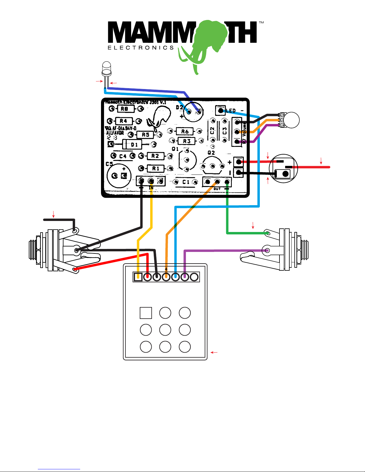
3PDT Wiring Board – Solder Pins to the Lugs of the 3PDT Provided,
Printed-Side of the Board Facing up.
Anode (positive side) of LED.
Connect to Hole 1 of D2 on Main PCB. Cathode (negative side) of LED.
Connect to Hole 2 of D2 on Main PCB
Wiring from the 3PDT Wiring Board (See Diagram)
Pin 1- Input signal to the main board. Wire to connection point labeled “IN”.
Pin 2- Input signal from input jack. Wire to signal lug of input jack.
Pin 3- Main Ground. Wire to center ground lug on input jack
Pin 4- Output signal from main board. Wire to connection point labeled “OUT”.
Pin 5- LED ground (cathode) Wire to connection point labeled “LED –“.
Pin 6- Output signal to the output jack. Wire to signal lug of output jack.
Pin 7- Not used. Can be used as extra ground point if needed. Pins 3 and 7 are tied together.
If you have any questions about building the J201 Clean Boost or need any help with trouble-shooting, please send us an
Positvive Wire of Battery Clip
Wire to Main 9v +
Lug of DC Jack
Wire to DC Jack Ground Lug
500kA

Wiring from the Click-Less PCB (See Diagram)
Pin + : Wire to Main 9V power lug of DC Jack
Pin - : Wire to Main ground lug of input jack
Pin C : Not Used
Pin S2: Wire to lug of N/O SPDT Click-Less switch
Pin S1: Wire to lug of N/O SPDT Click-Less switch
Pin L: Wire to anode (positive leg) of LED
Pin R: Wire to connection point labeled “OUT”
Pin O: Wire to signal lug of output jack
Pin I: Wire to signal lug of input jack
Pin S: Wire to connection point labeled “IN”
If you have any questions about building the J201 Clean Boost or need any help with trouble-shooting, please send us an
Wire to Ground Lug of Battery Clip
Wire to Main Ground Lug of Output Jack
Anode (positive side) of LED.
Connect to Pin L of Click-Less PCB. Cathode (negative side) of LED.
Connect to Hole 2 of D2 on Main PCB
Positvive Wire of Battery Clip
Wire to Main 9v +
Lug of DC Jack
Wire to DC Jack Ground Lug
Wire to DC Jack Ground Lug
500kA
Click-Less Momentary
SPDT Foot Switch

Solder Jumper Wire Here
If you have any questions about building the J201 Clean Boost or need any help with trouble-shooting, please send us an
Wire to Ground Lug of Battery Clip
Wire to Main Ground Lug of Output Jack
Anode (positive side) of LED.
Connect to Hole 1 of D2 on Main PCB. Cathode (negative side) of LED.
Connect to Hole 2 of D2 on Main PCB
Positvive Wire of Battery Clip
Wire to Main 9v +
Lug of DC Jack
Wire to DC Jack Ground Lug
500kA
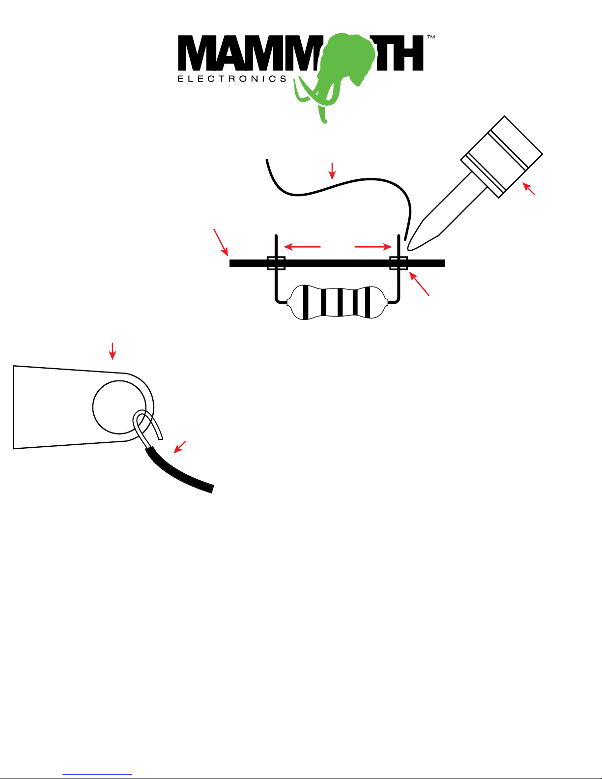
To have Solder that flows
correctly, make sure that
the Soldering Iron is in
contact with the solder pad
and the component’s lead
at the same time. Then
apply your solder until it
flows through to the other
side. After completing your
soldering joint, trim the lead
at the base of the PCB.
solder pad
solder
lug
wire
soldering iron
circuit board / PCB
leads
To attach a wire to a lug of a
jack or pot, strip
approximately 1/4” of the
wire jacket. Wrap the
stripped wire around the
opening in the lug. Clamp
down on the wire so it is
tight on the lug, the apply
solder as you do a part on
the board. The lugs are
much larger than the part
leads and may take more
time to heat before the
solder will flow freely.
If you have any questions about building the J201 Clean Boost or need any help with trouble-shooting, please send us an
COMMON COMPONENTS LEGEND
Q2
D2
D2
R8
D3
C1
This is a Transistor. It has a curved side and
a flat side. Match the flat side of the
transistor with the flat side of the symbol on
the circuit board and install the transistor.
This is an IC (Integrated Circuit). These
have to be installed in a specific fashion.
The two most common indicators are the
square hole of the circuit board symbol
and the notch mark on the circuit board
symbol. The square hole indicates Pin 1 of
the IC. Pin 1 is usually indicated on the IC
by a circle mark in the lower left corner of
the IC, or else the IC will have an indenta-
tion on that side. The leg below the
indentation will be Pin 1. IC sockets will
be matched up by alighning the indenta-
tion marks of the IC and socket.
This is an LED (Light Emitting Diode). It is
Polarized, meaning it has a negative and positive
side. The shorter leg of the LED is typically the
negative side. This can also be indicated on
some LEDs by one side of the edge of the LED
itself being flat. The flat side is the Negative
side. Sometimes the circuit board symbol has a
flat side which indicates the Negative hole.
Otherwise the if not marked with a + or - symbol,
the square hole is the Negative side.
this is a Resistor. It doesn’t have a polarity so it can be installed either
way. The resistor pads will look like this on a circuit board.
This is a diode. Diodes are polarized and must be installed accordingly.
Almost all diodes have a stripe on one side (typically black, silver, or
blue) which indicates the negative side of the diode.Most of the time
the diode symbol on the circuit board will have a stripe as well to
indicate how the diode is to be installed. If the diode does not have a
stripe the the arrow symbol on the circuit board will point to the hole
that the negative lead of the diode goes in.
These are polyfilm, box style, and ceramic capacitors. They are not
polarized so that can be installed either way. On a circuit board their
pads will typically look like this:
This is an Electrolytic Capacitor. Some are polarized, some are not.
General deduction of whether or not it polarized or not is a black or
silver stripe. A non-polarized electrolytic capacitor will not have a stripe.
The negative side of an electrolytic capacitor can also be determined by
the legs of the capacitor. The negaive side will have the shorter leg. The
circuit board symbol indicates the positive or negative side. If it does
not, the square pad in the symbol is the positive hole.
C8


