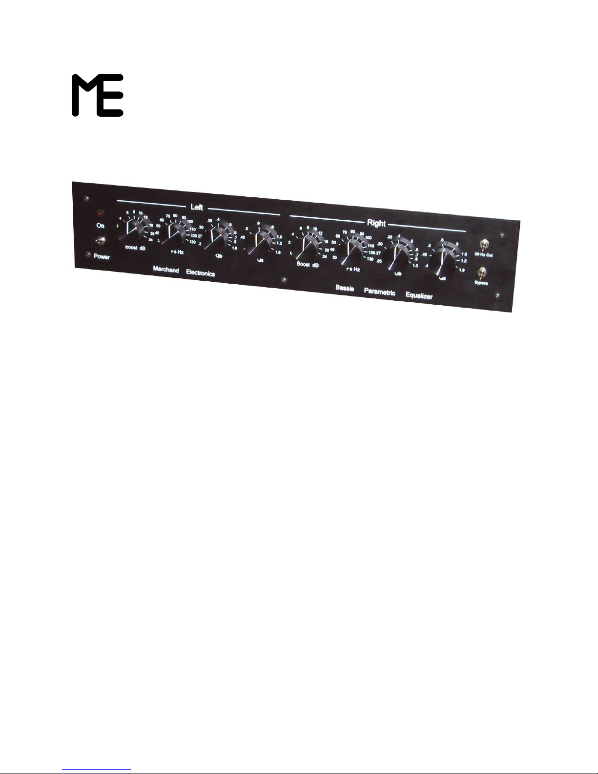
frequencies, pot VR1 is ctu lly l belled BOOST,
with r nge of 0 to 24 dB.
Switch S1 ctiv tes the 20 HZ C T (high-p ss,
infr sonic, or "subsonic") filter with n 18
dB/oct ve slope below 20 Hz, to void the
mplific tion of in udible but potenti lly
destructive low-frequency sign ls. Switch S2
combines the Left nd Right ch nnels t
frequencies below the spe ker's origin l corner
frequency (provided the settings for Fs, Qs,
BOOST, nd Qb re identic l for both ch nnels)
to c ncel out-of-ph se R MBLE sign ls. Switch
S4 provides BYPASS function to elimin te the
equ lizer from the sign l p ther, nd Swith S3
llows the user to reg in t pe monitoring
c p bility, in the event th t the BASSIS is used in
the sole t pe loop of receiver or pre mp.
OPTION 1
If you re constructing your own enclosure for
the BASSIS, you m y choose to c lcul te the
v lues of fixed resistors which reflect your
p rticul r spe ker's Fs nd Qs, nd which provide
fixed mount of boost. This llows you to
elimin te ll but
Single potentiometer -- which controls the
d mping (Qb). Since the setting of the Qb control
influences the level of b ss bout the new corner
frequency (comp re Figures 6 nd 7), you ret in
control of the net b ss extension. To implement
this option, follow the ssembly procedure
det iled in the next section of this m nu l, except:
( ) le ve out the Molex connectors which tt ch
the BOOST nd Fs pots to the PC bo rd; (b) wire
only th t p rt of Molex connector P2 which
tt ches the Qb pot to the PC bo rd; (c)
rec lcul te the v lues of resistors R7, R8, R16,
R4, nd R26 ccording to your spe kers'
ch r cteristics nd the desired mount of boost:
R7 = R8 = 1/(6.28 x Fs x C1)
R16 = R19 x Qs
R4 = R26 = R28 x 10 boost/40.
Where BOOST is given in dB. Now you c n use
du l 10k line r pot to djust the d mping (Qb)
of the Left nd Right ch nnels simult neously.
Or, if you w nt to elimin te the rem ining control
s well, remove VR4 nd rec lcul te R11 for the
desired (fixed) v lue of Qb:
R11 = R2 x Qb.
OPTION 2
There is sp ce in the st nd rd BASSIS
enclosure for n ddition l power supply for
constructors interested in true du l-mono
oper tion. Simply follow the steps in the
"Assembly" section of this m nu l, but wire the
inputs of second + 15 V power supply to the
power cord s well, nd power the Right-ch nnel
PC bo rd from this power supply.
OPTION 3
On the other h nd, if the BASSIS is to be
used with single-ch nnel, independently-
mplified subwoofer, then only single PC bo rd
need be ssembled, nd sm ller enclosure m y
be employed. Assembly is the s me s
described in this m nu l, except th t the switches
m y be SPDT r ther th n DPDT.
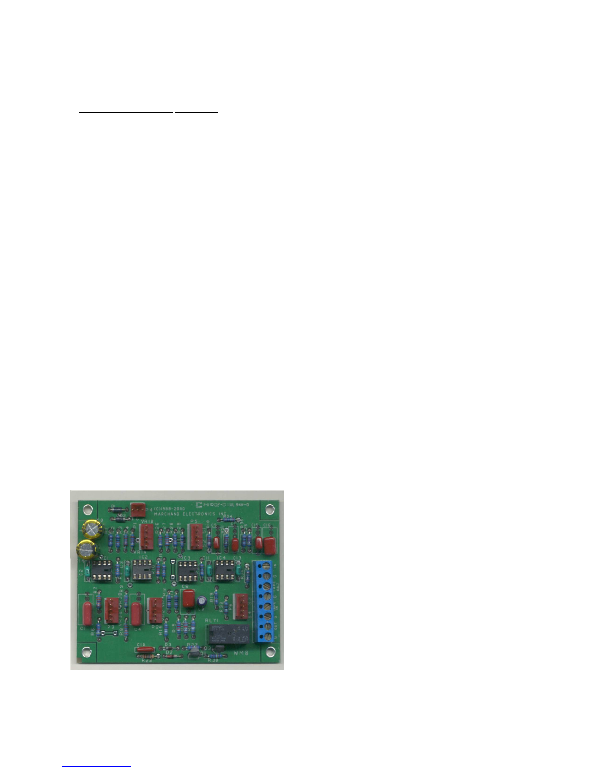
ASSEMBLY (KIT VERSION)
The p rts for stereo implement tion include:
two BASSIS printed circuit bo rds nd
components, one + 15 V power supply ssembly
(such s M rch nd Electronics' Model PS10), nd
one enclosure with h rdw re. The Appendices of
this m nu l cont in det iled Over ll P rts List
s well s PC Bo rd P rts List. You will first
ssemble the circuit bo rds, then mount them in
the enclosure nd tt ch the front p nel controls.
GENERAL WIRING PRACTICE
The tools necess ry to ssemble the BASSIS
include: 15 - 30W soldering pencil, rosin-core
solder, wire cutters, nd Phillips-he d
screwdriver. Other useful tools re:
desoldering tool or solder wick (to remove excess
solder), project holder, long-nose pliers, nd
wire stripper. A cle n, well-lit working re will
minimize frustr tions.
When soldering component to the circuit
bo rd, first mount the component so th t it fits
snugly g inst the silkscreened side of the bo rd.
Next, he t the component le d nd the circuit
bo rd tr ce (on the foil side) simult neously with
the soldering pencil nd pply solder until it melts
nd flows round the component le d. With
pr ctice the entire process should t ke only 5
seconds or so. Remove the pencil nd llow the
connection to cool for few seconds before
moving. Cut off the excess le d close to the
solder joint. If solder bridge w s in dvertently
m de to nother tr ce, remove the solder
c refully with desoldering bulb or br id. Keep
the tip of the soldering pencil cle n by wiping on
d mp sponge every few minutes.
Components c n be identified s follows.
Resistors use the 4-b nd color code in the ch rt
shown below. The fifth b nd is lw ys brown,
indic ting 1% toler nce. For ex mple, resistor
M rch nd Electronics Inc www.m rch ndelec.com
6