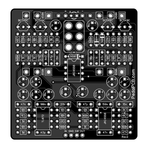
NextGen DB-1 User manual

DB-1 DI-Boost Pedal Kit
(V1.0-2020)
INSTRUCTIONS
This DB-1 DI-Boost Pedal Kit by Next Gen Musical Ltd. is a boost pedal at its core that
can also be ade into a 70's style distortion pedal. It contains instructions for both
configurations, as well as so e advanced distortion odding discussion. It was originally
designed by To Free an of To Free an Audio Effects, a Canadian pedal aker.
BOOST CONFIGURATION
As a boost pedal, the level control is a clean control that can reduce volu e or add a
slight clean boost. The gain control increases the volu e significantly, and introduces a little
grit as it's turned up past 12 o'clock. We suggest running it with the level axed, and the gain
to taste for the a ount of boost you want.
Using an op-a p as the core of the circuit, the pedal can be powered by up to 18V.
The higher the voltage used to power the pedal, the ore clean volu e there is available
before it gets gritty. Note that when built in the "boost" configuration, this is NOT a high gain
pedal. Even with the gain axed out, it adds very little grit to the signal on its own. Boost
pedals are used to overdrive your a p's tubes, or to increase your level a bit for things like
solos.
DISTORTION CONFIGURATION
As a distortion pedal, it's very raw sounding with a lot of attack, si ilar in design to the
classic MXR Distortion+ and Ross Distortions. We have added an advanced odification and
experi entation section that describes how you can experi ent to find the perfect distortion.
Depending on your choice of co ponents, it can be anything fro a subtle distortion to a high
gain onster. See the distortion od section for details, if you're brave enough.
Page 1

TABLE OF CONTENTS
Page 3-4 Kit Contents
Page 4 Reco ended Tools
Page 5-6 PCB Soldering Tips
Page 7 PCB Co ponent Layout
Page 8-15 Pedal Asse bly Instructions
Page 8 - Written Instructions
Page 11 - PCB - Boost Configuration Photo Guide
Page 12 - PCB - Distortion Configuration Photo Guide
Page 13 - Enclosure Asse bly Photo Guide
Page 14 - 3PDT Footswitch Wiring
Page 15 - Finished Product Photo Exa ple
Page 16 Advanced Distortion Modding & Experi entation Discussion
Page 19 Sche atic
Page 20 Basic Troubleshooting
Page 2

KIT CONTENTS
MAIN CONTENTS
PCB's:
1x - Next Gen DIY Kits DB-1 PCB
Resistors:
1x - 100Ω 1/4W Metal Fil Resistor
2x - 1KΩ 1/4W Metal Fil Resistor
2x - 4.7KΩ 1/4W Metal Fil Resistor
3x - 100KΩ 1/4W Metal Fil Resistor
3x - 2.2MΩ 1/4W Metal Fil Resistor
Capacitors:
2x - 0.1uF Polyester Fil Box Capacitor (25V ini u )
4x - 4.7uF Electrolytic Capacitor (radial lead; 25V ini u )
1x - 47uF Electrolytic Capacitor (radial lead; 25V ini u )
1x - 100uF Electrolytic Capacitor (radial lead; 25V ini u )
Diodes:
1x - 1N5817
1x - 5 LED (red)
ICs:
1x - TL072
1x - IC Socket
Potentio eters:
2x - A100K Alpha Mini Solid Shaft Pot (Right Angle PCB)
Jacks & Switches:
1x - Switchcraft #11 Mono Jack
1x - Switchcraft #12B Stereo Jack
1x - Pre iu 3PDT Footswitch
1x - Pre iu External DC Jack (2.1 )
Hardware & Wire:
1x - Ha ond 1590N1 Enclosure
1x - 9V Battery Clip (holder)
1x - 9V Battery Snap
1x - 5 LED Bezel
2x - Knobs for Pots
1x - Bundle of hookup wire (2' black; 2' red, 2' green, and 2' blue)
1x - Set of Adhesive Rubber Feet
Page 3

*ADDITIONS FOR DISTORTION CONFIGURATION*:
1x - Capacitor - 47pF Cera ic Disk Capacitor (25V ini u )
1x - Capacitor - 470pF Cera ic Disk Capacitor (25V ini u )
1x - Capacitor - 4.7nF Polyester Fil Box Capacitor (25V ini u )
1x - Capacitor - 47nF Polyester Fil Box Capacitor (25V ini u )
1x - Capacitor - 1uF Electrolytic Capacitor (25V ini u )
2x - Capacitor - 2.2uF Electrolytic Capacitor (25V ini u )
4x - Diodes - 1N914
1x - Potentio eter - A250K Alpha Mini Solid Shaft Pot (Right Angle PCB)
2x - Resistor - 10KΩ 1/4W Metal Fil
1x - Resistor - 2.2KΩ 1/4W Metal Fil
1x - Resistor - 220Ω 1/4W Metal Fil
RECOMMENDED TOOLS
•Soldering iron
◦Preferably one that can reach and aintain 350°C (digitally controlled is ideal)
◦S all flat tip is preferred, but a pencil tip will also work
•Solder station (with a da p sponge and steel wool)
•Solder (flux/rosin core; 22 gauge or thinner)
◦63/37 "eutectic" solder is easiest to work with and provides excellent long ter
reliability, but 60/40 will also work
•Solder braid (or a de-soldering pu p)
•Wire stripper
•Needle nose pliers
•Wire cutter
•Adjustable wrench
•Electrical tape, or heat-shrink tubing and heat gun
•Phillips head screwdriver
•A digital ulti eter that can easure continuity, resistance, capacitance, and voltage.
•A clean, well organized work surface with plenty of ventilation
◦Solder fu es are very hazardous to your health. Avoid breathing in the fu es.
Page 4

PCB SOLDERING TIPS
These instructions assu e that you are already fa iliar with basic soldering technique
and aintenance. Wiring electronics can be tedious work. It's i portant to take your ti e
and follow good soldering procedures to ensure a solid joint at each connection. This not only
ensures long ter reliability for you to enjoy the fruits of your labour, but it helps avoid any
hours of potential frustration while trying to figure out why your pedal isn't working.
Assu ing your soldering iron is clean, well aintained, and that it's up to te perature
and pre-tinned; Follow these steps to ake a good solder joint ounting a co ponent onto a
PCB:
1. Bend the leads of the co ponent you're installing just outside the body of the part, not
at the body. This helps avoid potentially da aging the casing of the part you're
installing (this is especially i portant with diodes.)
2. Push the leads through the holes so they co e out the other side, and then bend the
outwards slightly so the co ponent can stay in place on its own.
3. Make the solder joint:
a) Touch the soldering iron to the pad on the PCB and the lead of the part you're
installing (at the sa e ti e) and hold for 2-4 seconds. This will heat up the pad
and the lead for the solder to flow easier.
*Always take care to avoid making contact with any solder joints already soldered to
the board. Doing so will cause a solder bridge between the two pads, which will
prevent the pedal from functioning correctly.*
Page 5

b) Flow so e solder onto the lead and pad (not directly to the soldering iron) and
continue holding the soldering iron in place for another 1-2 seconds. This allows
any re aining flux/rosin to burn off, and for the solder to flow through to the other
side of the pad.
*Do not hold the soldering iron in place for too long, as this may damage the
component or the PC .*
c) Re ove the soldering iron. The result should be a s all bead of solder with a
irror-like sheen that flows through to the other side of the PCB pad. The picture
shows a little ore flow-through than needed. You just want it flowing through to
the other side to ensure a strong and stable connection.
4. Clip off the re aining co ponent leads or excess wire. Keep it aside for PCB ju per
wire aterial.
5. Clean and re-tin the iron as needed. So e do this between every joint, which ay be
needed for a beginner who is taking a lot of ti e between joints.
Page 6

PCB COMPONENT LA OUT
Location Boost Distortion
C1 100uF Electrolytic 100uF Electrolytic
C2 0.1uF Polyester 0.1uF Polyester
C3 47 uF Electrolytic 47uF Electrolytic
C4 OMIT 470pF Ceramic
C5 0.1uF Polyester 47nF Polyester
C6 4.7uF Electrolytic 1uF Electrolytic
C7 OMIT 47pF Ceramic
C8 4.7uF Electrolytic 2.2uF Electrolytic
C9 OMIT 4.7nF Electrolytic
C10 4.7uF Electrolytic 4.7uF Polyester
C11 4.7uF Electrolytic 2.2uF Electrolytic
D1 1N5817 1N5817
D2 OMIT 1N914
D3 OMIT 1N914
D4 OMIT 1N914
D5 OMIT 1N914
GAIN A100KΩ Pot A250KΩ Pot
VOLUME A100KΩ Pot A100KΩ Pot
R1 100KΩ 100KΩ
R2 100KΩ 100KΩ
R3 4.7KΩ 4.7KΩ
R4 2.2MΩ 2.2MΩ
R5 1KΩ 10KΩ
R6 2.2MΩ 2.2MΩ
R7 1KΩ 2.2KΩ
R8 4.7KΩ 220Ω
R9 JUMPER WIRE 10KΩ
R10 2.2MΩ 2.2MΩ
R11 100Ω 100Ω
R12 100KΩ 100KΩ
IC1 IC SOCKET IC SOCKET
Page 7

ASSEMBL INSTRUCTIONS
The PCB:
1. Open the kit package and confir all contents are present as listed in the KIT
CONTENTS.
2. Be sure to start with a clean and well organized workstation that is static-free.
3. Asse bly of the PCB usually starts with the shortest co ponents and ends with the
tallest. This is for ease of asse bly. We reco end this order:
a) Resistors & Ju per Wires (ju per wires can be actual wire, a very low value
resistor, or the clipped off lead fro another co ponent used in place of a wire)
b) Diodes (be sure to place the in the proper orientation; the line on the co ponent
should be on the side of the line on the PCB)
c) IC Sockets (be sure to place the in the proper orientation; the gap and/or dot on
the socket should line up with the gap and/or dot on the PCB)
•IC's the selves are not generally soldered directly to the board as they are
highly susceptible to heat da age. Instead, an IC socket should be used. To
install the IC, carefully position the legs into the sockets with the correct
orientation, then apply flat even pressure to the top of the IC until it's all the way
down. You ay need to bend the legs inward slightly to get the to slide into
the socket initially.
d) Tri Pots (not in this kit/build)
e) Non-polarized Capacitors (Mylar, Fil Box, Cera ic, etc.)
f) Transistors (not in this kit/build)
g) Press-fit IC's into their respective sockets (be sure to place the in the proper
orientation; the gap/dot on the IC should be on the sa e side as the gap on the
socket)
Page 8

h) Electrolytic Capacitors (be sure to place the in the proper orientation; the longer
leg is typically the positive lead)
i) Potentio eters (you can break off and discard the extra little tab on the side of the
pot's body using a pair of pliers before installing)
4. Using the PCB COMPONENT LAYOUT as a guide, position and solder the proper
co ponents into place one at a ti e, following the SOLDERING TIPS provided. You
can follow along with the photo exa ples provided in the next section.
5. Once the PCB is fully populated, set it aside and proceed to the next stage.
The Enclosure:
1. In this order, ount the LED holder ( etal part only), DC jack, footswitch, and audio
jacks into the enclosure.
2. Wire up the footswitch and audio jacks for true bypass by cutting the appropriate length
of each colour wire, stripping the wire ends back by approxi ately 1/4", and hooking
the wire around each intended lug. DO NOT solder yet.
a) Test signal flow with your ulti eter. There should be continuity between the
hot/signal lugs of each jack. There should be continuity between the ground lugs of
each jack. There should be NO continuity between a hot/signal lug and a ground
lug. Upon a successful test of the bypass wiring, solder each of the prepared
connections.
3. Place the LED through the s all plastic support piece of the LED bezel. Bend both
legs and attach hookup wire to each lead. Red goes to the longer lead, black to the
shorter lead. Solder the wires into place on the LED and clip off the excess leads. You
ay choose to add electrical tape or heat-shrink to these joints.
4. Push the LED into place within the LED holder and solder the negative/black lead to
the designated lug on the PCB based on the picture provided. Solder all re aining
wires to the jacks and footswitch as per the pictures provided. Make sure each piece
of hookup wire is at least 2 inches long. Do not solder anything to the PCB yet.
a) Battery Snap = Black wire to Input Jack (sleeve lug). Red wire to DC Jack ( iddle
lug).
You can ignore the battery snap and battery clip if you don't plan to add battery
capability. attery is not included.
5. Grab the PCB and begin connecting the hookup wires fro the ounted hardware to
the appropriate pads on the board. Start with the DC jack and LED, then ove on to
the re aining wires on the footswitch.
a) DC Jack = Red wire to PCB(J1-DC). Black wire to PCB(J1-GND).
b) LED = Red wire to PCB(LED1-A).
c) 3PDT Footswitch Wires = Follow the diagra provided.
Page 9

6. Once everything is connected, you can then ount the PCB by sliding the pot shafts
through the holes in the enclosure and attaching the washers/nuts on the other side.
Just be careful to keep the loose wires out of the way of the pots.
7. You're done (hopefully)! Connect the appropriate power supply or 9V battery, then
plug in and test your pedal. If everything is connected correctly, it should function as
expected. The LED should go on when the pedal is on, and off when the pedal is off.
LEVEL should increase and decrease the volu e. GAIN will also i pact volu e, but
should also increase and decrease the a ount of "grit" introduced (especially in the
distortion configuration).
If you bought this kit with an unfinished enclosure, now would be a good ti e to re ove the
jacks, switch, and PCB to do any painting/finishing of the enclosure. Then re-asse ble, add
the adhesive rubber feet to the botto plate, congratulate yourself on a job well done, and
ROCK OUT!
If something is not functioning correctly, proceed to the ASIC TROU LESHOOTING
section.
Page 10

PCB - BOOST CONFIGURATION (photo guide)
E pty PCB - 1 Resistors Added - 2
Diodes Added - 3 IC Socket Added - 4
Fil Box Caps Added - 5 Electrolytic Caps Added - 6
IC Pressed Into Place - 7 Potentio eters Added - 8
Page 11

PCB - DISTORTION CONFIGURATION (photo guide)
Resistors Added - 1 Diodes Added - 2
Cera ic Caps Added - 3 IC Socket Added - 4
Fil Box Caps Added - 5 Electrolytic Caps Added - 6
IC Pressed Into Place - 7 Potentio eters Added - 8
Page 12

ENCLOSURE ASSEMBL (photo guide)
LED Bezel Added - 1 DC Jack and Footswitch Added - 2
1/4" Jacks Added - 3 True Bypass Wiring Done - 4
LED Preparation - 5 Co pleted Enclosure Wiring - 6
Page 13

3PDT FOOTSWITCH WIRING
(1)
Black to LED
(4)
Green to Input
HOT
(7)
Blue to PCB
13-OUT
(2)
Black to Input
GND
(5)
Green to PCB
12-IN
(8)
Blue to Output
HOT
(3)
Black to PCB
13-GND
&
Ju per to Lug 2
(6)
Black to Output
GND
&
Ju per to Lug 3
(9)
Ju per to Lug 4
Page 14

FINISHED PRODUCT
Page 15

ADVANCED DISTORTION MODDING & EXPERIMENTATION
*Parts and components mentioned in this section are not provided in the kit.*
The default values in the PCB COMPONENT LAYOUT table are a good starting point
for a fine distortion pedal. However, you can do a lot to further odify the sound to your liking
if you go beyond the basics. Many of the concepts discussed in this section can be applied to
other si ilar distortion circuits, though the actual part locations ay vary.
How Distortion Pedals Work (in layman's terms):
The two stages in a distortion circuit that interact ost to deter ine the a ount and
character of your distortion are the gain stage and the clipping stage. The gain stage co es
before the clipping stage, and is essentially a volu e boost. It increases the level of the
signal it receives. It increases everything it's fed, including loud playing, soft playing,
background noise, etc. Here's what it looks like in the sche atic, and what it's affect is via a
wavefor exa ple:
Most people associate "gain" with the gritty/fizzy/crackly sound that is introduced as
you turn up the "gain" knob on ost a ps and pedals. However, that gritty sound is actually
the result of the clipping.
The clipping stage, which co es after the gain stage, is where that newly louder signal
is then "clipped", reducing the peak level of the signal. To our ears, those clipped peaks
sound like little crackles and pops, and they happen so fast that it turns into that gritty/fizzy
sound we call distortion. Here's what it looks like in the sche atic, and what it's affect is via a
wavefor exa ple:
Page 16

The ore the signal is clipped, the less clarity each note has and the ore grit you'll
hear. The signal can be clipped at any levels and in any ways, all i pacting how it
sounds to our ears. This distortion circuit uses diodes to clip the signal. The point at which
they begin to clip is rated by their forward voltage. Diodes with a lower forward voltage will
begin to clip sooner than diodes with a higher forward voltage.
Finally, the "level" control in ost distortion pedals typically co es after the gain stage
to control the volu e of the fully clipped signal. Think of it like a aster volu e control for the
pedal.
Understanding these parts of the circuit, you can understand just how interactive the
gain and clipping stages can be. The hidden dance going on underneath your foot. Moderate
gain with less clipping will leave you with a ore dyna ic result, where quieter playing won't
get clipped as uch as louder playing (quiet parts sound cleaner, louder parts sound grittier).
Increase the gain or the a ount of clipping, and you'll lose those dyna ics, leaving a ore
consistent distortion like that of a rock/ etal sound. Different levels of gain and clipping will
sound different, and this is where pedal tinkering can quickly turn fro a hobby into an
obsession.
*Please note: Even the best PC s aren't meant to be soldered/de-soldered/re-soldered
over and over again and can become damaged when overused. If you plan on
experimenting a lot by adding and removing components multiple times in the same
location, just be aware that you do run the risk of irreparably damaging the PC . So,
please take caution.*
Modifying the gain and clipping stages:
By default, the distortion configuration of this circuit gives you a oderate a ount of
gain and clipping, si ilar to so e of the classic distortion pedals. You can do an awful lot to
the character of this distortion by using different co binations of gain pot values, diode types,
and the diode arrange ent in the clipping section. The options are nearly li itless, but here
are the broad strokes:
1. GAIN = A250K (experi ent with A100K up to A500K)
The potentio eter's resistance is pri arily what i pacts the a ount of gain in this
circuit. A100K won't add too uch gain, where as, A500K will ake it a high gain
onster.
2. D2-D5 = 1N914 (experi ent with other diodes)
The stock 1N914 diodes in this kit are the " iddle ground" of clipping diodes, with a
forward voltage of ~630 V. You can try BAT41 or 1N34A diodes for a little ore
clipping (~350 V). Or, go the opposite way and replace the clipping diodes with
LEDs (~1400-1600 V, depending on the colour.) Co bine those changes with
changing the pot values to taste. You ay want ore gain (A500K pot) if you use
LEDs in the clipping section, or less gain (A100K pot) if you use diodes with a lower
forward voltage. The shape that the signal is clipped also varies between the
different types of diodes. Silicon is sharp/harsh. Ger aniu is softer. LEDs have
a nice crunch, but require ore gain. Experi enting with these factors alone can
keep a builder/ odder busy for years finding the sweet spot that hits their ears just
right.
Page 17

3. D2-D5 (experi ent with diode arrange ent)
By default, the distortion configuration of this circuit uses 2 diodes per side. This
arrange ent is called "sy etrical clipping", because it clips both sides of the
wavefor equally. However, you can try different clipping arrange ents. Co bine
changing the arrange ent with using different diodes in different positions, and
you'll be busy for a while. Here are so e exa ples of different arrange ents in a
sche atic, and what the happens in each exa ple via a wavefor :
Tone Shaping By Changing Capacitor Values:
1. C9 = 4.7nF (experi ent with 0.001uF up to 0.01uF)
This is the final post-clipping high frequency roll-off in the circuit, which eans it's
the first place to go to odify the treble response. This reduces the unwanted high
end fizz/hair fro the final output of the distortion circuit, like a fixed tone knob.
Increasing the value of this capacitor will bleed ore high end to ground, leaving
you with a darker tone.
2. C4 = 470pF (experi ent with 470pF up to 0.01uF)
This cap's pri ary function is to reduce unwanted RF (radio frequencies) fro the
signal. It also helps to reduce ESD (electrostatic discharge.) When solely used for
those purposes, the value is generally quite s all. It can be as low as 22pF, or
even o itted co pletely in lower gain circuits. However, in higher gain circuits like
distortion pedals, pedal builders often use this as a place to shape the high end
before it hits the gain and clipping stages. Increasing the value of this capacitor will
bleed ore high end to ground, leaving you with a darker tone.
3. C5 = 47nF (experi ent with 0.01uF up to 0.1uF)
This is the coupling capacitor. It blocks potentially dangerous DC voltage fro the
signal and reduces pops and clicks when turning the pedal on and off. However, it
can also i pact the low frequencies that reach the gain stage of the circuit. Having
too uch low-end prior to the gain stage can produce undesirable results (very
uddy/ uffled tone.) Try lower values for tighter bass and higher values for thicker
bass.
4. C7 = 47pF (experi ent with 22pF up to 100pF)
This cap provides stability in the feedback loop of the IC. It bleeds extre ely high
frequencies to ground so they aren't a plified when you turn the gain knob up.
Increase the value to bleed ore high frequency to ground. However, going too
high here can really kill the clarity, so don't go crazy.
Page 18

SCHEMATIC
Page 19

BASIC TROUBLESHOOTING
If you've built your pedal and so ething isn't working, you now get to experience the
true joy of aking/ odding things that all of us have experienced: Troubleshooting to figure
out what went wrong. Get your ulti eter handy, you ay need it.
*Please note: If you contact us for troubleshooting assistance, we can only take you
through the troubleshooting steps we've already provided in this document. If you've
completed these steps and still can't get your pedal working, try posting about it on
our Facebook group, DIY Musicians Canada. If the group is unable to assist, in-person
assistance from a local tech may be required at your own expense.*
Pedal doesn't turn on:
1. The ost co on reason for this is a bad power supply. First thing to do is check that
the correct type of power supply is connected to the pedal. It's designed for the
standard 9V pedal power supply with a center negative (though up to 18V can be
used). This pedal draws <10 A and ost power supplies do 300 A or ore, so that
shouldn't be an issue.
a) If running on a battery, ake sure your battery has juice. Set your ulti eter to
read DC voltage, and put one lead on each battery ter inal. You should be reading
~9V (+-10%). If you're reading significantly less than 8V, your battery is either
dying or defective and it should be replaced.
2. If neither of those are the issue... The issue is likely with the soldering or asse bly of
the pedal.
a) Using the photos provided, double check that all of your parts/co ponents are
connected in the right places, in the right orientation, and that the proper coloured
wires are soldered in the right locations. Check all of the , but pay particular
attention to the DC JACK, LED, BATTERY SNAP, and the PCB ter inals
associated with each of those.
b) Check that each of your solder joints have that nice irror-like finish, and that the
PCB solder joints flow through to both sides of the PCB pad.
c) Ensure that any parts of exposed wire are not touching anything but what they're
supposed to touch and that none of the PCB pads have solder flowing to an
adjacent pad by istake.
Pedal turns on, but there's no sound: (or there's intermittent failure, or something sounds
ery wrong)
1. First, you need to ensure that everything else in your signal chain is working correctly.
Take the pedal out of the chain and test your guitar into your a p using both of the
cables that were connected to the pedal. Wiggle the cable a little at the guitar and at
the a p to see if there are any inter ittent issues. If the guitar, a p, and both cables
are all working, only then can we take a look at the pedal.
Page 20
Table of contents
