Nordic nRF9160 User manual

nRF9160 DK
PCA 10090 v0.9.0
User Guide
v0.9.1
4418_1216 v0.9.1 / 2020-03-10

Contents
Revision history.................................. iv
1Introduction................................... 6
1.1 Related documentation .............................. 6
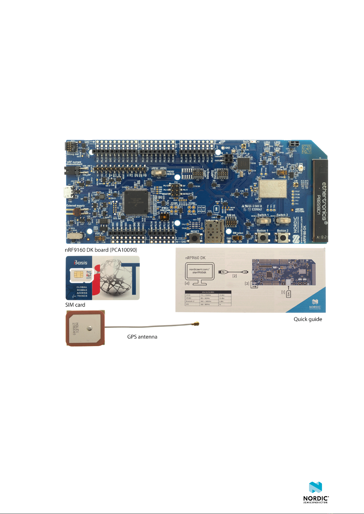
2Kit content.................................... 8
2.1 Hardware content ................................ 8
3Operating modes................................ 9
3.1 Firmware development mode ........................... 9
3.1.1 Device programming ............................. 9
3.1.2 Virtual COM port ............................... 9
3.1.3 MSD ....................................10
3.1.4 Reset ................................... 10
3.2 Performance measurement mode ......................... 11
3.2.1 USB detect ................................. 11
4Hardware description............................. 13
4.1 Block diagram ................................. 13
4.2 Hardware figures ................................ 13
4.3 Power supply ..................................14
4.3.1 nRF9160 supply ............................... 16
4.3.2 VDD supply rail ............................... 16
4.3.3 Other power domains ............................ 17
4.4 Antenna interfaces ............................... 17
4.5 GPS ...................................... 17
4.6 GPIO interfaces ................................. 18
4.7 nRF52840 ................................... 20
4.7.1 nRF9160 DK board control .......................... 21
4.7.2 Bluetooth/IEEE 802.15.4 network processor ................... 22
4.8 Buttons, slide switches, and LEDs ......................... 23
4.9 Debug input and trace options .......................... 24
4.10 Debug output ................................. 25
4.10.1 Connectors for programming external boards .................. 26
4.11 Signal routing switches ............................. 27
4.11.1 Interface MCU disconnect switches ...................... 27
4.11.2 Switches for UART interface ......................... 28
4.11.3 Switches for buttons and LEDs ........................ 29
4.11.4 Switches for nRF52840 interface ....................... 31
4.12 SIM and eSIM ................................. 32
4.13 Additional interfaces .............................. 33
4.14 SiP enable .................................. 34
4.15 Solder bridge configuration ........................... 34
5Measuring current............................... 36
5.1 Preparing the development kit for current measurements ............... 36
5.2 Using an oscilloscope for current profile measurement ................ 37
5.3 Using a current meter for current measurement ................... 37
4418_1216 v0.9.1 ii

Revision history
Date Version Description
March 2020 0.9.1 • Updated Related documentation on page 6
• Updated Debug output on page 25
• Added Connectors for programming external boards on page
26
October 2019 0.9 Updated to match DK v0.9.0
• Updated:
•Hardware content on page 8
•Related documentation on page 6
•Firmware development mode on page 9
•Performance measurement mode on page 11
•Block diagram on page 13
•Hardware figures on page 13
•Power supply on page 14
•Antenna interfaces on page 17
•GPS on page 17
•nRF9160 DK board control on page 21
•SIM and eSIM on page 32
•Additional interfaces on page 33
•Solder bridge configuration on page 34
•Preparing the development kit for current measurements on
page 36
• New:
•Interface MCU disconnect switches on page 27
•Switches for UART interface on page 28
•Switches for nRF52840 interface on page 31
• Removed:
• Getting started
July 2019 0.7.2 Updated:
•nRF9160 supply on page 16
March 2019 0.7.1 Updated to match DK v0.8.5:
•Hardware content on page 8
•nRF9160 supply on page 16
•Antenna interfaces on page 17
•GPS on page 17
•nRF9160 DK board control on page 21
•Solder bridge configuration on page 34
•Preparing the development kit for current measurements on
page 36
•RF measurements on page 39
4418_1216 v0.9.1 iv

Revision history
Date Version Description
•Radiated performance of nRF9160 DK on page 40
December 2018 0.7 Updated to match DK v0.8.2
November 2018 0.5.1 Preview DK changed into DK
October 2018 0.5 First release
Previous versions
PDF files for the previous versions are available here:
•nRF91 DK User Guide v0.9
•nRF91 DK User Guide v0.7.2
•nRF91 DK User Guide v0.7.1
•nRF91 DK User Guide v0.7
4418_1216 v0.9.1 v

1Introduction
The nRF9160 DK is a hardware development platform used to design and develop application firmware on
the nRF9160 LTE Cat-M1 and Cat-NB1 System in Package (SiP).
The DK (Development Kit) includes all necessary external circuitry like a SIM card holder and an antenna
and it provides developers access to all I/O pins and relevant module interfaces.
Note: The DK can be connected to a base station by the onboard LTE antenna or to an LTE
emulator by an RF cable. See our nRF9160 certifications webpage to find the bands supported by
the LTE modem. Without a UICC/SIM connected, the DK cannot initiate communication with the
LTE network.
The key features of the development kit are:
• nRF9160 SiP
• LTE antenna that supports all bands supported by the SiP
•Global Positioning System (GPS) antenna
• nRF52840 as a board controller and network processor for Bluetooth® and IEEE 802.15.4 protocols
• Buttons, switches, and LEDs for user interaction
• I/O interface for Arduino form factor plug-in modules
• SEGGER J-Link OB Debugger with debug out functionality
• UART interface through virtual COM port
• USB connection for debug/programming and power
• SIM card socket for nano-SIM (4FF SIM)
• Interfaces for nRF9160 current consumption measurements
Note: nRF9160 DK is compliant with the PS1 classification according to the IEC 62368-1 standard.
Skilled person: Person with relevant education or experience to enable him or her to identify hazards and
to take appropriate actions to reduce the risks of injury to themselves and others.
1.1 Related documentation
In addition to the information in this document, you may need to consult other documents.
4418_1216 v0.9.1 6

2Kit content
The nRF9160 DK includes hardware, preprogrammed firmware, documentation, hardware schematics, and
layout files.
2.1 Hardware content
The nRF9160 DK v0.9.x contains the development kit board PCA10090, a GPS antenna, and a SIM card.
Figure 1: nRF9160 DK v0.9.x kit content
Hardware files
The hardware design files including schematics, PCB layout files, bill of materials, and Gerber files for the
nRF9160 DK are available on the product page, nRF91 SiP Series.
4418_1216 v0.9.1 8

3Operating modes
The nRF9160 DK has various modes of operation.
3.1 Firmware development mode
The firmware development mode is the default with the IFMCU DISCONN switch (SW1) in the left position.
The primary interface for programming and debugging the nRF9160 DK is the USB port (J4). The USB port
is connected to an interface MCU which embeds a SEGGER J-Link-OB (On Board) debug probe.
Figure 2: nRF9160 DK firmware development mode
3.1.1 Device programming
The nRF9160 DK supports SWD programming interfaces for both onboard and off-board nRF targets.
The primary target for programming and debugging in the DK is the nRF9160. The interface MCU also
supports programming the onboard nRF52840 as well as external nRF devices fitted on a shield or through
a connector to external boards such as the user's own prototypes.
The interface MCU will automatically detect if external targets are plugged in. The PROG/DEBUG switch
(SW5) is used to select nRF9160 or nRF52840 for programming or debugging on board. Note that there
are significant limitations on using the nRF52840 on the nRF9160 DK. For more information, see nRF9160
DK board control on page 21.
3.1.2 Virtual COM port
The interface MCU also features three UART interfaces through three virtual COM ports.
The virtual COM ports are the following:
• VCOM0 – Connected to nRF9160 (default)
• VCOM1 – Connected to nRF52840 (nonconfigurable)
• VCOM2 – Not connected to nRF9160 (default)
For details on routing VCOM0 and VCOM2, see nRF9160 DK board control on page 21.
The virtual COM ports have the following features:
• Flexible baud rate settings up to 1 Mbps
• RTS/CTS-style Hardware Flow Control (HWFC) handling
4418_1216 v0.9.1 9

Operating modes
The table below shows an overview of the GPIOs used for the UART connections on the nRF9160 and
nRF52840:
nRF91 APP1 nRF91 APP2 nRF52840
TXD P0.29 P0.01 P0.03
RXD P0.28 P0.00 P0.05
CTS P0.26 P0.15 P0.07
RTS P0.27 P0.14 P1.08
Table 1: GPIOs used for virtual COM ports on nRF9160 and nRF52840
Note:
• Baud rate 921 600 is not supported through the virtual COM port.
3.1.3 MSD
The interface MCU features a mass storage device (MSD). This makes the DK appear as an external drive
on your computer.
This drive can be used for drag-and-drop programming. However, files cannot be stored on this drive. By
copying a HEX file to the drive, the interface MCU will program the file to the device. The J-Link OB will
program the target that is selected with the nRF52/nRF91 switch (SW5). For limitations on nRF52840 use,
see nRF9160 DK board control on page 21.
Note:
• Windows might try to defragment the MSD part of the interface MCU. If this happens, the
interface MCU will disconnect and become unresponsive. To return to normal operation, the
development kit must be power cycled.
• Your antivirus software might try to scan the MSD part of the interface MCU. Some antivirus
programs trigger a false positive alert in one of the files and quarantine the unit. If this happens,
the interface MCU will become unresponsive.
• If your computer is set up to boot from USB, it can try to boot from the development kit if the
development kit is connected during boot. This can be avoided by unplugging the development
kit before a computer restart or changing the boot sequence of the computer.
You can also disable the MSD of the kit by using the msddisable command in J-Link Commander.
To enable, use the msdenable command. These commands take effect after a power cycle of the
development kit and stay this way until changed again.
3.1.4 Reset
The nRF9160 DK is equipped with a RESET button (SW2).
By default, the RESET button is connected to the interface MCU that will forward the reset signal to the
nRF9160 or nRF52840, depending on the state of the nRF52/nRF91 switch. If IF MCU DISCONNECT is
activated, the RESET button will be connected to the nRF9160 directly.
4418_1216 v0.9.1 10

Operating modes
3.2 Performance measurement mode
The performance measurement mode can be selected by moving the IFMCU DISCONN switch (SW1) to the
right position, which disconnects the interface MCU from the nRF9160 SiP using analog switches.
This is done to isolate the nRF9160 SiP as much as possible and can be of use when measuring currents on
low-power applications.
Figure 3: nRF9160 DK performance measurement mode
The development kit detects if there is a USB cable plugged in (see USB detect on page 11) and will
disconnect and power down the interface MCU when another supply than the USB is used. If the USB
connector is used for power supply only (USB battery back) you can also disable the interface MCU using
SW1.
USB detect and SW1 also control the routing of the RESET signal from the RESET button (SW2). Normally, it
is routed through the interface MCU, but if that is disabled, the reset button will be routed directly to the
nRF9160 SiP.
There are also a number of other reset routing options available through the use of solder bridges:
• When the interface MCU is disconnected, the RESET button is connected to pin 32 (nRESET) of the
nRF9160 SiP. The RESET button can be disconnected from the nRF9160 SiP by cutting SB25.
• When the interface MCU is disconnected, shorting SB29 will connect the RESET pin of the Arduino
interface to the reset pin of the nRF9160 SiP.
• When the interface MCU is connected, shorting SB30 will connect the RESET pin of the Arduino
interface to the BOOT input of the interface MCU.
• Shorting SB27 will connect the RESET pin of the Arduino interface to the RESET button.
• Shorting SB28 will connect the RESET pin of the Arduino interface to the nRESET pin of the nRF9160 SiP.
3.2.1 USB detect
To detect when the USB for the interface MCU is connected, there is a circuit sensing the VBUS of USB
connector J4.
When the USB cable is connected, the VDD is propagated to the USB_DETECT signal.
4418_1216 v0.9.1 11

Operating modes
Figure 4: USB detect switch
4418_1216 v0.9.1 12

4Hardware description
The nRF9160 DK features an onboard programming and debugging solution.
4.1 Block diagram
The block diagram shows the main functionality of the nRF9160 DK.
nRF9160
GPS LNA/
BPF
Analog switch
Analog
switches
nRF52840
Analog
switches
Debug in
VDD IO switch Power switch
Power supply
circuitry
Interface MCU
IF MCU
Disconnect
switch
Debug out
Reset button
USB
connector
External
supply
LTE antenna
SIM
eSIM
(not mounted)
Prog. switch
Debug in
GPS antenna
2.4 GHz
antenna
LEDs
Buttons/
Switches
Connector
interface
U.FL
connector
Analog switch
Analog
switches
SWF
connector
SWF
connector
Antenna
select switch
SIM select
switch
Figure 5: nRF9160 DK block diagram
4.2 Hardware figures
The nRF9160 DK hardware drawings show both sides of the PCA10090 board.
4418_1216 v0.9.1 13

Hardware description
Figure 6: nRF9160 DK (PCA10090), front view
Figure 7: nRF9160 DK board (PCA10090), back view
4.3 Power supply
nRF9160 DK has a flexible and configurable power supply system to allow software development and
testing using different power sources and to facilitate accurate power measurements.
The power source options are:
• USB connector J4 (5 V)
• External supply on P28 (3.0 V–5.5 V)
• VIN 3–5 V on P15 (3.0 V–5.5 V)
Figure 8: nRF9160 DK power supply options
4418_1216 v0.9.1 14

Hardware description
Figure 9: Power sources and switches
4418_1216 v0.9.1 15

Hardware description
To ensure that only one of the power sources are used on the board at a time, power switches are
implemented on each of them as shown in Figure 9: Power sources and switches on page 15. These
switches prioritize the supply sources in the following manner:
1. USB
2. P15
3. P28
This means that if power is connected to more than one the interfaces, the higher priority interface will be
chosen to supply the board.
The supply voltage is then routed through the ON/OFF switch (SW9) to the common rail VSUPPLY, which
acts as the source for the supply voltage regulators for the circuitry on the board.
The supply flows from VOUT to VIN, which is correct. The body diode of the internal transistor powers the
VSUPPLY net, which supplies the gates controlling the enable signal of the switches.
The power switches will introduce a small voltage drop between the power source connected to the board
and the VSUPPLY. To avoid this, the power switches can be bypassed by shorting one of the solder bridges
as shown in the table:
Power source Power switch bypass Voltage level
USB connector (J4) SB24 5 V
External supply (P28) SB36 3.0 V–5.5 V
VIN 3–5 V (P15) SB4 3.0 V–5.5 V
Table 2: Bypassing power switch
Note: Connect only one power source at a time in this case. Shorting the solder bridges removes
the reverse voltage protection.
4.3.1 nRF9160 supply
The nRF9160 has a supply range of 3.0–5.5 V and is therefore powered by the VSUPPLY rail directly.
4.3.2 VDD supply rail
VDD is the main supply for the rest of the circuitry on the board. It is regulated down from VSUPPLY by a
buck regulator (U22).
Figure 10: VDD buck regulator and selection switch
4418_1216 v0.9.1 16

Hardware description
You can set the VDD voltage to 1.8 V (default) or 3 V with SW11. Running 3 V GPIO with heavy load may
degrade the LTE RF performance. A third option for customizing VDD voltage level is applying a custom
voltage level to VIO_REF (P15). For more information, see GPIO - General purpose input/output in the
nRF9160 Objective Product Specification.
VDD powers most of the other circuits and will set the GPIO signal amplitude between nRF9160 and other
circuits on the board including connectors and PIN headers.
4.3.3 Other power domains
The interface MCU needs a 3.0 V for its USB interface supply, a low-dropout voltage regulator (U32) is used
for this. This regulator also supplies the LEDs on the board, giving these a fixed supply.
4.4 Antenna interfaces
nRF9160 DK has three antenna interfaces mounted representing LTE, GPS, and the 2.4 GHz radio.
The LTE and 2.4 GHz RF signals are propagated through two coaxial connectors with switches that will
disconnect the corresponding antenna from the radio if adapter cables are connected. This makes it
possible to perform conducted measurements or attach external antennas to the radio.
The GPS signal is RX only. There is a Low-Noise Amplifier (LNA) and a Band-Pass Filter (BPF) that amplify
and filter the signal before it is fed to the GPS RF port on the nRF9160. Switch SW12 controls if the input
signal to the LNA is connected to RF connector P29 or if the signal is routed from the GPS antenna A2
through switch U33. The LNA is connected to the GPS antenna by default.
The relation between the connectors, radios, and antennas are the following:
•J1 – Connector with a switch for the LTE antenna (A1)
•J7 – Connector with a switch for the 2.4 GHz antenna (A3)
•P29 – Connector for an external GPS antenna
For more details of the GPS antenna interface, see GPS on page 17.
4.5 GPS
The nRF9160 has a dedicated GPS port to support global navigation.
The GPS signal is received either from the onboard or an external GPS antenna. The onboard antenna (A2)
is connected to the combined LNA and BPF U3 through switches U33 and U34.
Figure 11: Onboard GPS antenna (A2), LNA/BPF (U3), connector P29, and switch SW12
4418_1216 v0.9.1 17

Hardware description
The onboard antenna can be disconnected and an external GPS antenna enabled by attaching the external
GPS antenna to connector P29 and sliding switch SW12 to CON position. 3.0 V DC is fed through P29 to
supply an external LNA, if desired. The external GPS antenna can be connected to connector P29 (Hirose
part no. U.FL-R-SMT-1). A compatible adapter cable is required to connect a GPS antenna to the DK.
Switch U34 and the combined LNA and BPF are enabled by the GPS-enable signal from the nRF9160.
The signal is next amplified and filtered in the LNA and BPF U3 before it is fed to the nRF9160. This makes
the GPS receiver more sensitive to GPS signals and less sensitive to interference from other sources on the
DK or nearby.
Note:
• GPS signals do not usually penetrate ceilings or other structures that well. Therefore, for best
GPS performance, the DK should be placed on a flat surface in an open space outside, far from
sources of interference and other structures that may block the signals from space.
• This functionality is only available if the modem firmware used in the nRF9160 supports GPS.
• The Molex patch antenna achieves the highest gain when placed horizontally on a surface (x-y)
facing the z-axis since it can receive all propagated GPS signals. A lower gain will be experienced
if the patch antenna is mounted on a surface is at an angle with the horizontal surface.
Figure 12: GPS connected to the nRF9160
4.6 GPIO interfaces
Access to the nRF9160 GPIOs is available from connectors P7, P10, P14, P19, and P27. The nRF9160 DK
supports the Arduino UNO interface.
4418_1216 v0.9.1 18

Hardware description
Figure 13: Access to nRF9160 GPIOs
GPIO signals are also available on connectors P5, P6, P12, P17, and P25, which are on the bottom side of
the board. By mounting pin lists on the connector footprints, the nRF9160 DK can be used as a shield for
Arduino motherboards.
For easy access to GPIO, power, and ground, the signals can also be found on the through-hole connectors
P8, P12, P17, and P25.
Note: GPIO P0.29 is not available on any through-hole connector.
GPIO nRF9160 DK Function
P0.00, P0.01, P0.14, and P0.15 Used as a second UART connection to the interface MCU.
For more information, see Virtual COM port on page 9.
P0.02, P0.03, P0.04, P0.05, P0.06, P0.07,
P0.08, and P0.09
Connected by default to buttons, slide switches, and LEDs.
For more information, see Buttons, slide switches, and
LEDs on page 23.
P0.17, P0.18, P0.19, P0.21, P0.22, P0.23,
COEX0, COEX1, and COEX2
Used to connect the nRF9160 to the nRF9160 DK board
control on page 21.
P0.26, P0.27, P0.28, and P0.29 Used as the primary UART connection to the interface
MCU. For more information, see Virtual COM port on page
9.
Table 3: Default pin settings
4418_1216 v0.9.1 19
Other manuals for nRF9160
2
Table of contents