Samsung KCT52A Installation guide

l
SAMSUNG GROUP
l
SAMSUNG GROUP
OO]
TOC1
CTVTraining Manual
KCT52A Chassis
20 Inch: TXE2045,TXE2046
25 Inch: TXE2545,TXE2546,TXE2549
27 Inch: TXE2745,TXE2746,TXE2749
Samsung Electronics America
Product Support Department.
l

l
SAMSUNGGROUP
l
SAMSUNGGROUP
O[O]
TOC 2
Contents
Block Diagrams
Power Supply Circuit
IC Block Diagram & Pin Description
ICPin Voltage & Waveforms
Power Supply Description
Troubleshooting – No Raster and No Sound
Micom Circuit
IC Pin Description
MICOM (IC901) Pin Description
EEPROM (IC902) Pin Description
IC Pin Voltage & Waveforms
Tuner Circuit
Tuner Description
IF/Chroma/Video Circuit
IC Pin Description
IC Pin Voltage & Waveforms
Troubleshooting – No Color
Horizontal Deflection Circuit
Horizontal Deflection Circuit Description
Vertical Deflection Circuit
Vertical Deflection Circuit Description
Troubleshooting –No Vertical Scan (Horizontal Line)
Sound Circuit
IC Block Diagram & Description
Troubleshooting – No Sound
CRT Drive Circuit
CRT Drive Circuit Description
Troubleshooting – No Raster (Sound OK)
A/V Switching Description
PIP Block Diagram
Schematic Diagram
PIP Principle Sync Timing Diagrams
Alignment and Adjustment
Preadjustment
Factory (Service) Mode
Other Adjustments

KCT52A Chassis
l
SAMSUNG GROUP
l
SAMSUNG GROUP
O[O]
TOC 3
Block Diagrams

KCT52A Chassis
l
SAMSUNG GROUP
l
SAMSUNG GROUP
O[O]
TOC 4
Power Supply Circuit

KCT52A Chassis
l
SAMSUNG GROUP
l
SAMSUNG GROUP
O[O]
TOC 5
Power Supply Circuit

KCT52A Chassis
l
SAMSUNG GROUP
l
SAMSUNG GROUP
O[O]
TOC 6
IC Block Diagram & Pin Description
IC801 (STRS6709)
Block Diagram
IC801 (STRS6709) Pin Description
Pin No Pin Name Description
1 Collector Switching TR Collector
2 GND Switching TR Emitter
3 Base Switching TR Base
4 Sink Control S/TR base current
5 Drive Supply S/TR base current
6 OCP Over current Protection
7 Feedback Output voltage Feedback
8 Inhibit Off time control, latch up control
9 B+ Main Power Supply
IC801 (STRS6709) Internal Parameter
R1 T-on trimming C1 3300 pF
R2 T-off trimming C2 0.01 uF
R3 1 K ohm C3 820 pF
R4 0.7 ohm C4 0.01 uF
R5 100 ohm
R6 85 ohm

KCT52A Chassis
l
SAMSUNG GROUP
l
SAMSUNG GROUP
O[O]
TOC 7
IC Pin Voltage & Waveforms
IC801 Pin Voltage & Waveform
Pin No Stand-by Power On
1 See printout See printout
2 See printout See printout
3 See printout See printout
4 See printout See printout
5 See printout See printout
6 See printout See printout
7 See printout See printout
8 See printout See printout
9 6V See printout
HC801 Pin Voltage & Waveform
Pin No Stand-by Power On
1 See printout See printout
2 See printout See printout
3 See printout See printout
5 See printout See printout
6 6V See printout
HC802 Pin Voltage & Waveform
Pin No Stand-by Power On
1 0 V 0 V
2 11.1 V 12.5 V
3 0 V 5 V
4 12.5 71 V
6 15 V 72.2 V

KCT52A Chassis
l
SAMSUNG GROUP
l
SAMSUNG GROUP
O[O]
TOC 8
IC Pin Voltage & Waveforms
IC852 Pin Voltage & Waveform
Pin No Stand-by Power On
1 37 V 129 V
2 10.8 V 12.5 V
IC802 Pin Voltage & Waveform
Pin No Stand-by Power On
1 11.4 V 12.2 V
2 13.1 V 13.7 V
3 2.9 V 3 V
4 0 V 3.8 V
6 4.7 V 4.7 V
8 0 V 8 V
9 5 V 5 V
Output2 (Pin 8) is disabled if Pin 4 is less than 0.8 V.
The /Reset (Pin 6) goes low if output1(Pin 9) is less
than 4.85 V, and goes high if Pin 9 is higher than 4.9 V.
The cap. C810 connected to Pin 3 determines delay
time (Td) of /Rest Pin going high or low.
HC853 Pin Voltage & Waveform
Pin No Stand-by Power On
1 12.9 V 13.7 V
2 0.6 V 11.8 V
4 0 V 3.8 V

KCT52A Chassis
l
SAMSUNG GROUP
l
SAMSUNG GROUP
O[O]
TOC 9
Power Supply Description Start up Circuit
When AC cord is plugged in, the initial current starts flowing
through the path as shown, and charges C852.
When Vin reaches about 8V, the control circuit is activated,
and the oscillation begins.
D1, D2 windings provide the necessary back-up current to Vin
after the control circuit is activated as the initial current alone
can not sustain the current consumed by the control IC.
The DI winding voltage is set between the threshold of Stop
voltage (Vin=5.1 V) and Overvoltage (Vin=10V).
As shown in the graph, D1 and D2 winding voltages are
necessary to power up the control IC.

KCT52A Chassis
l
SAMSUNG GROUP
l
SAMSUNG GROUP
O[O]
TOC 10
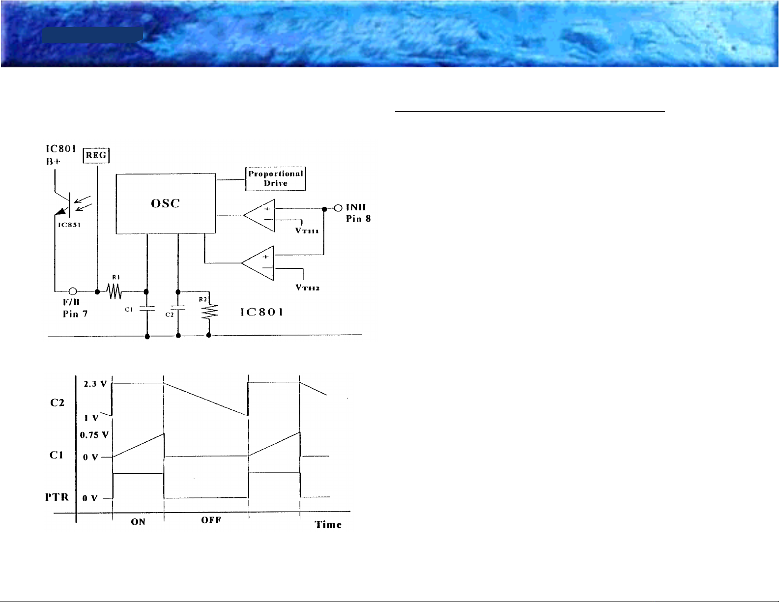
Power Supply Description On-Time Control Circuit Description
The oscillator generates driving pulses to turn PTR on/off by
charging and discharging C1 and C2.
Refer to the waveform shown below, left.
When the PTR is on, C2 is charged to the constant voltage.
Al the same time, C1 starts charging at almost 0 V through
R1. When the voltage of C1 approaches 0.7V, the output of
oscillator is reversed and the PTR is turned off.
As the PTR is turned off, C1 is rapidly discharged by the
oscillator, and C2 starts to discharge through R2.
When the voltage of C2 decreases to approx. 1V, the output of
the oscillator reverses again and the PTR turned on.
On-time control is done by changing C1 charging rate through
feedback current developed in the photo coupler, which
depends on the input voltage and load current fluctuations.
Fig. 1
Fig. 2

KCT52A Chassis
l
SAMSUNG GROUP
l
SAMSUNG GROUP
O[O]
TOC 11
Power Supply Description Off-Time Control Circuit Description
The INH voltage is used as the input signal to the COMP1
and COMP2 within the control IC.
When INH voltage reaches Vth1, the OSC output is kept low,
so PTR maintains off mode. (Fig. 1)
When INII voltage reaches Vth2, the output of the COMP2
reverses and tile voltage of C2 starts to discharge rapidly. If
the INH voltage does not fall below Vth2, tile C2 voltage will
be kept to almost 0 V, and tile PTR will remain off mode.
(Fig.2)
When the PTR is off, the primary energy is transferred to the
secondaries including DI winding, which voltage is set to
higher volatile than Vth2 in normal operation.
This transferred energy starts charging Cinh through D3 and
Rinh. When INH voltage reaches Vth, C2 will discharge
quickly, and remain low even after the energy transfer is com-
pleted became the INH voltage does not fall instantaneously,
bid rather fall in decay fashion. This falling time duration
depends on Cinh,IC input impedance, mid INH voltage,
which is proportional to output load voltage.
Higher the load voltage (less load current) is, the longer the
falling time is because INH voltage is higher.
Fig. 1
Fig. 1

KCT52A Chassis
l
SAMSUNG GROUP
l
SAMSUNG GROUP
O[O]
TOC 12
Power Supply Description PTR Drive Circuit Description
The control IC uses a proportional drive system to reduce the
PTR ON loss, saturation loss, and storage time loss.
When Proprot. drive circuit generates a positive pulse out of
Pin 5, the base current to Pin 3 (base of PTR) develops, and
increases linearly because of R813 and C851 combination.
This base current drives PTR to turn on.
When the driving pulse goes low, the R813 and C851 combi-
nation reverse biases PTR base completely to make sure the
the PTR is off.
The relation between Vbe (IB) and Vce (Ic) of the PTR is
shown on the graph.

KCT52A Chassis
l
SAMSUNG GROUP
l
SAMSUNG GROUP
O[O]
TOC 13
Power Supply Description OCP (Over Current Protection)
Circuit Description)
The overcurrent protection is performed by the pulse-by-pulse
system, which directly detects the collector current of the
PTR.
The detect reference voltage to the comparator is set to -1 V
above the control IC ground (Pin 2).

KCT52A Chassis
l
SAMSUNG GROUP
l
SAMSUNG GROUP
O[O]
TOC 14
Power Supply Description
Over Voltage Protection Circuit Description
The overvoltage protection circuit activates the latch circuit
when the Vin voltage exceeds about 11V.
Since Vin is proportional to the load voltage, the OVP circuit
will trigger the latch circuit when an abnormally high voltage
appears on the load line due to the open loop in the feedback
path.
Overheat Protection Circuit Description
When the control IC's temperature reaches over 150 degree C,
the latch circuit is activated.
Actual temperature detection is done through the control cir-
cuit mounted on the IC frame internally.
Latch Circuit Description
The latch circuit stops oscillation of the control IC when OVP
or Overheat condition occurs.
When this happens, the Vin voltage will fluctuate between the
Stop voltage and the Operation voltage continuously.

KCT52A Chassis
l
SAMSUNG GROUP
l
SAMSUNG GROUP
O[O]
TOC 15
(POWER ON) IC801 PIN 1
(POWER ON) IC801 PIN 3
(POWER ON) IC801 PIN 2
(POWER ON) IC801 PIN 4

KCT52A Chassis
l
SAMSUNG GROUP
l
SAMSUNG GROUP
O[O]
TOC 16
(POWER ON) IC801 PIN 5
(POWER ON) IC801 PIN 7
(POWER ON) IC801 PIN 6
(POWER ON) IC801 PIN 8

KCT52A Chassis
l
SAMSUNG GROUP
l
SAMSUNG GROUP
O[O]
TOC 17
(POWER ON) IC801 PIN 9
(STAND-BY) IC801 PIN 2
(STAND-BY) IC801 PIN 1
(STAND-BY) IC801 PIN 3

KCT52A Chassis
l
SAMSUNG GROUP
l
SAMSUNG GROUP
O[O]
TOC 18
(POWER ON) IC801 PIN 4
(STAND-BY) IC801 PIN 6
(STAND-BY) IC801 PIN 5
(STAND-BY) IC801 PIN 7

KCT52A Chassis
l
SAMSUNG GROUP
l
SAMSUNG GROUP
O[O]
TOC 19
(POWER ON) IC801 PIN 8
(POWER ON) IIC801 PIN 1
(STAND-BY) IC801 PIN 9
(POWER ON) IIC801 PIN 2

KCT52A Chassis
l
SAMSUNG GROUP
l
SAMSUNG GROUP
O[O]
TOC 20
(POWER ON) IIC801 PIN 3
(STAND-BY) IIC801 PIN 1
(POWER ON) IIC801 PIN 5
(STAND-BY) IIC801 PIN 2
Table of contents
Popular Chassis manuals by other brands

Svive
Svive LUNA X750 manual

Allied Telesis
Allied Telesis SwitchBlade AT-SB4104-00 Quick install guide

Juniper
Juniper CTP1000 Series Hardware guide

Fortinet
Fortinet FortiGate-7000F Series System guide

TKH
TKH Optelecom 9000 Series Installation and operation manual

Keysight Technologies
Keysight Technologies M9010A PXIe user guide