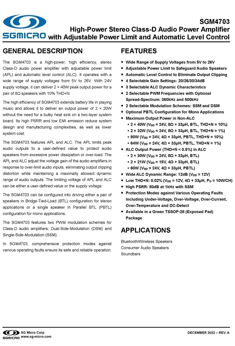
SG Micro SGM4700 User manual

SGM4700
High-Power Stereo Class-D Audio Power Amplifier
with Adjustable Power Limit and Automatic Level Control
SG Micro Corp
www.sg-micro.com
NOVEMBER 2023 – R EV. A. 1
GENERAL DESCRIPTION
The SGM4700 is a high-power, high efficiency, stereo
Class-D audio power amplifier with adjustable power limit
(APL) and automatic level control (ALC). It operates with a
wide range of supply voltages from 5V to 20V. With 15V
supply voltage, it can deliver 2 × 23W output power for a pair
of 4Ω speakers with 1% THD+N, or an ALC output power of 2
× 20W with THD+N less than 0.5%.
The high efficiency of SGM4700 extends battery life in playing
music and allows it to deliver an output power of 2 × 20W
without the need for a bulky heat sink on a two-layer system
board. Its high PSRR and low EMI emission reduce system
design and manufacturing complexities, as well as lower
system cost.
The SGM4700 features APL and ALC. The APL limits peak
audio outputs to a user-defined value to protect audio
speakers from excessive power dissipation or over-load. The
APL and ALC adjust the voltage gain of the audio amplifiers in
response to over-limit audio inputs, eliminating output clipping
distortion while maintaining a maximally allowed dynamic
range of audio outputs. The limiting voltage of APL and ALC
can be either a user-defined value or the supply voltage.
The SGM4700 can be configured into driving either a pair of
speakers in Bridge-Tied-Load (BTL) configuration for stereo
applications or a single speaker in Parallel BTL (PBTL)
configuration for mono applications.
The SGM4700 features two PWM modulation schemes for
Class-D audio amplifiers: Dual-Side-Modulation (DSM) and
Single-Side-Modulation (SSM).
In SGM4700, comprehensive protection modes against
various operating faults ensure its safe and reliable operation.
FEATURES
●Wide Range of Supply Voltages from 5V to 20V
●Adjustable Power Limit to Safeguard Audio Speakers
●Automatic Level Control to Eliminate Output Clipping
●4 Selectable Gain Settings: 20/26/30/34dB
●3 Selectable ALC Dynamic Characteristics
●2 Selectable PWM Frequencies with Optional
Spread-Spectrum: 360kHz and 500kHz
●2 Selectable Modulation Schemes: SSM and DSM
●Optional PBTL Configuration for Mono Applications
●Maximum Output Power (THD+N = 1%) in Non-ALC
2 × 32W (VDD = 18V, 4Ω + 33μH, BTL)
2 × 18W (VDD = 18V, 8Ω + 33μH, BTL)
33W (VDD = 15V, 3Ω + 15μH, PBTL)
●Maximum Output Power (THD+N < 0.5%) in ALC
2 × 29W (VDD = 18V, 4Ω + 33μH, BTL)
2 × 16W (VDD = 18V, 8Ω + 33μH, BTL)
30W (VDD = 15V, 3Ω + 15μH, PBTL)
●Wide ALC Dynamic Range: 12dB (VDD = 12V)
●Low THD+N: 0.02% (VDD = 12V, 4Ω + 33μH, PO= 10W/CH)
●High PSRR: 80dB at 1kHz with SSM
●Protection Modes against Various Operating Faults
Including Under-Voltage, Over-Voltage, Over-Current,
Over-Temperature and DC-Detect
●Available in a Green TSSOP-28 (Exposed Pad)
Package
APPLICATIONS
Bluetooth/Wireless Speakers
Consumer Audio Speakers
Soundbars

High-Power Stereo Class-D Audio Power Amplifier
SGM4700 with Adjustable Power Limit and Automatic Level Control
2
NOVEMBER 2023
SG Micro Corp
www.sg-micro.com
PACKAGE/ORDERING INFORMATION
MODEL PACKAGE
DESCRIPTION
SPECIFIED
TEMPERATURE
RANGE
ORDERING
NUMBER
PACKAGE
MARKING
PACKING
OPTION
SGM4700 TSSOP-28
(Exposed Pad) -40℃to +85℃SGM4700YPTS28G/TR
SGM4700
YPTS28
XXXXX
Tape and Reel, 4000
MARKING INFORMATION
NOTE: XXXXX = Date Code, Trace Code and Vendor Code.
Trace Code
Vendor Code
Date Code - Year
X XXX X
Green (RoHS & HSF): SG Micro Corp defines "Green" to mean Pb-Free (RoHS compatible) and free of halogen substances. If
you have additional comments or questions, please contact your SGMICRO representative directly.
ABSOLUTE MAXIMUM RATINGS
Supply Voltage Pins
AVDD, PVDD .................................................. -0.3V to 26V
Digital I/O Pins
EN, FAULTB ..................................... -0.3V to VAVDD +0.3V
MODS ............................................... -0.3V to VGVDD +0.3V
Analog Output Pins
GVDD ............................................................ -0.3V to 6.5V
ALC, GAIN, FREQ ............................ -0.3V to VGVDD +0.3V
Analog Input Pins
INPL/R, INNL/R, PLIMIT ................... -0.3V to VGVDD +0.3V
Package Thermal Resistance
TSSOP-28 (Exposed Pad), θJA .................................. 28℃/W
Junction Temperature.................................................+150℃
Storage Temperature Range ....................... -65℃to +150℃
Lead Temperature (Soldering, 10s) ............................+260℃
ESD Susceptibility
HBM............................................................................. 1500V
CDM ............................................................................ 1000V
OVERSTRESS CAUTION
Stresses beyond those listed in Absolute Maximum Ratings
may cause permanent damage to the device. Exposure
to
absolute maximum rating conditions for extended periods
may affect reliability. Functional operation of the device at any
conditions beyond those indicated in the Recommended
Operating Conditions section
is not implied.
ESD SENSITIVITY CAUTION
This integrated circuit can be damaged if ESD protections are
not considered carefully. SGMICRO recommends that all
integrated circuits be handled with appropriate precautions.
Failure
to observe proper handling
and installation procedures
can cause damage. ESD damage can range from subtle
performance
degradation to
complete device failure. Precision
integrated circuits may be more susceptible to damage
because even small parametric changes could cause the
device not to meet the published specifications.
DISCLAIMER
SG Micro Corp reserves the right to make any change in
circuit
design, or specifications
without prior notice.

High-Power Stereo Class-D Audio Power Amplifier
SGM4700 with Adjustable Power Limit and Automatic Level Control
3
NOVEMBER 2023
SG Micro Corp
www.sg-micro.com
RECOMMENDED OPERATING CONDITIONS
PARAMETER SYMBOL CONDITIONS MIN TYP MAX UNITS
Supply Voltage Range (1, 2) VDD PVDD, AVDD 5 20 V
Operating Ambient Temperature TA-40 +85 ℃
Minimum Load Impedance (3) RLBTL Configuration (Stereo) 4 Ω
PBTL Configuration (Mono) 3
Audio Input Capacitor CIN At INPL/R, INNL/R 1 µF
Maximum Audio Input Voltage Level
VIN, MAX At INNL/R, INPL/R 2.0 VRMS
PLIMIT Voltage Range VPLIMIT PLIMIT 0 VGVDD V
Maximum Load Current at GVDD ILOAD 5 mA
Supply Decoupling Capacitor
CPVDD Ceramic 1
µF
Electrolytic or Tantalum
(4)
220
CAVDD Ceramic 1
CGVDD Ceramic 1
CPLIMIT Ceramic 0.1
Bootstrap Holding Capacitor CBAt BSTPL/R, BSTNL/R 0.33 0.47 0.68 µF
Mono Mode Select INNR INPR PBTL Configuration Both Pins Shorted to GND
Modulation Scheme Select MODS Single-Side-Modulation (SSM) Low or Open
Double-Side-Modulation (DSM) High
Voltage Gain Select GAIN
26dB Open
30dB Shorted to GND
34dB 68kΩ to GND
20dB 300kΩ to GND
ALC Mode Select ALC
Non-ALC Open
ALC-1 Shorted to GND
ALC-2 68kΩ to GND
ALC-3 300kΩ to GND
PWM Frequency Select FREQ
Constant Frequency at 360kHz Open
360kHz with Spread-Spectrum Shorted to GND
Constant Frequency at 500kHz 68kΩ to GND
500kHz with Spread-Spectrum 300kΩ to GND
NOTES:
1. The peak supply voltage including its tolerance over various operating conditions must not exceed its absolute-maximum-rated value (26V).
Exposure to absolute-maximum-rated supply voltage may damage the device or affect device reliability permantly.
2. For high power applications, the maximum power supply VDD that can be applied to the SGM4700 is largely limited by the thermal dissipation
capability of the package and the system board layout.
3. The SGM4700 is specfied with an 8Ω resistive load in series with 33µH inductive load or with a 4Ω resistive load in series with 33µH inductive
load or with a 3Ω resistive load in series with 15µH inductive load (in PBTL configuration). Without inductive loads, the maximum continous output
power will severely suffer from efficiency and thermal degradation.
4. If the input supply is located more than a few centimeters from SGM4700, additional bulk capacitor may be required in addition to the ceramic
capacitors.

High-Power Stereo Class-D Audio Power Amplifier
SGM4700 with Adjustable Power Limit and Automatic Level Control
4
NOVEMBER 2023
SG Micro Corp
www.sg-micro.com
PIN CONFIGURATION
(TOP VIEW)
281
Exposed
Pad
2
3
4
5
6
7
8
9
10
11
12
13
14
27
26
25
24
23
22
21
20
19
18
17
16
15
EN
FAULTB
INPL
INNL
GAIN
FREQ
AVDD
AGND
GVDD
PLIMIT
INNR
INPR
ALC
MODS
PVDD
PVDD
BSTPL
VOPL
PGND
VONL
BSTNL
BSTNR
VONR
PGND
VOPR
BSTPR
PVDD
PVDD
TSSOP-28 (Exposed Pad)
PIN DESCRIPTION
PIN NAME TYPE DESCRIPTION
1 EN DI
Chip enable (active high) with an on-chip 250kΩ pull-down resistor to ground. A TTL logic
input in compliance with AVDD.
2 FAULTB DO
Open-drain output indicating operational faults of OCP or DCP. Both faults can be set for
auto-
recovery by externally connecting FAULTB to EN. Otherwise, both OCP and DCP faults
must be reset by cycling EN.
3 INPL AI Left-channel non-inverting audio input biased at one half of GVDD.
4 INNL AI Left-channel inverting audio input biased at one half of GVDD.
5 GAIN AO
Voltage gain select with an on-chip 250kΩ pull-down resistor to ground. Connect to a resistor
to ground to set the voltage gain of the audio amplifiers.
6 FREQ AO
PWM frequency select with an on-chip 250kΩ pull-down resistor to ground. Connect to a
resistor to ground to set the PWM frequency with optional spread-spectrum.
7 AVDD P
Analog supply. Connect to a 1µF capacitor for decoupling. Also, add a decoupling resistor of
10Ω between this pin and the system power supply for high-frequency filtering.
8 AGND G Analog ground. Connect to the system power ground GND.
9 GVDD AO Internally generated reference voltage at 5.6V. Connect to a 1µF capacitor for decoupling.
10 PLIMIT AI
Adjustable power limit. Connect to a resistor divider from GVDD to AGND to set the output
voltage limit. Add a 0.1μF capacitor for decoupling.
11 INNR AI
Right-channel inverting audio input biased at one half of GVDD. Connect to ground (without
decoupling capacitor) for mono mode in PBTL configuration.
12 INPR AI
Right-channel non-inverting audio input biased at one half of GVDD. Connect to ground
(without decoupling capacitor) for mono mode in PBTL configuration.
13 ALC AO
ALC mode select with an on-chip 250kΩ pull-down resistor to ground. Connect to a resistor to
ground or leave open to set ALC dynamic characteristic.

High-Power Stereo Class-D Audio Power Amplifier
SGM4700 with Adjustable Power Limit and Automatic Level Control
5
NOVEMBER 2023
SG Micro Corp
www.sg-micro.com
PIN DESCRIPTION (continued)
PIN NAME TYPE DESCRIPTION
14 MODS DI
PWM modulation select with an on-chip 250kΩ pull-down resistor to ground. A TTL logic input
in compliance with GVDD.
15, 16 PVDD P
Power supply inputs for the right-channel H-bridge. The power supplies for right-channel and
left-channel H-bridges are internally.
17 BSTPR AO
Connect to bootstrap holding capacitor for the right-channel non-inverting output, VOPR. A
0.47µF capacitor must be placed between this pin and VOPR for proper operation.
18 VOPR AO Right-channel non-inverting audio output terminal.
19 PGND G
Power ground for the right-channel H-bridge. Connect to the system ground GND. The power
ground for right-channel and left-channel H-bridges are internally shorted.
20 VONR AO Right-channel inverting audio output terminal.
21 BSTNR AO
Connect to a bootstrap holding capacitor for the right-channel inverting output, VONR. A
0.47µF capacitor must be placed between this pin and VONR for proper operation.
22 BSTNL AO
Connect to a bootstrap holding capacitor for the left-channel inverting output, VONL. A
0.47µF capacitor must be placed between this pin and VONL for proper operation.
23 VONL AO Left-channel inverting audio output terminal.
24 PGND G
Power ground for the left-channel H-bridge. Connect to the system ground GND. The power
ground for right-channel and left-channel H-bridges are internally shorted.
25 VOPL AO Left-channel non-inverting audio output terminal.
26 BSTPL AO Connect to a bootstrap holding capacitor for the left-channel non-
inverting output, VOPL. A
0.47µF capacitor must be placed between this pin and VOPL for proper operation.
27, 28 PVDD P
Power supply inputs for the left-channel H-bridge. The power supplies for right-channel and
left-channel H-bridges are internally shorted.
Exposed
Pad
GND G Exposed pad. Connect to the system ground GND.
TYPICAL APPLICATION
SGM4700
EN
FAULTB
INPL
INNL
GAIN
FREQ
AV DD
AG ND
GV DD
PLIMIT
INNR
INPR
ALC
MODS
PV DD
PV DD
BS TPL
VO PL
PG ND
VO NL
BS TNL
BS TNR
VO NR
PG ND
VO PR
BS TPR
PV DD
PV DD
1
2
3
4
5
6
7
8
9
10
11
12
13
14
28
27
26
25
24
23
22
21
20
19
18
17
16
15
EN
INPL
INNL
V
DD
REN
10 kΩ
INNR
INPR
CAV D D
1μF
CG V DD
1μF
RALC
68 kΩ
LS L
LS R
SP EAK ER
SP EAK ER
CB
0. 47μF
CB
0. 47μF
CB
0. 47μF
CB
0. 47μF
VDD
CPV D D
10 nF
CPV D D
1μF
CPV D D
22 0μF
+
VDD
CPV D D
10 nF
CPV D D
1μF
CPV D D
22 0μF
+
RAV D D
10Ω
CIN 1μF
CIN 1μF
CIN 1μF
CIN 1μF
RIN E
0Ω
RIN E
0Ω
RIN E
0Ω
RIN E
0Ω
Figure 1. Typical Application Circuit

High-Power Stereo Class-D Audio Power Amplifier
SGM4700 with Adjustable Power Limit and Automatic Level Control
6
NOVEMBER 2023
SG Micro Corp
www.sg-micro.com
IMPORTANT APPLICATION NOTES
Output Power Considerations
1. The maximum output power of SGM4700 is
determined primarily by the power supply (its output
voltage and current) and speaker impedance. As a high
power audio amplifier, the maximum output power of
SGM4700 can be severely limited by the thermal
dissipation capability of the system board layout.
2. The SGM4700 is packaged with an exposed thermal
pad on the underside of the device. Solder the thermal
pad directly onto a large grounded metal island (GND)
underneath the package, as a thermal sink for proper
thermal dissipation. On the grounded metal island,
place several rows of solid, equally-spaced vias
connecting to the bottom layer of the system board.
Failure to do so can severely limit its thermal
dissipation capability. It might even cause the device
going into over-temperature mute occasionally.
3. Use wide open areas around the SGM4700 on the
top and bottom layers of the system board as the
ground plane GND. Place lots of solid vias connecting
the top and bottom layers of GND. Furthermore, for
proper thermal dissipation, reserve wide and
uninterrupted GND areas along the thermal flow on the
top layer, i.e., no wires cutting through the GND layer
and obstructing the thermal flow in the proximity of the
device.
4. All the power ground pins PGND are directly shorted
to the ground plane GND as a central “star” ground for
the SGM4700. Use a single point of connection
between the analog ground AGND and the ground
plane GND to minimize the coupling of high-current
switching noise onto audio signals.
5. The power supply pins, PVDD, for the audio
amplifiers’ output stages are directly connected
together with short and wide metal traces.
6. Use direct and low-impedance traces from the audio
outputs (VOPL/R and VONL/R) to their individual
output filters and speakers.
Output Filter Considerations
7. For most applications, the SGM4700 does not
require an LC output filter when speaker wires are less
than 10cm.
8. A ferrite bead filter constructed from a ferrite bead
and a ceramic capacitor can be used to suppress EMI.
Choose a ferrite bead with a rated current no less than
3A for 8Ω loads, 5A for 4Ω loads, and 7A for 3Ω or less
loads (in PBTL configuration). Place the filter tightly
together and as close as possible to the audio
amplifier’s output pins. A ferrite bead filter can also
reduce high-frequency interference.
9. For applications where EMC requirements are
extremely stringent or speaker wires are long, use a
second-order LC low-pass filter. Place the filter tightly
together and as close as possible to the audio amplifier’s
output pins. The LC output filter must be designed
specifically for the speaker load since the load impedance
affects the quality factor of the filter.
General Considerations
10. The SGM4700 requires adequate power supply
decoupling to ensure its peak output power, high
efficiency, low distortion, and low EMI emissions. Place
each supply decoupling capacitor as individually close
as possible to AVDD and PVDD pins.
11. Place a small decoupling resistor (10Ω) between
the system power supply and AVDD to prevent high
frequency Class-D transient spikes from interfering with
the on-chip linear amplifiers.
12. For best noise performance, use differential inputs
from the audio source for SGM4700. In single-ended
input applications, the unused inputs of SGM4700 must
be AC-grounded at the audio source. Also, take care to
match the impedances seen at two differential inputs
closely.
13. The maximum input signal dictates the required
voltage gain to achieve the desired maximum output
power. For best noise performance, consider a voltage
gain as low as possible.
14. Do not alter the logic state of the MODS pin while
the device is in operation. To change the setting of the
pin, the device must be first brought into shutdown
mode by pulling the EN pin low for at least 10ms before
it can be restored to its normal operation.

High-Power Stereo Class-D Audio Power Amplifier
SGM4700 with Adjustable Power Limit and Automatic Level Control
7
NOVEMBER 2023
SG Micro Corp
www.sg-micro.com
TEST SETUP FOR ELECTRICAL AND PERFORMANCE CHARACTERISTICS
SGM4700
Supply
INP
VOP
VON
GNDVDD
Measurement
Output
+
AUX-0025
Switching Amplifier
Measurement Filter
Measurement
Input
INN
C
IN
C
IN
C
S
R
INE
R
INE
-
Load
Figure 2. Test Setup Diagram
All parameters specified in Electrical and Typical Performance Characteristics sections are measured according to
the conditions:
1. The two differential inputs are shorted for common-mode input voltage measurement. All other parameters are
taken with input resistors RINE= 0kΩ and input capacitors CIN = 1μF, unless otherwise specified.
2. The supply decoupling capacitors CS= 2 × (10nF +1μF +220μF) are placed close to the device.
3. A 33μH inductor was placed in series with the load resistor to emulate a speaker load for all AC and dynamic
parameters.

High-Power Stereo Class-D Audio Power Amplifier
SGM4700 with Adjustable Power Limit and Automatic Level Control
8
NOVEMBER 2023
SG Micro Corp
www.sg-micro.com
ELECTRICAL CHARACTERISTICS
(Minimum and Maximum values are at TA= -40℃to +85℃, VDD = 12V, f = 1kHz, Load = 4Ω +33µH, CIN = 4 ×1µF, RINE= 4 ×0Ω,
GAIN = NC (AV= 26dB), FREQ = NC (fPWM= 360kHz), MODS = NC (SSM), ALC = 68kΩ to GND (ALC-2), VPLIMIT = VGVDD, CPVDD = 2
× (10nF + 1μF + 220μF), CAVD D = 1µF, C GVDD = 1µF, C B= 4 ×0.47µF, both channels driven, typical values are measured at TA=
+25℃, unless otherwise specified.)
PARAMETER SYMBOL CONDITIONS MIN TYP MAX UNITS
Supply Voltage VDD PVDD, AVDD 5 20 V
Supply Quiescent Current IVDD VPVDD = 12V, Inputs AC-grounded, No Load 15 mA
VPVDD = 20V, Inputs AC-grounded, No Load 20 35
Mute Current IMUTE PLIMIT = GND, No Load 8 12 mA
Shutdown Current ISD VPVDD = 20V, VEN = 0V SSM, MODS = NC 45 90 µA
DSM, MODS = GVDD 70 120
Supply Voltage UVLO Detection VUVLOUP VDD Rising 4.60 4.85 V
Supply Voltage UVLO Release VUVLODN VDD Falling 4.00 4.30 V
Supply Voltage OVP Detection VOVPUP VDD Rising 24.5 27.0 V
Supply Voltage OVP Release VOVPDN VDD Falling 21.0 23.0 V
Voltage Regulator Output VGVDD No Load 5.6 V
Input Common-Mode Bias VCOMM INPL/R, INNL/R 2.8 V
Digital Low Input Voltage VIL EN, MODS 0.8 V
Digital High Input Voltage VIH EN 2 VAVDD V
MODS 2 VGVDD
Digital Low Output Voltage VOL FAULTB, RPULLUP = 100kΩ, VDD = 18V 0.25 V
Pull-Down Resistor to Ground RDOWN EN, MODS, ALC, GAIN, FREQ 250 kΩ
Output Resistance in Shutdown ROUT-SD At VOPL/R, VONL/R, EN = Low 5 kΩ
Voltage Level at
GAIN, FREQ, ALC Pins
VGAIN,
VFREQ,
VALC
Open 2.5
V
Shorted to GND 0
68kΩ to GND 0.55
300kΩ to GND 1.4
Internal Input Resistance at
INPL/R, INNL/R Pins RINI
Open 30
kΩ
RGAIN = 0kΩ 20
RGAIN = 68kΩ 12
RGAIN = 300kΩ 60
Voltage Gain AV
Open 26
dB
RGAIN = 0kΩ 30
RGAIN = 68kΩ34
RGAIN = 300kΩ 20
PWM Frequency fSW Open or RFREQ = 0kΩ 360 kHz
RFREQ = 68kΩ or RFREQ = 300kΩ 500
Over-Current Limit ILIMIT Dual BTL Configuration 6.8 A/CH
PBTL Configuration 11 A
Over-Temperature Threshold TOTSD 160 ℃
Over-Temperature Hysteresis THYS 20 ℃

High-Power Stereo Class-D Audio Power Amplifier
SGM4700 with Adjustable Power Limit and Automatic Level Control
9
NOVEMBER 2023
SG Micro Corp
www.sg-micro.com
ELECTRICAL CHARACTERISTICS (continued)
(Minimum and Maximum values are at TA= -40℃to +85℃, VDD = 12V, f = 1kHz, Load = 4Ω +33µH, CIN = 4 ×1µF, RINE= 4 ×0Ω,
GAIN = NC (AV= 26dB), FREQ = NC (fPWM= 360kHz), MODS = NC (SSM), ALC = 68kΩ to GND (ALC-2), VPLIMIT = VGVDD, CPVDD = 2
× (10nF + 1μF + 220μF), CAVD D = 1µF, C GVDD = 1µF, C B= 4 ×0.47µF, both channels driven, typical values are measured at TA=
+25℃, unless otherwise specified.)
PARAMETER SYMBOL CONDITIONS MIN TYP MAX UNITS
Class-D Amplifier (VDD = 12V, RL= 4Ω + 33µH, Both Channels Driven)
Maximum Output Power PO,MAX THD+N = 1% 15 W/CH
ALC Output Power PO,ALC VIN = 0.50VRMS 13 W/CH
Total Harmonic Distortion +Noise THD+N
PO= 1W/CH, Non-ALC Mode SSM 0.04
%
DSM 0.02
PO= 10W/CH, Non-ALC Mode
SSM 0.02
DSM 0.02
VIN = 0.50VRMS, ALC Mode SSM 0.3
DSM 0.3
Power Efficiency ηPO= 10W/CH, Non-ALC Mode 86 %
VIN = 0.50VRMS, ALC Mode 87
Output Offset Voltage VOS No Load ±20 mV
Idle-Channel Noise VNInputs AC-Grounded, A-weighted 145 µVRMS
Signal-to-Noise Ratio SNR Maximum Output (7VRMS), A-weighted 94 dB
Power Supply Rejection Ratio PSRR SSM f = 1kHz 80 dB
DSM f = 1kHz 60
Common Mode Rejection Ratio CMRR f = 1kHz, VIN = 0.2VRMS 60 dB
Channel Separation Crosstalk PO= 10W, f = 1kHz 85 dB
Maximum ALC Attenuation AMAX
VDD = 12V 12
dB
VDD = 15V 10
VDD = 18V 8.5
Startup Time tSTARTUP Including Fade-In Time 45 ms
Shutdown Settling Time tSD Including Fade-Out Time, TA= +25℃10 ms
DC Current Protection (DCP)
DC-Detect Threshold VDCP
VDD = 12V, Load = 4Ω +33µH 2.4
V
VDD = 15V, Load = 4Ω +33µH 3.0
VDD = 18V, Load = 4Ω +33µH 3.6
Fade-In and Fade-Out
Fade-In Time tFADEIN 8 ms
Fade-Out Time tFADEOUT 5 ms

High-Power Stereo Class-D Audio Power Amplifier
SGM4700 with Adjustable Power Limit and Automatic Level Control
10
NOVEMBER 2023
SG Micro Corp
www.sg-micro.com
ELECTRICAL CHARACTERISTICS (continued)
(VDD = 15V, f = 1kHz, Load = 4Ω +33μH, SSM, both channels driven, TA= +25℃, unless otherwise specified.)
PARAMETER SYMBOL CONDITIONS MIN TYP MAX UNITS
Maximum Output Power PO,MAX THD+N = 1%
VDD = 15V 23
W/CH
VDD = 16.8V 28
VDD = 18V 32
ALC Output Power PO,ALC
VDD = 15V, VIN = 0.60VRMS 20
W/CH
VDD = 16.8V, VIN = 0.65VRMS 25
VDD = 18V, VIN = 0.70VRMS 29
Total Harmonic Distortion +Noise THD+N PO= 15W/CH, Non-ALC Mode 0.02 %
VIN = 0.60VRMS, ALC Mode 0.3
Power Efficiency ηPO= 15W/CH, Non-ALC Mode 85 %
VIN = 0.60VRMS, ALC Mode 86
Signal-to-Noise Ratio SNR Maximum Output (9VRMS), A-weighted 95 dB
(VDD = 18V, f = 1kHz, Load = 8Ω +33μH, SSM, both channels driven, TA= +25℃, unless otherwise specified.)
PARAMETER SYMBOL CONDITIONS MIN TYP MAX UNITS
Maximum Output Power PO,MAX THD+N = 1% 18 W/CH
ALC Output Power PO,ALC VIN = 0.70VRMS 16 W/CH
Total Harmonic Distortion+Noise THD+N PO= 10W/CH, Non-ALC Mode 0.02 %
VIN = 0.70VRMS, ALC Mode 0.3
Power Efficiency ηPO= 10W/CH, Non-ALC Mode 90 %
VIN = 0.70VRMS, ALC Mode 91
Signal-to-Noise Ratio SNR Maximum Output (10.5VRMS), A-weighted 97 dB
(VDD = 15V, f = 1kHz, Load = 3Ω +15μH, SSM, PBTL configuration, TA= +25℃, unless otherwise specified.)
PARAMETER SYMBOL CONDITIONS MIN TYP MAX UNITS
Maximum Output Power PO,MAX THD+N = 1% 33 W
ALC Output Power PO,ALC VIN = 0.60VRMS 30 W
Total Harmonic Distortion +Noise THD+N PO= 20W, Non-ALC Mode 0.1 %
VIN = 0.60VRMS, ALC Mode 0.3
Power Efficiency ηPO= 20W, Non-ALC Mode 89 %
VIN = 0.60VRMS, ALC Mode 90
Signal-to-Noise Ratio SNR Maximum Output (9VRMS), A-weighted 96 dB
(VDD = 12V, f = 1kHz, Load = 2Ω +15μH, SSM, PBTL configuration, TA= +25℃, unless otherwise specified.)
PARAMETER SYMBOL CONDITIONS MIN TYP MAX UNITS
Maximum Output Power PO,MAX THD+N = 1% 30 W
ALC Output Power PO,ALC VIN = 0.50VRMS 27 W
Total Harmonic Distortion +Noise THD+N PO= 20W, Non-ALC Mode 0.1 %
VIN = 0.50VRMS, ALC Mode 0.3
Power Efficiency ηPO= 20W, Non-ALC Mode 87 %
VIN = 0.50VRMS, ALC Mode 88
Signal-to-Noise Ratio SNR Maximum Output (7VRMS), A-weighted 94 dB

High-Power Stereo Class-D Audio Power Amplifier
SGM4700 with Adjustable Power Limit and Automatic Level Control
11
NOVEMBER 2023
SG Micro Corp
www.sg-micro.com
TYPICAL PERFORMANCE CHARACTERISTICS
TA= +25℃, f = 1kHz, CIN = 4 ×1µF, AV= 26dB, fPWM= 360kHz, SSM Mode, VPLIMIT = VGVDD, both channels driven (BTL Mode),
unless otherwise specified.
Maximum Output Power vs. Supply Voltage
Maximum Output Power vs. Supply Voltage
Maximum Output Power vs. Supply Voltage
ALC Output Power vs. Supply Voltage
Output Power vs. Input Voltage
Output Power vs. Input Voltage
0
4
8
12
16
20
24
6 8 10 12 14 16 18
Maximum Output Power (W/CH)
Supply Voltage (V)
RL= 8Ω+33μH, Non-ALC Mode
Dashed lines indicate
thermally-limited regions
THD+N = 10%
THD+N = 1%
0
8
16
24
32
40
6 8 10 12 14 16 18
Maximum Output Power (W/CH)
Supply Voltage (V)
RL= 4Ω+33μH, Non-ALC Mode
Dashed lines indicate
thermally-limited regions
THD+N = 10%
THD+N = 1%
0
10
20
30
40
50
60
6 8 10 12 14 16 18
Maximum Output Power (W)
Supply Voltage (V)
RL= 3Ω+15μH, Non-ALC Mode,
PBTL Mode
Dashed lines indicate
thermally-limited regions
THD+N = 10%
THD+N = 1%
0
10
20
30
40
6 8 10 12 14 16 18
ALC Output Power (W/CH)
Supply Voltage (V)
RL= 8Ω+33μH
RL= 4Ω+33μH
RL= 3Ω+15μH, PBTL Mode
Dashed lines indicate
thermally-limited regions
VIN = 0.70VRMS, ALC-2 Mode
0.01
0.1
1
10
100
0.01 0.1 110
Output Power (W/CH)
Input Voltage (VRMS)
ALC-2 Mode
VDD = 18V, RL= 8Ω+33μH
Non-ALC Mode
0.01
0.1
1
10
100
0.01 0.1 110
Output Power (W/CH)
Input Voltage (VRMS)
ALC-2 Mode
VDD = 12V, RL= 4Ω+33μH
Non-ALC Mode

High-Power Stereo Class-D Audio Power Amplifier
SGM4700 with Adjustable Power Limit and Automatic Level Control
12
NOVEMBER 2023
SG Micro Corp
www.sg-micro.com
TYPICAL PERFORMANCE CHARACTERISTICS (continued)
TA= +25℃, f = 1kHz, CIN = 4 ×1µF, A V= 26dB, fPWM= 360kHz, SSM Mode, VPLIMIT = VGVDD, both channels driven (BTL Mode),
unless otherwise specified.
Output Power vs. Input Voltage
Gain vs. Frequency
Output Voltage Limit vs. V
PLIMIT
Output Voltage Limit vs. V
PLIMIT
Output Power vs. V
PLIMIT
Output Power vs. V
PLIMIT
0.01
0.1
1
10
100
0.01 0.1 110
Output Power (W)
Input Voltage (VRMS)
VDD = 12V, RL= 3Ω+15μH
ALC-2 Mode, PBTL Mode
Non-ALC Mode, PBTL Mode
10
14
18
22
26
30
10 100 1000 10000 100000
Gain (dB)
Frequency (Hz)
VDD = 12V,
RL= 4Ω+33μH,
Gain = 26dB,
VIN = 0.1VRMS
0
4
8
12
16
20
0.6 1.0 1.4 1.8 2.2 2.6 3.0
Output Voltage Limit (V)
VPLIMIT (V)
No Load
VDD = 18V, VIN = 0.70VRMS, APL Mode
RL= 8Ω+33μH
0
4
8
12
16
20
0.6 1.0 1.4 1.8 2.2 2.6 3.0
Output Voltage Limit (V)
VPLIMIT (V)
No Load
VDD = 12V, VIN = 0.50VRMS, APL Mode
RL= 4Ω+33μH
0
4
8
12
16
20
0.6 1.0 1.4 1.8 2.2 2.6 3.0
Output Power (W)
VPLIMIT (V)
VDD = 18V, RL= 8Ω+33μH,
VIN = 0.70VRMS, APL Mode
0
4
8
12
16
20
0.6 1.0 1.4 1.8 2.2 2.6 3.0
Output Power (W)
VPLIMIT (V)
VDD = 12V, RL= 4Ω+33μH,
VIN = 0.50VRMS, APL Mode

High-Power Stereo Class-D Audio Power Amplifier
SGM4700 with Adjustable Power Limit and Automatic Level Control
13
NOVEMBER 2023
SG Micro Corp
www.sg-micro.com
TYPICAL PERFORMANCE CHARACTERISTICS (continued)
TA= +25℃, f = 1kHz, CIN = 4 ×1µF, A V= 26dB, fPWM= 360kHz, SSM Mode, VPLIMIT = VGVDD, both channels driven (BTL Mode),
unless otherwise specified.
THD+N vs. Output Power
THD+N vs. Output Power
THD+N vs. Output Power
THD+N vs. Input Voltage
THD+N vs. Input Voltage
THD+N vs. Input Frequency
0.001
0.01
0.1
1
10
100
0.01 0.1 110 100
THD+N (%)
Output Power (W/CH)
VDD = 18V, RL= 8Ω+33μH, Non-ALC Mode
SSM Mode
DSM Mode
0.001
0.01
0.1
1
10
100
0.01 0.1 110 100
THD+N (%)
Output Power (W/CH)
VDD = 12V, RL= 4Ω+33μH, Non-ALC Mode
SSM Mode
DSM Mode
0.001
0.01
0.1
1
10
100
0.01 0.1 110 100
THD+N (%)
Output Power (W)
VDD = 12V, RL= 3Ω+15μH, Non-ALC Mode
SSM Mode, PBTL Mode
DSM Mode, PBTL Mode
0.001
0.01
0.1
1
10
100
0.01 0.1 1
THD+N (%)
Input Voltage (VRMS)
VDD = 18V, RL= 8Ω+33μH
VDD = 12V, RL= 4Ω+33μH
Non-ALC Mode
VDD = 12V, RL= 3Ω+15μH, PBTL Mode
0.001
0.01
0.1
1
10
100
0.01 0.1 1
THD+N (%)
Input Voltage (VRMS)
VDD = 12V, RL= 4Ω+33μH, Non-ALC Mode
SSM Mode
DSM Mode
0.001
0.01
0.1
1
10
10 100 1000 10000 100000
THD+N (%)
Input Frequency (Hz)
VDD = 18V, RL= 8Ω+33μH, PO= 5W/CH
VDD = 12V, RL= 4Ω+33μH, PO= 5W/CH
VDD = 12V, RL= 3Ω+15μH, PO= 10W,
PBTL Mode

High-Power Stereo Class-D Audio Power Amplifier
SGM4700 with Adjustable Power Limit and Automatic Level Control
14
NOVEMBER 2023
SG Micro Corp
www.sg-micro.com
TYPICAL PERFORMANCE CHARACTERISTICS (continued)
TA= +25℃, f = 1kHz, CIN = 4 ×1µF, A V= 26dB, fPWM= 360kHz, SSM Mode, VPLIMIT = VGVDD, both channels driven (BTL Mode),
unless otherwise specified.
THD+N vs. Input Frequency
Efficiency vs. Output Power
Efficiency vs. Output Power
Efficiency vs. Output Power
PSRR vs. Input Frequency
PSRR vs. Input Frequency
0.001
0.01
0.1
1
10
10 100 1000 10000 100000
THD+N (%)
Input Frequency (Hz)
VDD = 12V, RL= 4Ω+33μH, PO= 5W/CH
SSM Mode
DSM Mode
0
20
40
60
80
100
0 5 10 15 20 25
Efficiency (%)
Output Power (W/Ch)
VDD = 6V, RL= 8Ω+33μH
VDD = 12V, RL= 8Ω+33μH
VDD = 18V, RL= 8Ω+33μH
Non-ALC Mode
0
20
40
60
80
100
010 20 30 40
Efficiency (%)
Output Power (W/CH)
VDD = 6V, RL= 4Ω+33μH
VDD = 12V, RL= 4Ω+33μH
VDD = 18V, RL= 4Ω+33μH
Non-ALC Mode
0
20
40
60
80
100
010 20 30 40 50 60
Efficiency (%)
Output Power (W)
VDD = 12V, RL= 3Ω+15μH
VDD = 18V, RL= 3Ω+15μH
Non-ALC Mode, PBTL Mode
-110
-100
-90
-80
-70
-60
-50
-40
-30
-20
-10
0
10 100 1000 10000 100000
PSRR (dB)
Frequency (Hz)
SSM Mode
DSM Mode
VDD = 12V, RL= 4Ω+ 33μH, Inputs AC-Grounded
-110
-100
-90
-80
-70
-60
-50
-40
-30
-20
-10
0
10 100 1000 10000 100000
PSRR (dB)
Frequency (Hz)
SSM Mode, PBTL Mode
DSM Mode, PBTL Mode
VDD = 12V, RL= 3Ω+ 15μH, Inputs AC-Grounded

High-Power Stereo Class-D Audio Power Amplifier
SGM4700 with Adjustable Power Limit and Automatic Level Control
15
NOVEMBER 2023
SG Micro Corp
www.sg-micro.com
TYPICAL PERFORMANCE CHARACTERISTICS (continued)
TA= +25℃, f = 1kHz, CIN = 4 ×1µF, A V= 26dB, fPWM= 360kHz, SSM Mode, VPLIMIT = VGVDD, both channels driven (BTL Mode),
unless otherwise specified.
Audio Outputs during ALC Attack
Audio Outputs during ALC Release
VIN
VOP - VON
1V/div 5V/div
VIN
VOP - VON
1V/div 5V/div
Time (2ms/div)
Time (500ms/div)
Audio Outputs during Startup
Audio Outputs during Shutdown
VOP
VON
VEN
VOP - VON
2V/div 2V/div 2V/div 2V/div
VOP
VON
VEN
VOP - VON
2V/div 2V/div 2V/div 2V/div
Time (10ms/div)
Time (1ms/div)
-110
-100
-90
-80
-70
-60
-50
-40
-30
-20
-10
0
10 100 1000 10000 100000
Crosstalk (dB)
Frequency (Hz)
Left-to-Right
Right-to-Left
VDD = 12V, RL= 4Ω+ 33μH, PO= 10W
0
4
8
12
16
20
24
4 8 12 16 20
Quiescent Current (mA)
Supply Voltage (V)
DSM Mode
Inputs AC-Grounded, No Load
SSM Mode
VDD = 12V, VIN = 0.34VRMS to 1.0VRMS, RL= 4Ω +33µH,
ALC-2 Mode
VDD = 12V, VIN = 1.0VRMS to 0.34VRMS, RL= 4Ω +33µH,
ALC-2 Mode
VDD = 12V, VIN = 0.1VRMS, RL= 4Ω +33µH, f = 500Hz VDD = 12V, VIN = 0.1VRMS, RL= 4Ω +33µH, f = 5kHz

High-Power Stereo Class-D Audio Power Amplifier
SGM4700 with Adjustable Power Limit and Automatic Level Control
16
NOVEMBER 2023
SG Micro Corp
www.sg-micro.com
FUNCTIONAL BLOCK DIAGRAM
Class-D
Modulator
Input
Buffer
MODS
Oscillator
PBTL
Control
INPL
INNL
EN
GAIN
FREQ
PLIMIT
ALC
INPR
INNR
BSTPL
VOPL
VONL
BSTNL
FAULTB
BSTPR
VOPR
VONR
BSTNR
PGNDAGND
GVDD AVDD PVDD
Shutdown
Control
Gain
Control
PWM Freq.
Control
PLIMIT
Control
ALC
Control
Output
Stage
OCP
LDO
Input
Buffer
Class-D
Modulator
DCP
OTP
UVLO
OVP
Output
Stage
SGM4700
Figure 3. Block Diagram

High-Power Stereo Class-D Audio Power Amplifier
SGM4700 with Adjustable Power Limit and Automatic Level Control
17
NOVEMBER 2023
SG Micro Corp
www.sg-micro.com
APPLICATION INFORMATION
The SGM4700 is a high-power, high efficiency, stereo
Class-D audio power amplifier with adjustable power
limit (APL) and automatic level control (ALC). It
operates with a wide range of supply voltages from 5V
to 20V. With 15V supply voltage, it can deliver 2
×
23W
output power for a pair of 4Ω speakers with 1% THD+N,
or an ALC output power of 2
×
20W with THD+N less
than 0.5%. With 18V supply voltage, it can deliver into a
pair of 8Ω speakers an output power of 2
×
18W with 1%
THD+N, or an ALC output power of 2
×
16W with THD+N
less than 0.5%.
The high efficiency of SGM4700 extends battery life in
playing music and allows it to deliver an output power
of 2
×
20W without the need for a bulky heat sink on a
two-layer system board. Its high PSRR and low EMI
emission reduce system design and manufacturing
complexities, as well as thus lower system cost.
The SGM4700 features APL and ALC. The APL limits
peak audio outputs to a user-defined value to protect
audio speakers from excessive power dissipation and
over-load. The APL and ALC adjust the voltage gain of
the audio amplifiers in response to over-limit audio
inputs, eliminating output clipping distortion while
maintaining a maximally allowed dynamic range of
audio outputs. The limiting voltage of APL and ALC can
be either the supply voltage or a user-defined value.
The SGM4700 can be configured into driving either a
pair of speakers in Bridge-Tied-Load (BTL)
configuration for stereo applications or a single speaker
in Parallel BTL (PBTL) configuration for mono
applications. In PBTL configuration, with 15V supply
voltage, it can deliver into a 3Ω speaker an output
power of 33W with 1% THD+N, or an ALC output power
of 30W with THD+N less than 0.5%.
The SGM4700 features two PWM modulation schemes
for use in Class-D audio amplifiers: Dual-Side-
Modulation (DSM) and Single-Side-Modulation (SSM),
allowing for system optimization for higher efficiency or
lower THD.
The SGM4700 includes comprehensive protection
modes against various operating faults including
under-voltage, over-voltage, over-current, over-
temperature, and DC-detect for safe and reliable
operation.
Operating Mode Control
The SGM4700 features APL and ALC modes of
operation. In APL mode, peak audio outputs are
clamped (hard-limited) to a voltage level defined by the
PLIMIT pin, protecting audio speakers from excessive
power dissipation and over-load.
As described in Table 1, depending upon the pin
voltage at PLIMIT and the pin configuration at ALC, the
SGM4700 can be configured into one of four operating
modes: Mute, APL, ALC, and Traditional. In SGM4700,
the pin voltage at PLIMIT, VPLIMIT, defines the limiting
voltage of audio outputs for both APL and ALC modes.
If VPLIMIT is set less than 0.3V, the device operates in
mute mode regardless of the pin configuration at ALC.
If VPLIMIT is set higher than 4.5V with the ALC pin
unconnected, the device operates in a traditional
Class-D mode without APL or ALC. In this mode, the
output clipping distortion will occur as peak output
voltages reach to the supply voltage PVDD.
If VPLIMIT is set in the range from 0.7V to 2.5V with the
ALC pin connected to ground through an external
resistor of 0kΩ, 68kΩ or 300kΩ, the device operates in
APL mode. The audio outputs in APL mode are limited
to a value approximately equal to (6 × VPLIMIT).
If VPLIMIT is set higher than 4.5V with the ALC pin
connected to ground through an external resistor of
0kΩ, 68kΩ or 300kΩ, the device operates in ALC mode
and the limiting voltage of audio outputs is internally set
at the supply voltage. Thus, the peak voltage of audio
outputs is limited to a value that is substantially close to
PVDD.
Table 1. Operating Mode Control
VPLIMIT RALC Mode Description
V
PLIMIT
< 0.3V
X
Mute
Audio outputs shorted to PGND.
VPLIMIT < 4.5V Open X Not applicable.
VPLIMIT > 4.5V Traditional No APL and No ALC.
0.7V < VPLIMIT < 2.5V 0kΩ, 68kΩ or 300kΩ
to GND
APL Audio outputs limited to a value defined by VPLIMIT.
V
PLIMIT
> 4.5V
ALC
Audio outputs limited to the supply voltage PVDD.

High-Power Stereo Class-D Audio Power Amplifier
SGM4700 with Adjustable Power Limit and Automatic Level Control
18
NOVEMBER 2023
SG Micro Corp
www.sg-micro.com
APPLICATION INFORMATION (continued)
Figure 4 depicts large audio outputs in different
operating modes when excessive inputs are applied to
cause peak outputs higher than either the supply
voltage or a user-defined voltage limit lower than the
supply voltage.
Traditional (No APL No ALC)
ALC with VDD Limiting
APL Output Limiting Voltage
APL with Adjustable Limiting
Figure 4. Large Audio Outputs in Different Operating
Modes
GVDD Supply
The GVDD is an internally generated supply voltage for
internal circuitry. It is also used as the supply voltage for
the resistor divider to set the voltage at the PLIMIT pin.
It is highly suggested to decouple the GVDD pin with a
1μF ceramic capacitor to ground for stable operation.
Note that the current drawn from the GVDD pin by
external circuitry, including all the resistor dividers at
ALC, GAIN, FREQ, and PLIMIT pins, must be kept less
than 5mA.
Mute Control
The SGM4700 can be configured into mute mode when
the PLIMIT pin is pulled low by an inverting transistor,
as shown in Figure 5. In mute mode, the output stages
of both audio amplifiers are in Hi-Z and the differential
audio outputs (VOPL/R and VONL/R) are pulled to
ground through on-chip resistors respectively. To
restore to its normal operation, the output of the
inverting transistor is reverted to Hi-Z state, allowing
the resistor divider (from GVDD to ground) tapped at
the PLIMIT pin to set the voltage limit for APL.
R
2
R
1
C
PLIMIT
0.1μF
C
GVDD
1μF
Mute
10kΩ
NPN
GVDD
PLIMIT
GVDD
Figure 5. Example Circuit Diagram of Mute Control
Automatic Level Control (ALC)
The automatic level control is to maintain the audio
outputs for a maximum voltage swing without clip
distortion when excessive inputs that may cause output
clipping are applied. With ALC, the SGM4700 lowers
the voltage gain of both audio amplifiers to an
appropriate value such that output clipping is
substantially eliminated.
In Figure 6, “Attack” is the duration where the voltage
gain of the audio amplifiers decreases until output
clipping is substantially eliminated. “Release” is the
duration where the voltage gain of the audio amplifiers
recovers (increases) until it reaches to a value that is
maximally allowed without output clipping.
Attack Release
Output Signal when Supply Voltage is Sufficiently Large
Output Signal in ALC Off Mode
Output Signal in ALC On Mode
Figure 6. Automatic Level Control Diagram
ALC Mode Select
The SGM4700 can be configured into ALC or Non-ALC
mode via the ALC pin, as described in Table 2. When
the ALC pin is left unconnected, the SGM4700
operates in Non-ALC mode. The Non-ALC mode is
typically chosen for applications where maximum audio
loudness is desired and the amount of output clipping
distortions can be measurably controlled at the audio
source. In other pin configurations, the SGM4700
operates in ALC mode with three specific audio
dynamic characteristics. For most applications, the ALC
mode is preferred for its capability to substantially
eliminate output clipping distortion, excessive power
dissipation and speaker over-load.

High-Power Stereo Class-D Audio Power Amplifier
SGM4700 with Adjustable Power Limit and Automatic Level Control
19
NOVEMBER 2023
SG Micro Corp
www.sg-micro.com
APPLICATION INFORMATION (continued)
Three sets of ALC dynamic characteristics can be
selected for specific sound effects, as described in Table
2. The ALC-1 mode (the ALC pin shorted to GND) plays
music in a most mellow manner with negligible amount
of clipping distortion and lower average output power.
On the other hand, the ALC-3 mode (the ALC pin
shorted to GND via a 300kΩ resistor) plays music in a
most dynamic manner with some extent of clipping
distortion and higher average output power (loudness).
Table 2. ALC Mode Select
ALC Pin
Configuration
ALC
Mode
Sound Effects
Loudness
Output
Clipping
Distortion
Open Non-ALC
Potentially highest
loudness
No control on
output clipping
Shorted
to GND
ALC-1
Most mellow sound
(Lowest loudness under
ALC)
Negligible output
clipping
68kΩ to GND ALC-2 Medium loudness
Slight output
clipping
300kΩ to GND
ALC-3
Most dynamic sound
(Highest loudness
under ALC)
Acceptable
output clipping
Note: The resistor tolerance of R
ALC
should be 5% or better.
Voltage Gain Setting
To accommodate various application requirements, the
SGM4700 features 4 selectable voltage gains for audio
amplifiers. An external resistor RGAIN from the GAIN pin
to ground sets the voltage gain, as shown in Table 3.
Although the voltage gains as described in Table 3 vary
a little (less than 2%) from parts to parts, the input
impedances at the same voltage gain may vary by ±20%
over parts, due to process variations in the actual
resistance of the input resistors. For design purposes,
the input impedance should be assumed to be 10kΩ,
which is the absolute minimum input impedance of the
audio amplifiers in SGM4700. At lower gain settings,
the input impedance could be as high as 60kΩ.
Table 3. Voltage Gain Select
GAIN Pin
Configuration
R
INI
(kΩ)
A
V
(V/V)
A
V
(dB)
Open 30 20 26
Shorted to GND 20 30 30
68kΩ to GND 12 50 34
300kΩ to GND 60 10 20
Note: The resistor tolerance of RGAIN should be 5% or better.
The voltage gain of the audio amplifiers can be slightly
adjusted by inserting small external input resistors RINE,
in series with the input capacitors CIN, as depicted in
Figure 7 and Figure 8 for differential and single-ended
inputs respectively. In the figures, it is required that CIN
= CINL1/2 = CINR1/2 and RINE= RINL1/2 = RINR1/2.
As depicted in Figure 8, the unused inputs of SGM4700
in single-ended inputs applications must be
AC-grounded at the audio source. Also, take care to
match the impedances of two differential inputs.
INPL
INNL
INNR
INPR
R
INL1
C
INL1
R
INL2
C
INL2
C
INR1
C
INR2
R
INR1
R
INR2
INPL
INNL
INNR
INPR
Figure 7. Gain Setting (Differential Inputs)
INPL
INNL
INNR
INPR
R
INL1
C
INL1
R
INL2
C
INL2
C
INR1
C
INR2
R
INR1
R
INR2
INL
INR
Figure 8. Gain Setting (Single-Ended Inputs)
The value of RINE(in kΩ) for a given voltage gain can be
calculated by Equation 1, where AVis the voltage gain
of the audio amplifier.
=+
V
INE INI
600
ARR
(1)
The choice of the voltage gain will strongly influence
the loudness and quality of audio sounds. In general,
the higher the voltage gain is, the louder the sound is
perceived. However an excessive voltage gain may
cause audio outputs to be severely clipped (Non-ALC
mode) or compressed (ALC mode) for high-level (loud)
audio sounds. On the other hand, an unusually low gain
may cause relatively low-level (quite) sounds soft or
inaudible. Thus it is crucial to choose a proper voltage
gain for well balanced audio quality.

High-Power Stereo Class-D Audio Power Amplifier
SGM4700 with Adjustable Power Limit and Automatic Level Control
20
NOVEMBER 2023
SG Micro Corp
www.sg-micro.com
APPLICATION INFORMATION (continued)
The voltage gain is chosen based upon various
system-level considerations including the supply
voltage, the dynamic range of audio sources and
speaker loads, and the desired sound effects. As a
general guideline, the voltage gain can be simply
expressed in Equation 2. In the equation, VIN,MAX (in
VRMS) is the maximum input level from the audio source,
PVDD (in volts) is the supply voltage, and α is the
design parameter, which ranges from 0.66 to 1.0. The
higher α is, the higher the average output power (louder)
is, with some degree of compression for high-level
audio sounds.
×
=
V
IN,MAX
αPVDD
AV
(2)
As an example, Table 4 shows the voltage gain for
various input levels with PVDD at 12V and 18V and α at
about 0.80. In this table, RINEis the external input
resistor in series with the input capacitor and RINIis the
internal input resistor.
Table 4. Typical Voltage Gain Settings for Various VDD &
Audio Input Levels
V
IN,MAX
(VRMS)
A
V
(V/V)
A
V
(dB)
R
GAIN
to
GND (kΩ)
R
INI
(kΩ)
R
INE
(kΩ)
VDD = 12V
0.5
20
26
Open
30
0
0.7 13.3 22.5 Open 30 15
1.0 10 20 300 60 0
VDD = 18V
0.5
30
29.5
0
20
0
0.7 20 26 Open 30 0
1.0 13.3 22.5 Open 30 15
PWM Frequency Setting
To accommodate various application requirements, the
SGM4700 features two selectable PWM frequencies
with optional spread-spectrum for the Class-D audio
amplifiers. An external resistor RFREQ from the FREQ
pin to ground sets the PWM frequency and optional
spread-spectrum, as shown in Table 5.
Table 5. PWM Frequency Select with Optional
Spread-Spectrum
FREQ
Pin Configuration
PWM Frequency
(kHz)
Spread-Spectrum
Open 360 No
Shorted to GND
360
Yes
68kΩ to GND
500
No
300kΩ to GND 500 Yes
Note: The resistor tolerance of RFREQ should be 5% or better.
PWM Modulation Scheme
To accommodate various application requirements, the
SGM4700 features two PWM modulation schemes, i.e.,
Single-Side-Modulation (SSM) and Double-Side-
Modulation (DSM). In typical applications, the SSM
scheme is preferred for its lower EMI and higher PSRR
and efficiency. The modulation scheme is selected via
the MODS pin, as described in Table 6. The PWM
modulation scheme is latched during power-up and
cannot be changed while the device is in operation.
Table 6. Modulation Scheme Select
MODS Pin
Modulation Scheme
Low or Open
Single-Side-Modulation (SSM)
High
Double-Side- Modulation (DSM)
Double-Side-Modulation (DSM)
With DSM scheme, during an idle condition (no audio
signal applied), both VOPL/R and VONL/R outputs are
at 50% duty cycle and in phase with each other,
resulting in little or no current flowing through the
speaker. When a positive audio input is applied, the
duty cycle of VOPL/R is greater than 50% and VONL/R
is less than 50%, resulting in a positive current flowing
through the speaker. When a negative audio input is
applied, the duty cycle of VOPL/R is less than 50% and
VONL/R is greater than 50%, resulting in a negative
current flowing through the speaker. Compared with the
traditional modulation scheme, the DSM scheme
reduces the switching current, which minimizes any I2R
losses in the speaker load and eliminates the need for
an LC output filter for most applications.
Single-Side-Modulation (SSM)
The SSM scheme alters the DSM scheme in order to
achieve higher efficiency with a slight penalty in THD
degradation and more attention required for the
selection of the output filter. With SSM scheme, the
audio outputs operate with less than 10% modulation
during an idle condition. When an audio signal is
applied, one output will decrease and another one will
increase. The decreasing output signal will quickly rail
to ground at which point all the audio modulation takes
place through the rising output. The result is that only
one output is switching during a majority of the audio
cycle. Efficiency is improved with SSM scheme due to
the reduction of switching losses. The THD penalty with
SSM scheme is minimized by the on-chip linear
feedback loop.
Table of contents
Other SG Micro Amplifier manuals
