manuals.online logo
Brands
  1. Home
  2. •
  3. Brands
  4. •
  5. Sony
  6. •
  7. CD Player
  8. •
  9. Sony CDP-195 User manual

Sony CDP-195 User manual

MICROFILM
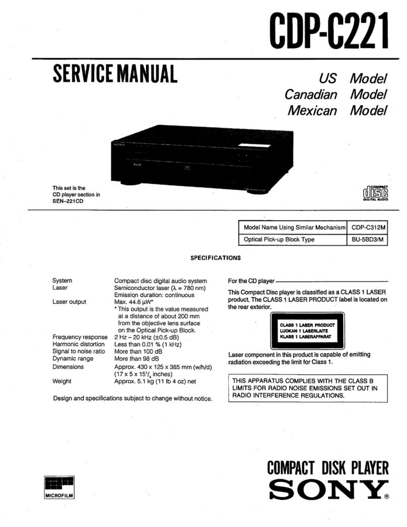
CDP-199/299/491
SERVICE
MANUAL
US
Model
CDP-195/491
Canadian
Model
AEP
Model
E
Model
CDP-
195/295
UK
Model
.
:
CDP-491
‘Australian
Model
CDP-295
Photo
:
CDP-295
Compact
disc
player
Frequency
response
More
than
100
dB
More
than
97
dB
Less
than
0.005%
More
than
95
dB
Signal
to
noise
ratio
Dynamic
range
Harmonic
distortion
Channel
separation
Outputs
LINE
OUT
Output
level
2
V
(at
{phono
jacks)
PHONES
Output
level
max.
1
(stereo
phone
jack)
Load
impedance
over
10
kilohms
Load
impedance
32
ohms
Model
Name
Using
Similar
Mechanism
CD
Mechanism
Type
Optical
Pick-Up
Block
Type
CDP-291/391
CDM14-5BD1
BU-5BD1
SPECIFICATIONS
Supplied
accessories
2Hz-
20
kHz
+
0.5
dB
Audio
cord
1
,
(2
phono
plugs
-
2
phono
plugs)
Remote
commander
(CDP-295/491)
1
R6(size
AA)
batteries
{CDP-295/491}
2
AC
plug
adaptor
(for
some
areas)
:
Remote
commander
RM-D295
(CDP-295/491)
Remote
control
system
50
kilohms)
Infrared
control
Omw
Power
requirements
3
V
DC
with
two
R6
(size
AA)
batteries
Dimensions
Approx.
40
x
20
x
175
mm
(w/h/d)
General
(19/4
"/isX
7
inches)
CDP-195/295/491
Weight
Approx.
95
g
(4
02)
Including
batteries
Power
Model
for
Continental
Europe
requirements
220
~
230
V
AC,
50/60
Hz
Model
for
Canada
120
V
AC,
60
Hz
Model
for
Australia
240
V
AC,
50
Hz
Model
for
other
countries
1140,
120,
220
or
240
V
AC,
50/60
Hz
Design
and
specifications
subject
to
change
without
notice.
This
Compact
Disc
player
is
classified
as
a
CLASS
1
LASER
product.
adjustable,
CLASS
1
LASER
PRODUCT
LUOKAN
1
LASERLAITE
Power
12W
consumption
The
CLASS
1
LASER
PRODUCT
label
is
located
KLASS
1
LASERAPPARAT
Dimensions
430
«
100
»
280
mm
(approx.,
including
(w/h/d)
projections)
(17X4>41'/e
inches)
on
the
rear
exterior.
Weight
(approx.)
3.5
kg
(7
Ibs
12
oz)
COMPACT
DISC
PLAYER
SONY.
CDP-195/295/491
SAFETY-RELATED
COMPONENT
WARNING!!
COMPONENTS
IDENTIFIED
BY
MARK
“AX
OR
DOTTED
LINE
WITH
MARK
AX
ON
THE
SCHEMATIC
DIAGRAMS
AND
IN
THE
PARTS
LIST
ARE
CRITICAL
TO
SAFE
OPERATION.
REPLACE
THESE
COMPONENTS
WITH
SONY
PARTS
WHOSE
PART
NUMBERS
APPEAR
AS
SHOWN
IN
THIS
MANUAL
OR
IN|
SUPPLEMENTS
PUBLISHED
BY
SONY.
ATTENTION
AU
COMPOSANT
AYANT
RAPPORT
A
LA
SECURITE!
LES
COMPOSANTS
IDENTIFIES
PAR
UNE
MARQUE
A
SUR
LES
DIAGRAMMES
SCHEMATIQUES
ET
LA
LISTE
DES
PIECES
SONT
CRITIQUES
POUR
LA
SECURITE
DE
FONC-
TiIONNEMENT.
NE
REMPLACER
CES
COMPOSANTS
QUE
PAR
DES
PIECES
SONY DONT
LES
NUMEROS
SONT
DONNES
DANS
CE
MANUEL
OU
DANS
LES
SUPPLEMENTS
PUBLIES
PAR
SONY.
PROTECTION
OF
EYES
FROM
LASER
BEAM
DURING
SERVICING
This
set
employs
a
laser.
Therefore,
be
sure
to
follow
carefully
the
instructions
below
when
servicing.
CAUTION
Use
of
controls
or
adjustments
or
performance
of
procedures
other
than
those
specified
herein
may
result
in
hazardous
radiation
exposure.
NOTES
ON
HANDLING
THE
OPTICAL
PICK-UP
BLOCK
OR
BASE
UNIT
The
laser
diode
in
the
optical
pick-up
block
may
suffer
electrostatic
breakdown
because
of
the
potential
difference
generated
by
the
charged
electrostatic
load,
etc.
on
clothing
and
the
human
body.
During
repair,
pay
attention
to
electrostatic
breakdown
and
also
use
the
procedure
in
the
printed
matter
which
is
included
in
the
repair
parts.
The
flexible
board
is
easily
damaged
and
should
be
handled
with
care.
1.
Laser
Diode
Properties
*
Material:
GaAiAs
*
Wavelength:
780nm
¢
Emission
Duration:
continuous
*
Laser
Output:
max.44.6uW*
*
This
output
is
the
value
measured
at
a
distance
of
about
200mm
from
the
objective
lens
surface
on
the
Optical
Pick-up
Block.
2.
During
service,
do
not
take
the
Optical
Pick-up
Block
apart,
and
do
not
adjust
the
APC
circuit.
If
there
is
a
breakdown
in
the
APC
circuit
(including
laser
diode),
replace
the
entire
Optical
Pick-
up
Block
(including
APC
borad).
TABLE
OF
CONTENTS
Section
Title
Page
Section
Title
Page
Whee
SGENERAL
vecccecceteicsececnsnntei
dace
seniue
catestinacss
4
4-2.
Block
Diagrarm
oo...
eseesteseenesseaeesenees
10
Location
of
Controls
..........cccccsccssseeeesteesessteseceseneerees
4
4-3.
WaAVETOIMS
.....ceeeeecccteesessessentesenscnstavsesecsseeeseatens
13
4-4.
Printing
Wiring
Boards
..........cccsesesesereeseeees
14
2.
ELECTRICAL
BLOCK
CHECKING
...............
5
4-5.
Schematic
GiaQram
.........eceeececeeseeesesseeeneeees
17
4-6.
Semiconductor
Lead
Layouts
«0.0...
eee
21
4-7.
IC
Block
Diagrams
oo...
ceseseesseeeesesaeseeens
22
3.
DISASSEMBLY
OF
BASE
UNIT...................:
7
5.
EXPLODED
VIEWS.
........cc:scsccetcsseetnssecssneneenes
24
4)
DIAGRAMS
wiiciectevceccsnsstonctacncneAcruecstacsceneets
8
i
Sener
rn
ete
eee
:
6.
ELECTRICAL
PARTS
LIST
oecsssssscssssssuneen
28
MODEL
IDENTIFICATION
~
SPECIFICATION
LABEL
-
CDP-195
CDP-295
CDP-491
SONY.
MODEL
NO.
CHUA
LLL
SERIAL
NO.
MADE
IN
JAPAN
US,
Canadian
MODEL:
AC120,
60Hz
12W
AEP
MODEL:
AC220-230V,
50/60Hz
Australian
MODEL:
AC240V,
50/60Hz
E,
Saudi
Arabian
MODEL:
AC110-120,
220-240V,
50/60Hz,
12W
SAFETY
CHECK-OUT
After
correcting
the
original
service
problem,
perform
the
following
safety
check
before
releasing
the
set
to
the
customer:
Check
the
antenna
terminals,
metal
trim,
"metallized"
knobs,
screws,
and
all
other
exposed
metal
parts
for
AC
leakage.
Check
leakage
as
described
below.
LEAKAGE
TEST
The
AC
leakage
from
any
exposed
metal
part
to
earth
ground
and
from
all
exposed
metal
parts
to
any
exposed
metal
part
having
a
return
to
chassis,
must
not
exceed
0.5mA
(500
microampers).
Leakage
current
can
be
measured
by
any
one
of
three
methods.
1.
A
commercial
leakage
tester,
such
as
the
Simpson
229
or
RCA
WT-540A.
Follow
the
manufacturers’
instructions
to
use
these
instruments.
2.
A
battery-operated
AC
milliammeter.
The
Data
Precision
245
digital
multimeter
is
suitable
for
this
job.
CDP-195/295/491
CDP-195
CDP-295
CDP-491
SONY.
MODEL
NO.
LLLLLL
MLL
SERIAL
NO.
MADE
IN
FRANCE
AEP
MODEL:
AC220-230V,
50/60Hz
UK
MODEL:
AC240V,
50/60Hz
3.
Measuring
the
voltage
drop
across
a
resistor
by
means
of
a
VOM
or
battery-operated
AC
voltmeter.
The
"limit"
indica-
tion
is
0.75V,
so
analog
meters
must
have
an
accurate
low-
voltage
scale.
The
Simpson
250
and
Sanwa
SH-63Trd
are
examples
of
a
passive
VOM
that
is
suitable.
Nearly
all
battery
operated
digital
multimeters
that
have
a
2V
AC
range
are
suitable.
(See
Fig.A)
To
Exposed
Metal
Parts
on
Set
{
AC
voltmeter
(0.75
V)
=
Earth
Ground
Fig.
A.
Using
an
AC
voltmeter
to
check
AC
leakage.
CDP-195/295/491
SECTION
1
GENERAL
LOCATION
OF
CONTROLS
This
section
is
extracted
from
instruction
manual.
CDP-295
[1]
POWER
switch
[2]
Disc
tray
Remote
sensor
[41]
Display
window
[5
}
PROGRAM
button
CHECK
(program
check)
button
Numeric
buttons
CLEAR
(program
clear)
button
>12
(over
12)
button
MUSIC
SCAN
button
PEAK
SEARCH
button
PHONE
LEVEL
control
FADER
button
PHONES
jack
REPEAT
button
EDIT/TIME
FADE
button
He-¢
</P>
PPI
(AMS
*/RMS**
/manual
search)
buttons
lf
(stop)
button
18
(pause)
button
>
(play)
button
&
(open/close)
button
Jelke|
+
=e
RBS
Bee
ele
Ele
*
AMS
is
the
abbreviation
of
Automatic
Music
Sensor.
**
RMS
is
the
abbreviation
of
Random
Music
Sensor.
SECTION
2
CDP-195/295/491
ELECTRICAL
BLOCK
CHECKING
Note:
1.
CD
Block
basically
constructed
to
operate
with-
out
adjustment.
Therefore,
check
each
item
in
order
given.
2.
Use
YEDS-18
disc
(3-702-101-01)
unless
otherwise
indicated.
3.
Use
the
oscilloscope
with
more
than
1OMQ
im-
pedance.
4.
Clean
an
object
lens
by
an
applicator
with
neutral
detergent
when
the
signal
level
is
low
than
specified
value
with
the
following
checks.
S
Curve
Check
oscilloscope
BD
board
rene,
TP
(FEO)
o~w——o}
TP(VC)
ow—lo-
Procedure
:
1.
Connect
oscilloscope
to
test
point
TP
(FEO)
on
BD
board.
2.
Connect
between
test
point
TP
(FES)
and
TP
(VC)
by
lead
wire.
3.
Turned
Power
switch
on
and
actuate
the
focus
serch.
(actuate
the
focus
serch
when
disc
table
is
moving
in
and
out.)
4.
Check
the
oscilloscope
waveform
(S
curve)
is
symmetrical
between
A
and
B.
And
confirm
peak
to
peak
level
within
341Vp-p.
S
curve
waveform
symmetry
within
3+1Vp-p
5.
After
check,
remove
the
lead
wire
connected
in
step
2.
Note:
*
Try
to
mesure
several
times
to
make
sure
that
the
ratio
of
A:
B
or
B:
A
is
more
than
10:7.
»
Take
sweep
time
as
long
as
possible
and
light
up
the
brightness
to
obtain
best
waveform.
RF
Level
Check
oscilloscope
TP
(RFO)
OO
TP
(VC)
sea
(ek
Procedure
:
1.
Connect
oscilloscope
to
test
point
TP
(RFO)
on
BD
board.
2.
Turn
Power
switch
on.
3.
Put
disc
(YEDS-18)
in
and
playback.
4.
Confirm
that
oscilloscope
waveform
is
clear
and
check
RF
signal
level
is
correct
or
not.
Note:
Clear
RF
signal
waveform
means
that
the
shape
“©”
can
be
clearly
distinguished
at
the
center
of
the
wave-
form.
VOLT/DIV
:
200mv
TIME/DIV
:
$00nS
WR
WY
le
401000000004
$02)
COHAN
|
228%
vee
RF
signal
waveform
\)
909,
\N
AKA)
(WY
7,9
A)
Wy
NA
E-F
Balance
Check
oscilloscope
BD
board
—)
TP
(TEO)
ot
—0F
TP
(VC)
O=—0-
Procedure
:
1.
Connect
test
point
TP
(ADJ)
to
ground
and
TP
(TES)
to
TP
(VC)
with
lead
wire.
2.
Connect
oscilloscope
to
test
point
TP
(TEO)
on
BD
board.
Turn
Power
switch
on.
Put
disc
(YEDS-18)
in
and
playback.
Confirm
that
the
osilloscope
waveform
is
sym-
metrical
on
the
top
and
bottom
in
relation
to
OV,
and
check
this
level.
symmetry
level
:
21Vp-p
Traverse
oscilloscope
ANY
Uh
ov
HA
tial
6.
Remove
the
lead
wire
connected
in
step
1.
le
D2
99)
2999/69"
RF
PLL
Free-run
Frequency
Check
{
BD
BOARD
|]
-
Component
Side
-
Procedure
:
1.
Connect
frequency
counter
to
test
point
(PLCK)
with
lead
wire.
f
t
Main
board
requency
counter
ita
oe
TP
(PLCK)
oe
Turn
Power
switch
on.
Confirm
that
reading
on
frequency
counter
is
4,
3218MHz.
Focus/Tracking
Gain
This
gain
has
a
margin,
so
even
if
it
is
slightly
off.
There
is
no
problem.
Therefore,
do
not
perform,
this
adjustment.
Please
note
that
it
should
be
fixed
to
mechanical
cen-
ter
position
when
you
moved
and
do
not
know
original
position.
Adjustment
Location
;
{MAIN
BOARD]
-
Component
Side
—
1C301
(
conductor
side
)
1€302
TP
|
(
PLCK
)
SECTION
3
DISASSEMBLY
Note:
Follow
the
disassembly
procedure
in
the
nomerical
order
given.
@
Turn
the
cam
to
the
direction
of
arrow
(Counter
clock
wise)
by
minus
screw
driver.
Take
off
the
disc
table.
Remove
the
yoke
bracket.
Remove
the
MD
(BU-5BD1)
to
the
direction
of
arrow.
oR)
CDP-195/295/491
4)
CDP-195/295/491
4-1.
SECTION
4
DIAGRAMS
PIN
FUNCTION
OF
1C101
AND
IC401
@iCi01
(CXA1372Q)
PIN
FUNCTION
Prine
|
eneme
[1/6
[pion
GND
when
two
(+)
dual
power
supplies
are
in
use,
or
the
center
voltage
(2.5V)
when
a
single
power
supply
is
in
use.
Time
constants
for
gain
switching
in
normal
mode/down
mode
and
for
focus
gain
are
conncted
between
the
FGD
and
FS3
pins.
The
capacitor
for
low
frequency
boost
in
the
focus
servo
loop
is
connected.
Focus
drive
output.
Inverted
input
to
focus
amplifier.
Time
constants
to
generate
the
focus
search
waveform
are
connected.
Time
constants
for
gain
switching
in
normal
mode/up
mode
and
for
tracking
gain
are
wolalNa
A)
a
[wl
ve
me
ee
et
connected
between
TGU
pin
and
TG2
pin.
=
Q
AVCC
|
Analog
power
supply
(5V
when
+
dual
power
supplies
are
in
use,
5V
when
a
single
power
supply
is
in
use.)
ett
oe
tN
Tracking
drive
output.
Inverted
input
to
tracking
amplifier.
Non-inverted
input
to
sled
amplifier.
Sled
drive
output.
Non-inverted
input
to
sled
amplifier.
or
ad
Oo
on
OD
tS
Qo
ESET
ISET
AVEE
The
610k
phase
compensator
resistor
is
connected
to
this
pin.
The
current
setting
resistor
is
connected
to
this
pin.
a
le
Oe
O
The
limit
switch
is
connected
to
this
pin.
Analog
power
supply
(—5V
when
+
dual
power
supplies
are
in
use,
or
GND
when
a
single
power
supply
is
in
use.)
Direct
control
pin.
NR
NN
me
WN
CLK
Sled
run-away
prevention
circuit
operates
when
this
signal
is
”L”.
Serial
data
transfer
clock
input
that
is
supplied
from
CPU
(or
DSP).
Latch
input
from
CPU
(or
DSP).
Serial
data
input
from
CPU
(or
DSP).
System
reset.
”L”
to
reset.
25
XRST
26
C.OUT
27
SENS
28
DGND
=
Output
to
tracking
counter.
SENS
output.
Digital
ground
(GND).
(GND
when
+
single
power
supply
is
in
use.)
0
Oln
sR
me
Ie
dual
power
supplies
are
in
use.
GND
when
a
Mirror
output.
Defect
output.
"H”
when
defective.
29
|
MIRR
30
_|
DFCT
31‘
|
ASY
32
|
EFM
33.
|
FOK
34
CC2
35
__|
col
Auto-assymmetry
control
input.
EFM
comparator
output.
Focus
OK.
Defect-bottom-hold
input
(inout
by
capacitive
coupling).
Defect-bottom-hold
output.
w
for)
Ba
ww
Ww
oo
fos
CB
cP
RF1
RFO
Digital
power
supply.
(+5V
when
+
dual
power
supplies
in
use.
+5V
when
a
single
power
supply
is
in
use.)
The
defect-bottom-hold
capacitor
is
connrcted
to
this
pin.
The
mirror
hold
capacitor
is
connected
to
this
pin.
RF
signal
input
(input
by
capacitive
coupling).
RF
signal
input
(input
by
DC
coupling).
»
mn
—|—
Digital
power
supply
(—5V
when
+
dual
power
supplies
are
in
use.
GND
when
a
single
power
supply
is
in
use.)
—
e-)
42
TZC
Tracking
zero-cross
comparator
input.
43
TE
Tracking
error
input.
44
TDFCT
The
defect
prevention
hold
capacitor
is
connected
to
this
pin.
45
|
ATSC
Anti-shock
input.
46
Focus
zero-cross
comparator
input.
47
Focus
error
input.
The
defect
prevention
hold
capactior
is
connected
to
this
pin.
CDP-195/295/421
©
{C401
(CXP50112-697Q)
PIN
FUNCTION
Description
Not
used
(open).
Common
output
to
FL
tube.
Muting
on
by
"H”,
Muting
off
by
”L”.
55-58
|
BO-
B3
—~
|
Not
used
(+5V)
Segment
output
to
FL
tube.
;
29
Subcode
sync
signal
SO
+
S1
detection
input
from
IC301
(CXD2500AQ).
30
Not
used
(open).
31
+5V
:
32
Reset
input.
33
+5V
34
Power
voltage
terminal
(+5V).
35-40
|
KEYO-
KEY5
I
|
Key
A/D
input.
41
=
—
|Not
used
(Ground).
7
42
TIMER
SW
1
|
Auto
play
select
input
(Auto
play
"L”).
43
=
—
{Not
used
(Ground).
44
CLK
O
|
Serial
data
transfer
clock
output
to
IC301
(CXD2500AQ).
45
DATA
QO
[Serial
data
output
to
1C301
(CXD2500AQ).
46
=
~
|
Not
used
(Ground).
pe
47
FOK
I
|
Focus
OK
signal
input
from
IC101
(CXA1372Q).
48
GFS
I
|
Frame
sync
signal
clock
status
input
from
IC301
(CXD2500AQ).
49
SUBQ
I
|
Sub
code
(Q
data)
serial
input
from
IC301
(CXD2500AQ).
50
SQCLK
QO
|
Sub
code
(Q
data)
readout
clock
output
to
IC301
(CXD2500AQ).
51
XLT
O
|
Serial
data
latch
output.
a
52
PRGL
O
|
Attenuate
data
latch
clock
output
to
1C302
(CXD2554P).
53
LDON
O
|
Laser diode
ON/OFF
select
output
of
optical
pick-up.
54
AMUT
O
|
Muting
output
for
IC301
(CXD2500AQ)
and
Q344
(2SC3399).
59
DEFECT
SW
O
|
Deffect
circuit
ON/OFF
select
output
to
IC101
(CXA1372Q).
60
- —
|
Not
used
(open).
61
SENSE
I
|
SENS
signal
input
from
IC301
(CXD2500AQ).
-
62
RMC
I
|
Remote
control
signal
input.
63
INSW
I
!
Input
for
loading
out
switch.
64
OUTSW
I
|
Output
for
loading
in
switch.
ADJ
I
|
Tset
mode
input.
GFS
check
will
not
activate
by
”L”.
AFADJ
I
|
Test
mode
input.
All
test
operation
will
be
activate
by
"L”
mode
when
power
ay
LODIN
O
|
Output
for
turn
the
loading
motor
to
loading.
LODOUT
O
|
Output
for
turn
the
loading
motor
to
un
loading.
Not
used
(open).
Not
used
(open).
Ground.
Clock
output.
+5V
Clock
input.
(4MHz)
+5V
Power
voltage
—30V
for
built
in
FL
tube
controller.
Not
used
(open).
Not
used
(open).
Not
used
(open).
Not
used
(open).
4-6.
SEMICONDUCTOR
LEAD
LAYOUTS
CXA13720
(TOP
ViEW)
GP1U52XB
RD5.6ES-B2
RD6.8ES-B1
RD7.5JS-B2
ISS202-1
11ES2
11EQS04
[em
catnede
anode
i
u
2SD774-34
CXD2500AQ
CXP50112-0970
IN4148M
r
anode
2SA1175-HFE
-?1-
CXD25520
'24345
2SB1094-L
2SB1274SA-RS
CD9-795/2.95/497
DTA1.4ES
DT014
4ES
23C02483-YGR
2E
C262
3A-LK
2D4.7M-B1
o>
we
wa
age
rd
|
{k
\
2SC1815-Y
4-7.
IC
BLOCK
DIAGRAMS
1¢101
CXA13720
3
-
os
“
=
>
SE
g
26
&
S
a8
5
rd
&
ge
Fo
a
$8
@
a
o
8
2
rr
2
aS
ra
a 3
&
G)}—
BHD)
(32)
(i)
—GS)—
oe
(s)
cow
ara]
OMFAAATOR}
BUEFER
DATA
eB
4?
¥W
re
XLT
cP
oF
RFA
4
|
re)
clk
neo
ne
me
Lock
(20)
DIRC
(19)
AVEE
DVEE
(41)
TZC
y
y
y
y
[cowPaRATOR}
(1s)
ssToP
@
i
FS1-4
[email protected]
TMI-7
PSI-3
b
Tal
Te
@)
DFCT
T.GAIN
[
3
ae
o
UP/DOWN
TRACE
ING
[1°
set
}@2)
Iset
ToFCT
(Ke
Pv
by,
hg
CoureN:
(18)
FSET
ase
©
ee
acd
aeee
re
6
FSI
é
SERVO
Fz
@)
F
Seance
bo
OS)
tug
ONZCHOP
©
:
eGKIN
pens
©)
“ON
ie
Oa
FE
(@”)
DFCT
_DOWN/NORMAL
Ea
o%
ae
Lo
Q
oe
o
W7
SLED
Ses
eer]
|
HOT
oe
Forct
@)
ess
\)
if
§
‘
192
FOCUS
ES?)
1.
GAIN
(13)
sL+
ON/OFF
>
eee
UP/DOWN
5
Tuz
ir
TRACK
|
NG|
\
SLED
e
Po
LAMP
ON/OFF
8
!
OO
CH)
EHO)
0)
S 8
a2
3
og
ow
B36
8
2
o«
2
2
@
Bog
gees
ec
&
z
10103
M54641L
et
|
REFERENCE
oe
(2)
OUT
2
1C201
M5293L
AMP.
-_
(7)
ouT
1
GND
REFERENCE
VOL
TAGE
REFERENCE
VOLTAGE
(3)
our
OVERCURRENT
LIMITTER
1c302
CXD2554P
1C202
M5290P-16
ATTENATOR
(9B)
COUNTERD
PARALLEL
~
SERIAL
CONVERTER
US
TH-
ORDER
FIA
CALCULATION
aoM
BUFFER
RaW
Ram
FOR
ue
FIR
NOISE
SHAPER
&
ANUTHMETIC
CIRCUIT
ROUND
OFF)
a
SBS0
IC305
CXD2552AQ
SCOR
FSW
WFCK
EMP
MON
“
By
yn
a
»
©
f
a
MBP
Bo ie
a
eee
rai
g
mos
agi
tar
|
“Gd
80uT
6)
®
6)
LOCK
OUT
(59)
MB2
NC
vss
VARI
ABLE
128FS
vcoo
Bea
C16M
Lo
@)
ae
vcol
CONTROL
C4M
vpD
TiMING
CIRCUIT
SYNC
VSUB
TEST2
Loe
g
vss
TESTI
ae
a
FSTT
XTSL
XIN
GB)
vss
=
XTAQ
xouT
i—|
ue
:
ATA
xvpb
THIRD
ORDER
NC
ae
PLM
|
NOISE
SHAPER
—1
=
BCKi
NC
vss
a
||
se
[$9
APTL
vss
(i)
VCK1
MUTE
APTR
e
TEST3
FILO
on
FILI
SAO?
O_O)
@)
(@)}——()
PCO
aw
T
a
Nn
i<] i=]
N
anh
t Q
BANS
efe
S
8B
Soa
a
® §
AVSS
=
eg
¢
&
3
CLTV
BA04
a
ADDRESS
Qa05
AVaD
GENERA-
BADE
DA07
RF
QA08
"A
DATA
PROCESSOR
DA09
amo
ee
ied
load
N-
oO
rics
Q
wnyMATS
io
<td
>
a
ta
atatata
FA
a
‘
AMAAAAGE
-~23-
CDP-195/295/491
NOTE:
+
~-XX,
-X
mean
standardized
parts,
so
they
may
have
some
differences
from
the
original
one.
The
construction
parts
of
an
assembled
part
are
indicated
with
a
collation
number
in
the
rernark
column.
Color
indication
of
Appearance
Parts
Example:
KNOB,BALANCE(WHITE)...(RED)
T
Parts
color
Cabinet's
color
(1)
CABINET
SECTION
2
not
supplied
Canadian
MODEL
~
EXCEPT
US,
——
E>
SECTION
5
EXPLODED
VIEW
Items
marked
“*”
are
not
stocked
since
they
are
seldom
required
for
routine
service.
Some
de-
lay
should
be
anticipated
when
ordering
these
items.
*
The
mechanical
parts
with
no
reference
num-
ber
in
the
exploded
views
are
not
supplied.
Hardware(#
mark)
list
is
given
in
the
last
of
this
parts
list.
The
components
identified
by
mark
A
or
dotted
line
with
mark
A\
are
critical
for
safety.
Replace
only
with
part
number
specified.
Les
composants
identifiés
par
une
marque
A\
sont
critiques
pour
la
sécurité.
Ne
les
remplacer
que
par
une
piéce
por-
tant
le
numéro
spécifié.
supplied
with
J501
'
AEP
MODEL!
E
MODEL
|
MODEL
‘US,
Canadian
1
not
supplied
11)
CABINET
SECTION
|
!
|
ay
SS
|
cas
!
Jie
2,2
|
PD
oO
pe
ON
LAE
tS
SR
a
EID
i
|
Australian
'US,
Canadian
|
+;
MODEL
4.
|MODEL
i
ENS
|
|
!
|
a
few
[not
supplied
not
supplied
~
not
supplied
lin,
not
supplied
=
#1
#1
EXCEPT
US,
——!
FLD401
supplied
with
RV501
Canadian
MODEL
supplied
with
J501
oo
—
MD
SECTION
(CDM14-5BD1)
(2)
(including
315)
PICK-UP
BLOCK
(BU-5BD1)
(3)
oO
uy)
oO
M102
(including
ml

This manual suits for next models

2

Other Sony CD Player manuals

Sony Walkman D-NE511 User manual

Sony

Sony Walkman D-NE511 User manual

Sony Walkman D-SJ17CK User manual

Sony

Sony Walkman D-SJ17CK User manual

Sony CDX-705 - Compact Disc Changer System User manual

Sony

Sony CDX-705 - Compact Disc Changer System User manual

Sony MZ-N510CK User manual

Sony

Sony MZ-N510CK User manual

Sony DVP-NC85H - HDMI/CD Progressive Scan DVD... User manual

Sony

Sony DVP-NC85H - HDMI/CD Progressive Scan DVD... User manual

Sony CD Walkman D-FJ200 User manual

Sony

Sony CD Walkman D-FJ200 User manual

Sony D-NF611 - Portable Cd Player User manual

Sony

Sony D-NF611 - Portable Cd Player User manual

Sony D-FJ210 - CD Walkman Player User manual

Sony

Sony D-FJ210 - CD Walkman Player User manual

Sony DVP-FX980 User manual

Sony

Sony DVP-FX980 User manual

Sony XP-EV500 User manual

Sony

Sony XP-EV500 User manual

Sony RM-X60M - Marine Remote Commander User manual

Sony

Sony RM-X60M - Marine Remote Commander User manual

Sony CDX-605 - Compact Disc Changer User manual

Sony

Sony CDX-605 - Compact Disc Changer User manual

Sony CFD-RG880CP User manual

Sony

Sony CFD-RG880CP User manual

Sony CDX-605 - Compact Disc Changer User manual

Sony

Sony CDX-605 - Compact Disc Changer User manual

Sony MZ-N10 User manual

Sony

Sony MZ-N10 User manual

Sony CDP-C450Z User manual

Sony

Sony CDP-C450Z User manual

Sony Walkman D-EJ101CK User manual

Sony

Sony Walkman D-EJ101CK User manual

Sony CDP-CA70ES - Compact Disc Player User manual

Sony

Sony CDP-CA70ES - Compact Disc Player User manual

Sony MDX-65 User manual

Sony

Sony MDX-65 User manual

Sony SCD-XA9000ES - Es Super Audio Cd Player User manual

Sony

Sony SCD-XA9000ES - Es Super Audio Cd Player User manual

Sony CFD-C646 User manual

Sony

Sony CFD-C646 User manual

Sony D-FJ61 D-FJ65 User manual

Sony

Sony D-FJ61 D-FJ65 User manual

Sony Walkman D-EJ775 User manual

Sony

Sony Walkman D-EJ775 User manual

Sony SCD-XE600 User manual

Sony

Sony SCD-XE600 User manual

Popular CD Player manuals by other brands

Hamilton/Buhl Mark 4 Opus user manual

Hamilton/Buhl

Hamilton/Buhl Mark 4 Opus user manual

Micromega CD-10 operating manual

Micromega

Micromega CD-10 operating manual

MC Crypt CMP-920 instruction manual

MC Crypt

MC Crypt CMP-920 instruction manual

IMG STAGE LINE CD-290DJ instruction manual

IMG STAGE LINE

IMG STAGE LINE CD-290DJ instruction manual

Resolution Opus 21 owner's manual

Resolution

Resolution Opus 21 owner's manual

Pioneer PD-65 operating instructions

Pioneer

Pioneer PD-65 operating instructions

Philips AZ700T/37 user manual

Philips

Philips AZ700T/37 user manual

Panasonic SLSX270 - PORT. CD PLAYER operating instructions

Panasonic

Panasonic SLSX270 - PORT. CD PLAYER operating instructions

Philips AZ7265/17 Instructions for use

Philips

Philips AZ7265/17 Instructions for use

Muse M-29 RD user manual

Muse

Muse M-29 RD user manual

Gogen PDXD 962 DVBT user manual

Gogen

Gogen PDXD 962 DVBT user manual

Pioneer CDJ-500II operating instructions

Pioneer

Pioneer CDJ-500II operating instructions

Philips CDR600/00/17 Service manual

Philips

Philips CDR600/00/17 Service manual

TRETTITRE T-CP8 manual

TRETTITRE

TRETTITRE T-CP8 manual

Kenwood CD-323M instruction manual

Kenwood

Kenwood CD-323M instruction manual

Fisher Fisher SLIM-1800 Service manual

Fisher

Fisher Fisher SLIM-1800 Service manual

JVC RC-EZ35S instructions

JVC

JVC RC-EZ35S instructions

Magnavox AZ1100 - Single Deck user manual

Magnavox

Magnavox AZ1100 - Single Deck user manual

manuals.online logo
manuals.online logoBrands
  • About & Mission
  • Contact us
  • Privacy Policy
  • Terms and Conditions

Copyright 2025 Manuals.Online. All Rights Reserved.