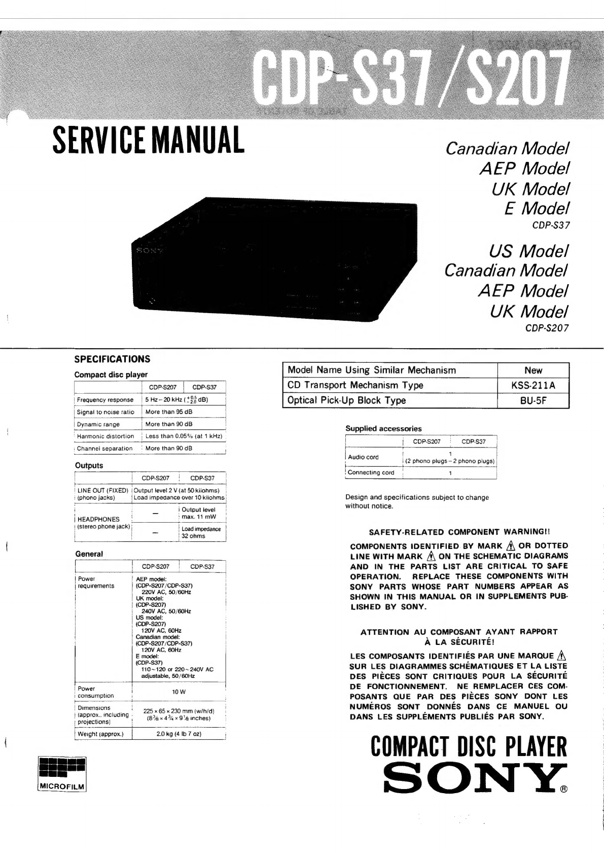
Sony CDP-S37 User manual
Other Sony CD Player manuals

Sony
Sony D-E200 Primary User manual

Sony
Sony Walkman D-NE301SR User manual

Sony
Sony Hi-MD Walkman MZ-RH10 User manual

Sony
Sony CDX-505RF - Compact Disc Changer System User manual

Sony
Sony DVP-FX730 - Portable Dvd Player User manual

Sony
Sony CDP-C321 User manual

Sony
Sony CDX-GT615UV User manual

Sony
Sony MZ-R500 User manual

Sony
Sony PDW-F30 User manual

Sony
Sony CDX-G1152U User manual

Sony
Sony CFD-V25 - Cd Radio Cassette-corder User manual

Sony
Sony XDCAM PDW-1500 User manual

Sony
Sony CD Walkman D-EJ855 User manual

Sony
Sony CDP-CE415 User manual

Sony
Sony CDP-XE200 User manual

Sony
Sony Walkman D-NF610 User manual

Sony
Sony CDX-MP30 User manual

Sony
Sony CD Walkman D-EJ011 User manual

Sony
Sony CD Walkman D-ES52CK User manual

Sony
Sony MZ-B100 - Minidisc Business Product Recorder User manual