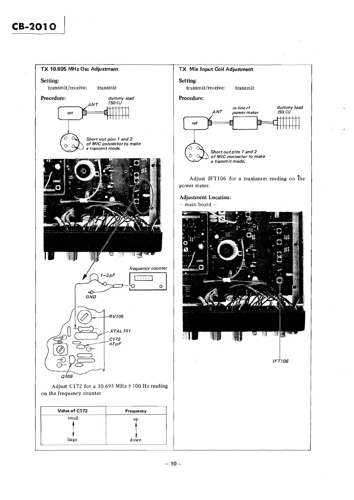
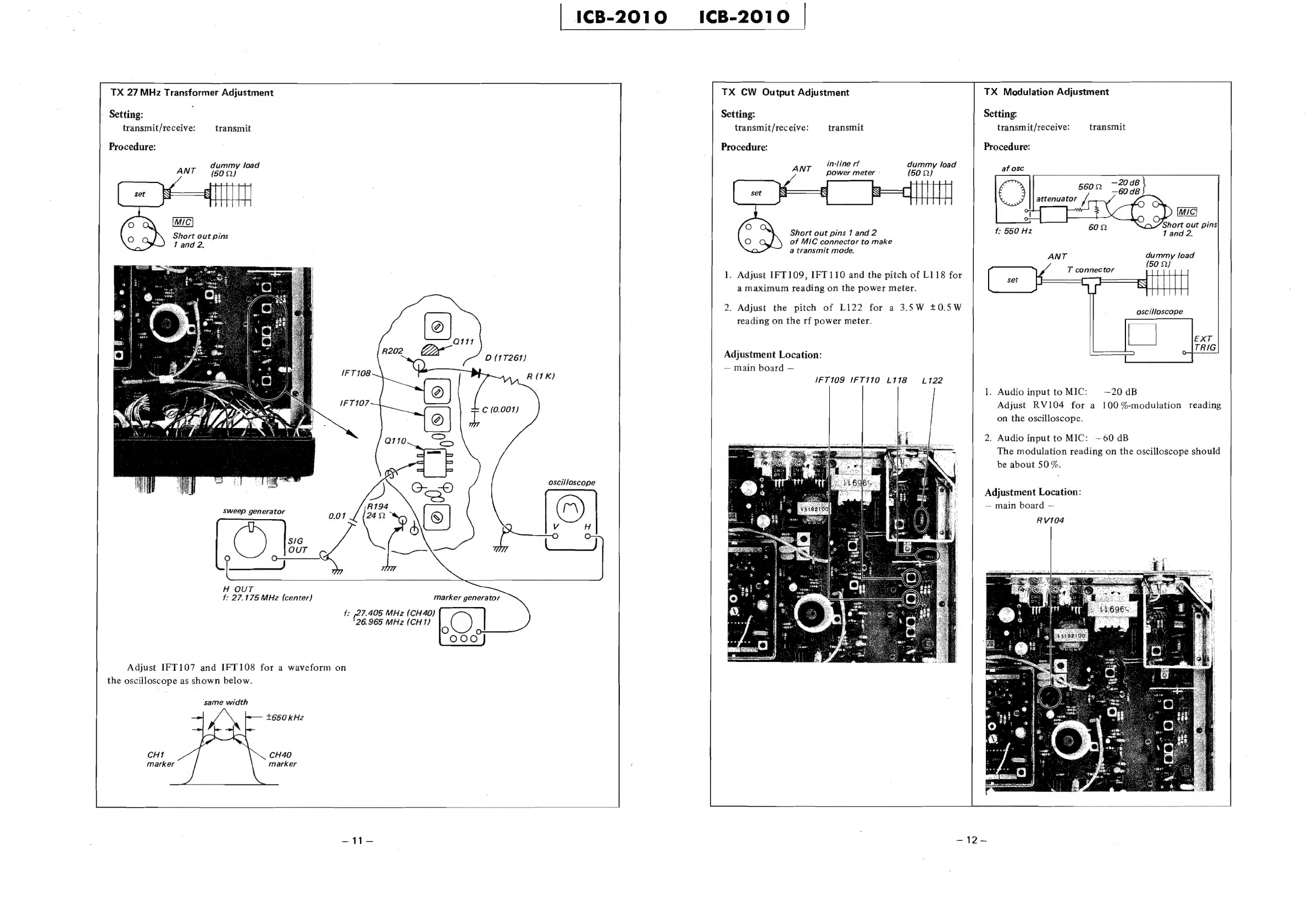
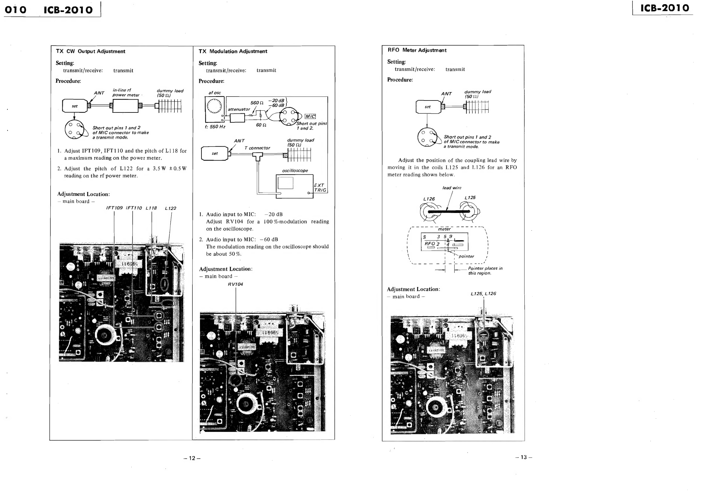
Sony ICB-2010 User manual

US
Model
GENERAL
Operating
Frequency:
Antenna:
Communication
System:
Power
Requirement:
Dimensions:
Weight:
TRANSMITTING
SECTION
Transmitting
Power:
Frequency
Tolerance:
Circuitry:
SPECIFICATIONS
Within
the
26.965
—
27.405
MHz
band
40
channels
full
coverage
(on
page
26)
External
Antenna
Connector
coaxia!
connector
type
SO-239
Push-to-talk
system
13.8
V
de
(from
positive
or
negative
grounded
12
V
car
battery)
209
(w)
x
64
(h)
x
256
(d)
mm
8Y4
(w)
x
2%
(h)
x
10%
(d)
inches
including
projecting
parts
and
controls
2.1
kg,
41b
10
oz
4w
+0.005
%
(—30°C
to
+60°C)
P.L.L.
synthesizer
with
quartz
crystal
controlled
circuit
a
ff
Hogs
©
Modulation:
Current
Drain:
Spurious
Response:
RECEIVING
SECTION
Circuitry:
Maximum
Sensitivity:
Selectivity:
Intermediate
Frequency:
Audio
Power
Output:
Current
Drain:
Speaker:
Collector
modulation
in
final
and
driver
stage
1
A
without
modulation
More
than
60
dB
P.L.L.
synthesizer
with
quartz
crystal
controlled
circuit
Dual
conversion
superheterodyne
Less
than
0.6
nV,
at
S/N
=
6dB
—60
dB
at
10kHz
10.695
MHz
455
kHz
Ist:
2nd:
1.5
W
(AM)
at
10
%
distortion
4.0
W
(PA)
270
mA
at
zero
signal
9.2
cm
(348
inches)
dia.
8
ohms

CB-2010
SECTION
1
OUTLINE
BLOCK
DIAGRAM
1-1.
0102
-
831
AlddNS
YSMOd
———H—_..
XL
(A6)
ate
b-2S
p-25——
+9
:
,
re
Yd
iV
[
Ci
XL
HNG96'9Z
HIN
6201
221210
,
ner
hase
veld
yal
WHO
Os
ZHNS69‘0
i
ABEL
IA
@
[wamog]
dhs
Nand
xy
vito
9s
WNid
XL]
|
yaaa
XL
var'e
FzI0
asng
ONIHOLIMS
1a
Madfi§
YaMOd
re
~NOLLYTINGOW
—
HOLIMS
T3NNWHO
de
ZHWb2
‘0!
a
e
aired
as
(MBIA
Wv3e)
10EX
ZH
HOI
|
[£91
8OE-10E0
:
dV
IK
UAZISSHINAS
Tid
aS
1X3
er
]
o—!
iy
ZHWI2'91
lg
22I-6110
38
ZHNL2'9I
Md
dV
HO7aNOS]
o
diy
av
EOIAY
2-2§
3
4d]
vd
ZL
LNd.LNO/NOILYINGOW
a
P
aanoe
[Wa]
te
iOlAd
;
gor'soi0
£0I0
3WMTIOA
3
iz
U
yin
dW
3!
XIW
ISI
ors
————
NOILW1ndow
‘3¥
—
sia
zaln
WI)
ZH¥
OCD
ZHNS69'0|
ZHWSOb'LZ
ae
0}
“Om
11S
ZHWG96
92
xa
XY
ONILLINSNYAL
+
XL
ONIAIZO3Y
:
XY

|
ICB-2010
ICB-2010
|
SYNTHESIZER
BLOCK
REMOVAL
shield
case
A
cover
SECTION
2
DISASSEMBLY
CASE
REMOVAL
Top
Case:
°
@
Bottom
0
3)
:
@
@
835
(black)
Note:
The
synthesizer.
board
can
be
repaired.
How-
ever,
the
conductor
side
of
the
board
is
not
accesible
during
a
check
because
of
the
shield
case
A.
top
case
synthesizer
circuit
board
(black)
(black)
shield
case
A
|
4
PS3x6
(through
circuit
board)
SPEAKER
REMOVAL
Remove
the
speaker
from
the
speaker
holder.
bottom
case
8
(black)
©
83x
5
(black)
SWITCH
BOARD,
LED
BOARD
and
METER
REMOVAL
ae
Note:
channel
indicator
:
f
LED
holder
When
reattaching
the
LED
circuit
board,
do
not
let
the
portion
shown
with
*
touch
the
click
mechanism
of
the
channel
selector.
LED
circuit
FRONT
PANEL
REMOVAL
LOWER
CUSHION
REMOVAL
switch
circuit
board
Note:
Do
not
remove
the
lower
cushion
completely
except
when
a
lower
cushion
replacement
is
required.
Note:
The
front
panel
has
MIC
connector
mounted
on
it,
and
the
front
panel
can
be
removed
forward
about
10
cm
(4
inches).
chassis
front
panel
lower
cushion
8
B3x5
(black)
switch
knob
channel
selector
TX
indication
LED
(black)
C1)
Pull
off
four
knobs.
@
B
3x
6
(black)

ICB-2010
ICB-2010
SECTION
3
ADJUSTMENTS
Setting:
Unless
otherwise
specified,
set
the
switches
and
controls
as
follows.
4.
The
coaxial
cables
used
for
connecting
the
ANT
connector
and
the
rf
power
meter,
and
the
rf
power
meter
to
the
dummy
load
are
to
be
as
short
as
possible.
If
the
cables
are
long,
SWR
indication
Synthesizer
10.24
MHz
Adjustment
Procedure:
Adjustment
Location:
—
synthesizer
board
—
C322
POWER
site
oN
differs
from
the
true
value
due
to
the
cable
Channel
selector:
18
loss.
EMERGENCY
CH
switch:
OFF
CB/PA
switch:
CB
5.
It
is
preferable
to
use
a
low-capacitive
probe
with
DX/LOCAL
switch:
DX
the
frequency
counter
not
to
interrupt
the
circuit
RFO/SWR
switch:
RFO
connected.
If
such
a
probe
is
not
available,
VOLUME
control:
maximum
precisely
follow
the
procedure
in
this
manual.
SQUELCH
control:
fully
counterclockwise
Transmit/receive:
receive
Power
supply
voltage:
.
13.8
V
de
Test
Equipment
Required:
@®
Rf
signal
generator
(AM)
Regulated
dc
power
supply
(13.8
V,
3
A)
®
Rf
dummy
load
(non-inductive
502,
more
than
10W)
®@
Oscilloscope
(30MHz,
with
triggered
CH1
only
provision)
@
Sweep
generator
(30
MHz)
IFT303
@
In-line
rf
power/SWR
meter
(502,
more
than
a>
10
W,
up
to
50
MHz)
.
@
Frequency
counter
(30
MHz,
sensitivity
50
mV)
ae
@
Audio
signal
generator
(with
attenuator
down
to
60
dB)
@
Audio
millivoltmeter
®
Coaxial
cable
assemblies
(50
Q2,
less
than
one
foot,
fitted
with
plugs)
GND
frequency
counter
1-2
pF
°
Note
on
Adjustment
1.
TX
means
transmitter
RX
means
receiver
GND
oscilloscope
2.
Unless
otherwise
specified,
input
levels
are
to
be
as
low
as
possible
for
the
adjustments.
probe
3.
The
maximum
current
drain
in
transmitting
is
ae
about
1A.
A
regulated
dc
power
supply
of
1A
is
insufficient.
Use
a
power
supply
of
2A
or
more.
GND
1.
Adjust
C322
for
a
10.24MHz
+
100
Hz
reading
on
the
frequency
counter.
Value
of
C322
Frequency
small
up
large
down
2.
Adjust
IFT303
for
a
maximum
reading
on
the
oscilloscope.

iCB-201¢
Synthesizer
Tripler
Adjustment
Procedure:
‘e=
Q304
R320
is
680
(=)
Ground
the
lead
of
R320.
oscilloscope
[_]
Adjust
IFT304
for
a
maximum
waveform
reading
(15.36
MHz)
on
the
oscilloscope.
Adjustment
Location:
~—
synthesizer
board
—
1FT304
Synthesizer
VCO
Adjustment
Procedure:
C318
VOM
S|]
[A]
+
oO
}.
Channei
selector:
1
Adjust
L301!
using
a
plastic
hexagonal
screwdriver
fora
1
Vdc
reading
on
the
VOM.
2.
Change
the
channel
selector
from
|
through
40.
VOM
reading
should
gradually
change
from
|
V
(channel
|)
to
3.4
V
(channel
40).
Adjustment
Location:
--
synthesizer
board
—
L307

-B-2010
5
:
Synthesizer
PLL
Output
Adjustment
RX
Ant,
Rf
and
1st
1F
Adjustment
Procedure:
Procedure:
.
R332
2002
output
AM
rf
signal
generator
.
oscilloscope
30
%
amplitude
modulation
by
|
|
|
|
;
1
kHz
signal
joo
frequency:
27.175
MHz
I
@
for
IFT302
|
@
oscilloscope
generator
output:
about
3.2uV
(—100B)
|
:
\
for
|
Adjust
IFT101,
IFT102
and
IFT103
for
a
maxi-
|
IFT301
mum
waveform
reading
on
the
oscilloscope.
'
Adjustment
Location:
~
main
board
oa
1FT103
I1FT102
{FT101
1.
Adjust
IFT302
for
a
maximum
waveform
reading
on
the
oscilloscope
at
R332.
;
2.
Adjust
IFT301
for
a
maximum
waveform
reading
on
the
oscilloscope
at
the
output
terminal.
Adjustment
Location:
—
synthesizer
board
—
IF
T302
1FT301

iCB-201(
RX
2nd
IF
Adjustment
SQUELCH
Adjustment
Procedure:
Setting:
SQUELCH
control:
center
of
rotation
AM
rf
signal
VOLUME
control:
maximum
generator
oscilloscope
Procedure:
ae
EXT
SP
1.
Adjust
RV102
to
the
point
where
the
noise
output
O
:
from
the
speaker
just
disappears.
G
2.
Turn
SQUELCH
control
from
minimum
_
to
30
%
amplitude
maximum
and
check
that
squelch
operates
and
modulation
by
A a
1
kHz
signal
noise
disappears
at
the
center
of
SQUELCH
frequency:
27.175
MHz
me
control
rotation.
generator
output:
about
3.2
uV
(—10dB)
Adjustment
Location:
Adjust
IFT104
and
[FT105
for
a
maximum
read-
—
main
board
—
ing
on
the
oscilloscope.
RV102
Adjustment
Location:
—
main
board
—
{FT104
1FT105

CB-2010
TX
10.695
MHz
Osc
Adjustment
TX
Mix
Input
Coil
Adjustment
Setting:
Setting:
transmit/receive:
transmit
transmit/receive:
transmit
Procedure:
dummy
load
Procedure:
T
(50Q)
‘a
in-line
rf
dummy
load
ANT
power
meter
(50
2)
Short
out
pins
1
and
2
of
MIC
connector
to
make
a
transmit
mode.
Short
out
pins
1
and
2
of
MIC
connector
to
make
a
transmit
mode.
Adjust
IFT106
for
a
maximum
reading
on
the
power
meter.
Adjustment
Location:
—
main
board
—
frequency
counter
RV105
XTAL101
C172
47
pF
1FT106
Adjust
C172
for
a
10.695
MHz
+
100
Hz
reading
on
the
frequency
counter.
Value
of
C172
Frequency
small
up
large
down
—~10—

|
ICB-2010
_I¢B-2010
TX
Modulation
Adjustment
TX
27
MHz
Transformer
Adjustment
TX
CW
Output
Adjustment
Setting:
Setting:
Setting:
transmit/receive:
transmit
transmit
/receive:
transmit
transmit/receive:
transmit
Procedure:
Procedure:
Procedure:
dummy
load
in-line
rf
dummy
load
ANT ANT
power
meter:
(502)
aor
—20
dB
€>
os
ad
attenuator
~.
Short
out
pins
1
and
2
of
MIC
connector
to
make
a
transmit
mode.
T
connector
1.
Adjust
IFT109,
IFT110
and
the
pitch
of
L118
for
a
maximum
reading
on
the
power
meter.
2.
Adjust
the
pitch
of
L122
for
a
3.5W
t0.5W
reading
on
the
rf
power
meter.
Adjustment
Location:
—
main
board
—
D
(17261)
R
(1K)
I/FT109
IFT110
L118
L122
1.
Audio
input
to
MIC:
—20
dB
Adjust
RV104
for
a
100%-modulation
reading
on
the
oscilloscope.
2.
Audio
input
to
MIC:
~—60
dB
The
modulation
reading
on
the
oscilloscope
should
be
about
50%.
oscilloscope
Adjustment
Location:
—
main
board
—
RV104
sweep
generator
SIG
OUT
a
H
OUT
f:
27.175
MHz
(center)
Marker
generator
f:
27.405
MHz
(CH40)
26.965
MHz
(CH1)
O
O00
Adjust
IFT107
and
IFT108
for
a
waveform
on
the
oscilloscope
as
shown
below.
same
width
oN
+650
kHz
CH1
CH40
marker
marker
S11
.
—12-

010
ICB-2010
|
ICB-2010
TX
CW
Output
Adjustment
TX
Modulation
Adjustment
RFO
Meter
Adjustment
Setting:
Setting:
Setting:
transmit/receive:
transmit
transmit
/receive:
transmit
transmit/receive:
transmit
Procedure: Procedure:
Procedure:
ANT
ert
dummy
load
af
osc
ANT
dummy
load
power
meter
-
(502)
(50
2)
Hh
—20dB
}
5000)
Bae
attenuator
~
Mic
eo
Short
out
pins
Short
out
pins
1
and
2
f:
550
Hz
602
7
and
3
o
of
MIC
connector
to
make
a
transmit
mode.
a
Short
out
pins
1
and
2
ANT
dummy
loa
of
MIC
connector
to
make
(50
2)
a
transmit
mode.
1.
Adjust
IFT109,
IFT110
and
the
pitch
of
L118
for
P
SORDELIBE
a
maximum
reading
on
the
power
meter.
Adjust
the
position
of
the
coupling
lead
wire
by
moving
it
in
the
coils
L125
and
L126
for
an
RFO
meter
reading
shown
below.
2.
Adjust
the
pitch
of
L122
for
a
3.5W
+0.5W
reading
on
the
rf
power
meter.
lead
wire
Adjustment
Location:
—
main
board
—
L126
L125
1FT109
IFT110
L118 L122
1.
Audio
input
to
MIC:
—20
dB
Adjust
RV104
for
a
100%-modulation
reading
on
the
oscilloscope.
i
;
2.
Audio
input
to
MIC:
—60
dB
The
modulation
reading
on
the
oscilloscope
should
SS
\
!
be
about
50%.
“pointer
;
:
Stee
sean
ty
cele
ee
Noh
Pes
a
eae
Adjustment
Location:
el
fee
Pointer
places
in
—
main
board
—
this
region.
RV104
?
Adjustment
Location:
£125,
L126
—
main
board
—
-12-
,
—~13—

[CB=2VUiVU
f
t
MAIN
BOARD
—
me
5
resis
npqeemreommnnen
nha
ararnucenr,
petal
han
SECTION
4
{CONDUCTOR
SIDED
(A
hua
[lol
(8Vp-9)
DIAGRAMS
=
i
Be
—
MARKING
~
ye
ae
sees
ONL,
6.8K)
4
4-1.
MOUNTING
DIAGRAM
pee
NE
o2?
vos
wi
|
o.02v
:
.
aot
_
$20pmem
Pen
af
fal
oe
Replacement
Semiconductors
=
tie
rE
For
replacement,
use
semiconductors
except
in
(
).
:
"
-
121
122
125
a
ey
“
c1s26
0103
—
106,
109,
ray
ONS,3
PSHE
0018
Du
Q111,
301,
303
2S8C710
SS.
AT
one
S
Q101:
2SK23A-824
(2SK23A)
-
@305
—
307
:
sy
La™
0773:
28C773
0113:
2SC1760'
0120,
308:
28C1474
FR
eee
Le
ae
O01
F
aoe
(i)
ae
;
Or
-
—
:
E
1
E
7
NSN
a
C200
BIOL
pierce]
j
Fay
‘
$Sp
Tae
|
Qo]
XN
et
Poe
\
SE
ek
Ae
Ss
neta
Bat
rook
ae
‘
c2g2
ge
cron
:
Z
fi:
oti
ad
Q102,
107,
108
.
2sc634A
—
(280.1363)
:
2SK58
Q121,
122,
\
ai
ah
ie,
offs
Lao
Pc,
Jar
Q115
—
119,
304°
eres
0125
:28C1061
—
(28C
1419)
o
\
Fos
6209001
SBK
AE
ogy
J
0.0!
IPioore
i
AB
0
Fh
RT
NQF
ey
v103
200)
c
a
=
Min
Luiz
Re
f
-
IR
be
ag
acl
&
%
oO
~
re)
:
a
ee
sap
BR
Fale
|
zine
ics
HOR
OH
a)
ae
36.
E
ef
ELS,
—
gest
aN
FF
ior
of
ci?
“ion
CUT
et
200.
ae
B
ip
\
_
™
ris
LOO1.(0.2V)
{2k
alt
ae
DIT3,
1154
soe
110,
\
isisss
.
bi
Se
a
oe
|
cgi
te
igaticto)
8
0123,
124.
:
9SAB7E
D124
—
134,
301,
302,
304
otky
4
pee
iaviS0HF-e92
|
jr
mats
Ts
«
oF
adi
"6
0302
1C301:
uPD861C
D111,
120:
1T22A
(1723)
D121:
EQB01-11Z
(AWO1-11)
D135:
TLR109
SEé
Se
BI
\
|
“erase
Msk°
oe
ce"
a
.
D112,
122:
10E2
amie
DOME
FF
oi
ES
ie
eee
ere
A
:
D114:
17261
(17262)
I
zl
ela]
po
Sy
JONe
ai
i
ag
it
ofBiyso,
OH
|
/\
P
D303:
FC52C
(FC52M)
fl
ue
b=
SC190
To
eT
OTV
A
|
=
[eq
b
Lcieg
ISL
pdslh-o
Silko
4
~
.
ine
ty
j
anode
\
a
HFTIOg
-
ae
,
(0
Te
Pewee
2
a)
a
say
1
°
ae
\
4
a
ai
Ai
bewes
bh
ROT
dev
R23
56k
{Cla
BE
gee
26,04
Ri26,
took
+
a
La
Fey
iTep
view)
anode
oot
a
a
Luis
Rt24
100K
om
cg
CT
}
:
35
—
oe
offer
oo.
rat
|
ud
Tin,
Oy,
polos
mM
\/\
aie
pis
cs
5
116
=
6
'SR202
ofl44
7820
,
Chie
piv
\
\
Cah
1C101:
MSM561
1C302:
yATSLO5AV
.
g
8
ibs
pat
§
JS!
y
QI08-o73
Ses
Loy
O.38Vp-p
‘OV
Seber
er
a
D123:
$L1272
7
eee
ar
aa
|
03
i
VDL
dG
PROUT
f-
16151413121110
9
¢
£
105
\A/
an
cigs
15
ay
S50p
|
\f\
|
Wes
oh
‘ee
onal
ae)
caer
QS
2s
Salar
sok
Soy)
J
D107:
VD1222
oN
106
IVWV\~
GONE
ae
oe!
yey
it
|
Dios
=
e010
Sey
egies
sa
ae
LOW
/
D117:
VD1120
(MV5L)
SOmV
p-p)
ae
\FTLO7|
rf
ic
ais,
|
AN
{0820-0
G25
ete
f08V
HG
om
on
Crag.
ca
(|
NA
lt
Or
0
[pa
ama
C3,
D10's
BES
koe
|
a
ES
yee
7/1)
12S)
tea
eo
Grounn
CRON?
ee
Gige
forage!
R01
i‘.
|
eens
ota,
|
10120.
“site
eig
aaah
5?
/
oe
rust
Xe
toate
MES
eemraee
uyae
os
fs
470
.
one
oe
Foe
b
a
J
iovi
H
oRI34yl00K,
C143
HI
ie
anode
cathode
=
(9.6V)
ee)
ai
’
al
|
;
Se
C123
Ol
OL
m
1);
PIG
X'tal
10%
SO
So
on
hs
180°
pay
2
SQUELCHL
R13!
Ps
|
f:
J0-695MH2
ODES!
Ri
iON
cles
Sun”
wax?
240
Note:
(for
schematic
diagram)
-
easy
bi
ceeds
i
=a
Q107
he
4
a
any
Le
ee
i}
we
*cl72
¢
P
4M
is
a
¥
DA
RI5
©
e
All
capacitors
are
in
uF
unless
otherwise
noted.
pF
=
uF
ee
\4
Sh
Onno
Fe
had
ge
cma
as
ie
ya
ate
lage
Seyi
ap.
BOF
5OWV
or
less
are
not
indicated
except
for
electrolytics.
C173
200p
er
=
cle7
220/6.3V,
(&\)|
(SQUELCH
/
|
oe
i
;
:
;
Switch
Position
C174
150)
Ase
soe
Sa04
33
1
nest
©
All
resistors
are
in
ohms,
%W
unless
otherwise
noted.
ef
civ
otek
eo
Riss"
2
HIGH
1.85¥
ICiO4
kQ
=
1000
2,
MQ
=
1000k2
Si
SENSITIVITY
SELECTOR
DX
jUoesSMhel
Rigg
of
gi08
y
750
61)
,
CI77
0.0)
one
ye}
e
A
:
internal
component.
S2-1
to
4
FUNCTION
SELECTOR
cB
4
spd
ons
ee
1@
|
HIGH
on
F ,
$3-1,2
EMERGENCY
CH
ff
f~
49)
nite
oes
Be
(iy
(
@
aK
:
selected
to
yield
optimum
performance.
34
METER
SELECTOR
cise
0.0022
Af
48)-<
180
50
a
y
e
seems
>
B+
bus.
$5-1to8
|
CHANNEL
2
elelelgizie|
=|
£lZz|
ele)
2}
es
eee
ig
ji
©
(71):
panel
designation.
$6
POWER
%
Dal
ay
SkY
ice
>
e
4
e
os
ia
iad
=e
ra
ey
‘Pata
e@
[~~]
:
adjustment
for
repair.
{|
fy
¥
=
LOW
OV
:
>
--—
o
wy
:
direct
connection
to
chassis.
Note:
\
ff
aa
al
:
eae!
2
‘
:
' i
A
@
orp
:
connected
to
CO
terminal
of
car
battery.
®
Color
code
of
sleeving
over
the
end
of
the
jacket.
——
132.133
A,B)
PONTO
ER
1
yf
5
y
y
¥
|
aK
i
pL
METER
a
-
®
RX:
Receiving
;
130
131
L
|
RED
|
|
(WeteeD
iN)
25
ae
é
:
nie
:
J
LI
26
TX:
Transmitting
os
SF
8
ce
:
®
Readings
are
taken
with
a
VOM
(20k92/V)
in
channel
18.
|
>
6
BO.
ABDI
no
mark:
RX
(
}:
TX
&
OR
SIDE)
f ]
:
PA
(82
is
PA
and
Transmitting
Button
is
pushed.)
ba
®@
Signal
waveforms
are
taken
under
the
following
condition.
Sa
|
ne
Channel:
18
no
parentheses:
RX
—
SoKtc)
1OK(A}
i
{
)
MOD:
When
1kHz
(—G6dB)
signal
is
applied:
at
ej
i
:
indicates
side
identified
with
part
number.
SQUELCH
=
he=—
vv
microphone
input
in
TX
mode.
°
i
.
:Btpattern
-
pe
ay
(
)
:
Mode...
TX
©
Signal
path
.
:
TX
AF/MOD
i
108-2010
[ORS
cay
ac
with
no
modulation
:
TX
CARRIER
(LOCAL
OSC)
!
(
:
7
__
HEletor
en
|
i
a
4h
2
@
4.
co)
Frequency
of
signal
in
the
synthesizer
board
is
deviated
saan
ee
COMMON
i
CSQUELCH
BOARD)
[ii]
LVR
BOARD]
.
a
Setecren
{LED
BOAR
by
selecting
the
channel.
:RX
COMMON
t
RCONDUCTOR
SIDE)
SHORAUE
TOR
ue
RFO
DX
¥
g
ie
:
{
CONDUCTOR
j
(Spier
esas
sie
©
Voltage
variations
may
be
noted
due
to
normal
production
momeerentie
1
RX
LOCAL
OSC
j
:
Ht
beeen
a
ral
ne
a
cB
tolerances.
=14—

aos
.
Sennen
121
122
125
120
19
ee
R109
>
cathode
7
15
116
105
106
107 104
|
120
134
132 133
130
131
1CB-2010
(GOV
p-p}
Ww
{56Vp-p)}
Nvw\
(40V
p-p)
(5,5V
p-p)
(3,5Vp-p)
(20Vp-p)
(10Vp-p)
(2.5Vp-p)
(4Vp-p)
(60mVp-p)
(0,5Vp-p)
Aww
(250mV
p-p)
(0.8Vp-p)
(0.8V
p-p)
(4,2V
p-p)
-
20
I
aoe
cee
rey
ay
02—5V.
|
|
cis7
on
g.-
RVIO2
220/10V
-
;
aA
i
ys
ees
|
Saree
eae
_
C127
220/63),
3
aD
|
of
SQUELCH
ICi01
RTO,
360
e—1<—20125
pra
369°
Oe
2d
124
oy
RIT
wae
OF
Ae
or
"
G—_
4-0
9126
(e028
LOW
OV
GRITS
yy
750,
Dizi
%
Satay
/
at
Ey
4.8V-——4--
4
Ha
Si
ae
FLAN.
QhB
ha
oo
85
cone
fh
tall
|
1
OO")
couvn-O@O
«1s
cag
ta
dts
1!
PL
METER
go
Geo
2
On
|
i
(yNeHupeD
IN)
°
aK
4p
ee
ON
METER
25
DI1302—_
BI
-@:
DIS}<¢-—w——9
ot
Y
Spies
pag?“
ly,
750,
wrt.
"
alaemammat
hh
L
6
3
63
[SWITCH
BOARD]
—
=
V2
|
2]
1
_
£1
27
Z((CONDUCTOR
SIDE)
-
Ati
wR
:
i
|
A
esy
Movi
8
DdI3
4
ion,
aSULOCAL
SE
GRY,
“
sy
k
50K
(C)
ye
ee
WHT
20)
7!
SQUELCH]
sd
B
Peed
—
‘i
|
i
Jct
dle
as
|
A
yar
aml
ORG
¢4y)
me
St
Q
oo,
,
a
\L
PSSSESS
HABE,
i
'
sve
Local
faa
EENCTION
{LED
BOARD}
es
SIDE)
(CONDUCTOR
SIDE)
:
L
(CONDUCTOR
SIDE)
J
5
oR
NETL
aera
MAIN
BOARD
Pees
et
Y
a
:
ad
an
SiN
50
OHM
/
cepa
ns
a
=
ae
SID
:
>
a
tos
—
2p
ae
Hig
‘
oy
Sloe
Q
iP
(8.5V)
eae
ees
~~)
a.
ee
se
205
5!
pee
Abe
TF
BLK
FUSE-t
3,154
5
RED
@
POWER
INPUT
13.8V
:
DC
INPUT
H
§
=
16.27—
16,71MHz
;
SPI
A
13.aV
f
-
-
oa
j
(13,5V)
SPEAKER
NM
AM
\
i}
WW
\}
\
BLK
>
NN
\
\
\
\\
\
J
VW
S
ome
O.7¥p-p
20mVp-p
0.3Vp-p
O.5Vp-p
ies
ona
ie
a
oai70
Hogar
RX
OUTPUT
wile
3
eo
Bee
&
Boe
6
ee
&y
ae
ne
Lee
Di22:
:
‘ass
a
tea
:
“aga
:
.
i
P:
e
iw
3]
8.5Vo-
By
Sh
5
=
Necmees
13,8V
RP
. J
O%
Co),
eG
Eo
Opa
~
Sei
LUT.
ney
SRI096
©
i
Op
RIN).
2uH
BH
SS
ess
an
RAIN
2uH
FF
Ae
i3k
a8
pee
-
ar
“zi
0047
AILS
/
WM
; t
0.18Vp=p
3
Rll
oV
cr
FOR
TX
Lil
one
(BV)
R157
300K,
RUT
jy
OK
Se
SRG
680K.
Ga
ono
Aga
oh
Q1040.3y
Bat
ang
NS
R207
gor
-aloM)
z
;
35)
LUIS
°
on
seek
UE
47H
oy
fl27
S680k,
on
RISO
zy
:
iy
R144
S820
~
¢
19
3?
4
lie
C13}
er
m
ne
oiddh
He
:
i
ovfetF.0067
hee
7
oy
ali?
2
TNLNES
}
90%
¢
Vp-
RI29
Py
oye
é
t
510k
(QV)
,
MOD”
100
o
ate
AWA
A
|
oes
Ceae
es
‘
x
si
(0220-0
©
33
26
5
0.01L
0.8V
ie
Bes
ae
Oe
R28,
10k
p64
wg,
ofS
yl00K
5,
C143
-
0109
=
3
VSOV
DERE
cg
ph
Mone
;
“oRIS5,
30k
W)
ORTES
iGoR®
put
RO
5,
COKE
OL
Par
Ay
coal
BF
1
ods
,
2
§
ui.
Oe
saveLcH
|
R138”,
=
TWH
fh
cies
IN
MAX
24
,
f
d ;
ram
Gs
R146.
:
i
ye
|
Soca
i
“OUT
Bt
:
So
oStN
OTIS.
5.
43.2.1
Hi
oo
°
“ps
°
Pp:
WHT
AAI
|
ESIZER
Benh
I\
/
\
COMPONEN’
se
Of
|
VW
\
0.18Vp-p
:
FOR
TX
(16.27
—16.71MAz
|
WV
\
IVp-p
ae
es
ai
aie
MWA
oy
car
\
ne"
sail
RI
es
noche
L301
48y.
3n9|)
%-~Ca-3
20
Gjq
F310
200
oy
\W\
10302
R30
La,
f
|
RON
I
seach
ai
5.36MH2
He
200K4
]
isv
*
REL
(336
001
,
|
ts
ag
é
iFT304
of
|
(Qe
&
oaVo-p
Ga.
Gi
R323
450
3,3
‘
E
910—I350kHz
"R330
Silk
()
dese
|
leg
0308
\.
stil
Yel
:
oy
Sea
Sav
SF
30
"ied
Dpossaay
N
Put
p
@©
Te
“1302
321
c3430.01
Sam
Ce
‘ANA
(Gare
ae
'
16,
posal
ine
R324
750k
2392
4p
Wizaa
:
P2
4.8
8.5V
PI
S
BH
OUT
eo
ro
aN
7100p
sec
=
|!00p
SOC
po
|
hi
a
Dota)
SLUT
AWWA
AWA
NVA
5Vp-p
5Vp-p
}
SYp-p 5Vp-p
WV
<p
5.12MHz
FOR_RX_,
10.
24MHz
302
301
an
1¢301
308
!€302
L106 L109
4.7pH 4.7pH
ORG
|
|
‘
°
a
RED
(GRY)
B>
{uic].
(REAR
VIEW)

4-2.
SCHEMATIC
DIAGRAM
e
All
capacitors
are
in
uF
unless
otherwise
noted.
pF
=
uF
©
Signal
waveforms
are
taken
under
the
following
condition.
Se.
ae
ie
.
:
"ae
oe
ale
7
5OWV
or
less
are
not
indicated
except
for
electrolytics.
Channel:
18
no
parentheses:
RX
:
pe
AW
48.
sbi
ia
NPS
aN
a
i
P
" . <
i
(10.5Vp-
p)
g
{4Vp—
p
“¢
©
All
resistors
are
in
ohms,
%W
unless
otherwise
noted.
(
}
MOD:
When
1kHz
(—6dB)
signal
is
applied
at
Vee
Se
=
ki
a5
Sunn!
IRREERREEE
ee
LIA
kQ
=
1000
2,
MQ
=
1000k2
microphone
input
in
TX
mode.
|
2
i
aT
a
\
$20
AW
aybes
AANA
AWW
VIB
4tyH
°
A
:
internal
component
(
)
:
Mode...
TX
#200
6
H
NWA
IETI06
(ov)
iu
{60D
OF
\\
0
Ly
hee
OV
p=
np)
eF2ll
-
:
:
.
ee
:
5
Vp—
a
E
212
°
i
:
selected
to
yield
optimum
performance
wt
normed
alae
nl
_
"
vee
fom
RiB7|
OO
ou
AP
zim
|
ons
\
\
Kae
|
hot
cig
i
7
.
.
2
.
i
ss
Toy
q
-
:
®
Frequency
of
signal
in
the
synthesizer
board
is
deviated
ai0g
£8195
EF
PAF
woos!
ft
Ot
mea
R203
Quit
pti
\
$7209
giz
Fiat
(BMH
__
oer
es,
OE
by
selecting
the
channel.
ay
(yogssie]
S81
cz
;
Soar
1
NE
teak
|
Bt
ia
fe
be
1)
3
ae
eel
Pe
i
ion.
i"
sl
aio
|
p
\
R200
S
'
iC
=
Hee
Rene
designation
;
e
Voltage
variations
may
be
noted
due
to
normal
production
z
=H
\
miss
eT
|
ES
=f
ve
6
|
ns
(0,7V)
SB
ian
°®
(-_]__
:
adjustment
for
repair.
tolerances.
ANAAAN\-
i
GX
sun
Load
re
Arye
7
har
|
bee
es
3
t
;
cia!
Leong
ST
Ho.
25
oy
F
:
l
1.24
cach
[5p
L.cl82
9}
R200
ok
DI
°
4
:
direct
connection
to
chassis.
e@
Switch
—
tes,
|
|
ie
m
=
°
tA
:
connected
to
S)
terminal
of
car
battery.
Position
-
me
cI??
;
|
¢ig7
oe
e
x:
aa
O01.
\
6,
WW
1723
me
eceivine
s1
SENSITIVITY
SELECTOR
g
|
/
\
v
aaa
ae
OAS
SU
Ttensmicting
§2-1t04
|
FUNCTION
SELECTOR
Re
Sn
rears
e@
Readings
are
taken
with
a
VOM
(20
k9/V)
in
channel
18.
$3-1,2
EMERGENCY
CH
h
hata
ai
il
AN
ANA
no
mark:
RX
(
)
TX
$4
METER
SELECTOR
(250mvp-p)
(0.8
“O8V
poy
250mVp—
s
BY
pp
[
]
:
PA
(82
is
PA
and
Transmitting
Button
is
pushed.)
$5-1to8
|
CHANNEL
!
$6
POWER
DIO3
1S1555
QIOL_
2SK23A
2
BIAS
ay
RF
AMP
CMAIN
BOARD]
SELOCAL,
&
a
—————————
=
ee
:
-
————
-
—____
-
—____-—___-
ST
Te
Uae
TE
TOE
Ee
TR
a,
ish
i
z
Hz
48V
a,
se
Se
ae
et
a
=
ae
BV
SI:
LOCAL
Biol
.
[RFI]
AWA
AWN
DET
BIAS
a
ar)
Clie
JON
pp
0,38Vp-¢
[2nd
IEF
=
S3-1
p
|
=
—
=
———
=
7
Eg
EMERGENCY
CH
if
\gtion
“WOR
ON
Ok
soe”
cri0e
4
|
"lk
==
=
Sx3
)
7T
hy
at
455kH2
1
oa
bev
[EMERGENCY
CH
/
|
BiB!
Ea
i
5
-
5—8
ON
o
ne
-
1
(CH
HIGH
ORDER
o4gT)
=
ale
"y
[1]
:
88-5
Di24~134
ae
:
niz=
|
|e
av
=
OFF
10,
M
10k
Ik
se
Cli3
Rial
pe
2):
s5-6
$
ISIS55
cil
6.01
62
2105
iB
MATRIX
logy
9:0047
©
0.0047
dol
¥
[3]
:
$5-7
I
“Y
0132
[p33
1ev
33k
[a]
:
95-
N
CU?
ere
pS!
D101
,
102
=
‘i
OMGVIT!
RIB
10k
m9
—-+—
HIGH
4.74
1S1555
:
:
=
ww
me
desde.
tol
cv
PROTECTOR
7
:
I
vey
74
ICIOL
(A)
(8)
(C)
(DG)
MSM561
at
ei
2
tis
D5
|
_10128
7-SEGMENT
DECODER
a
awe
A
QUT
291363
QUIS,
116
28c1863
_
MM
7
MIC
AMP
QNB
2SCI363
q
t
Pe
A
D303
FC52M
9304
2SC1363
Q303
2SC710
fit
q30lSi«
Rm
(SNTHES!
ZER
B)
AF
AMP
2
=
R331
5.1k
vy
es
ALR
73
Je
ao
far
ae
ez
yar
faao
re
ars
Rial
RIP
|
Faxon]
a
aor
ia
veo
ORIVER
HN
M
apcio
2
=
OARD
L
el
/
ALA
ma
a
pe
——
R
6.
SSE
f
Pa
a"
{50mV
p-
pi
>
——
—
Caen
eee
°
pps
eet
d
R
IFT
301
|
/
OD
O02
OOO
yee
|
Hi
ee
iN
ii
a
pa
fa
1a
ook
on,
|
|
f
SWITCH
—
—
29,00
Waay
ala
]
t
;
BOARD
HIGH
|.85¥~
1
ces
pol
ite
Ga
oe
Toe
i6.
aris
ile,
ea,8y
;
:
pee
fe
9
ah
{|
fim329
Bt
at
nN
250
wel
vy
N
.
Bo)
FAVAVA'
lang.
\
:
5Ik
~ev
st
RISI
a
e
16.27—
lL
(Ive
a
a
CHANNEL
INDICATOR
7
A
Ex,
eo!
IGTIMHZ
317
he
|
pv
Sibu
I
ei
OD
me
ie
his
wie
R04
|
a
OE
|
~
—TLED
BOARD]
COM
|
R328,
Bulk
|
a
Fe
9—9"9304
as
\
Same
oy
WS
|
4h
AE
;
pean
eat
Rca
ie
Te
tf
aor
sk
|
|
(00)
\
i
i
RAG
nreeare
ect
C138
RISS
BT
cra
4.84
a
\
eo
ie
oe
75k
(O/10V
303
;
el
Ph
R326
5.1k
303]
ee
|
\/50¥
\
16.7iMHz
Je
(OV?
:
LBV
=
Nie
me
1
Qui
1M
|
hed)
i
CP
(ov)
hi
‘Ko
seein
cl28
:
i
Riss
ron
L
a
:
Ane
ooze
|
Sey
Se
cist
R149
:
aa
cas
Ble
as
t
i
[9308
0304
ST
0301
(Vp-p
R147
4,7
|
100
RIS2
TOK
Lcigo}
|
28ci474
IS1555
A
a
2
fe
SMe
“leah
=
7
Te
iss
EE
[SV
POWER
SUPPLY
|
LEVEL
SHIFT
ay
-
|
pe.
ints
|
as
te—_-|
GATE
(6.71hH2
ey
aie
16.27
ie.7iuz
|
{O30
2SC7I0
Q505
PSCTIO
CSOT
28C710
I
oie.
Poe?
ay
e
ay
|
R346
100
8
|
4.8y
~——
=
Bd
=
es
©
ORWER
IS1555
4
ee
Soy
ey
C307
rae
Oe
os
‘i
!
DIS
(S565
amare
308
0.01
33,
4aN
OET
«
®,
=
430
V25V
s
2.8y
mor
AGC
DET
a
oem
a
PLL
DIB
ISI555
—
i
PROGRAMMABLE
4.gy
aa
ane
ik
KE
AEF
SV
p-p
BIAS
a
;
I
oer
|
e#—
|
‘be
110.24MHz
O
i
—@
i}
Jt
iw3av
3.8.80
30
910
—
1350KH42
a
oie
eon
lov
On
0
a
IFT303¢323
|
ygo)
:
Po
\
FD]
PHASE
Gis
i
AN
Bs
|
SWiTCHIN
1
349
(924MM
“Tp
x30
3
23
79117135)
aay
\\poetector|
|
ZF
0.0038
|:
1C
30}
‘e
1350
aN
7
oy
aad
Lapool
|
TK}
—
0)
abit
bad
;
pPDB6IC
<4
=
Leseat
chee
__
fs
sy
|
8H)
f
Tass
LL
x
FIXED
DIVIDER
.
Oeaky
PLL
IC
wit
|
q
av
SH
ie
y
eM
Gt
SY!
TS
a
oN
ia
ot
Fr
—
R333
bf
ae
m
C302
pATBLOSAV
ut
——+
.
BHO
i
f
oc
~~
ese
B/S
Tai
7
.
:
“Sy
FPoWER
SUPPLY
!
—
[FRIPLER]
ff
7
}
;
=
+
a
/
|
/
-
HH;
Pb
te
Se
ee
eee
!
i
]
a"
\
\
|
too
set
ews
nd
/
cues
LAER
_
:
ot
ARNE
ARS
NN
|
Pe
«25.
wt
rare
0.58Vp-
ap
Sues
by
00
se
Wp
0.3
0.4¥
p=
6008
aaah
ae
TTC
Dre
"aM
sep
P
eu
at
aT
ib
gir
16.276
eit
is.seuite
mo
IN
0047
ea
19.24
tHe
4),
24Mi2
5.12MHz
AV
p-p
ike,
iz.
a

(8,5V)_,
17)
13.5
88
=
TX
10,695MHz
OSC
(10.5Vp-
p)
BAND
-PASS
AMP
Ane
(4Vp-p)
Mi
Co
RI93
GI
(Riss)
By
:
¥{9¥)
R201
100
tS
hos
IRANI
0,8V
p-
p
c
S
~
@ti3
2Sci760
TX
DRIVER
uli
ws
AAA
(3.5Vp—p)
(20Vp—p}
k
:
tETIIO
=
Ci94
cI98
C199
/
114
Qll4
2Sci6l6
Au
“HN
Mh
€204
|
C207
|
p13)
Sp
|
30p
Dil.
(1262
DET
{9V)
|
yee
ww
a
i
(50V
pp)
$4
Smee
LECTOR
—
SYNTHESIZER
eat
p
ie
~QI04-2SC71
2nd
MIX
ag,
OE
BOARD]
aos jac
O.03V
R44
820
C126
3.3
25v
it
|
d
Qn
AAW
t
(4,2Vp-
p)
I
D103
1S1555
St:
LOCAL
=
o.6v
SI:
LOCAL
Clot
0.0047
ol
ifT
FT
pIol
th
'
NL
Dlo2
DIOl
,
102
1$1555
PROTECTOR
‘M
—Q304
2SC1363
Q303
2SC710
CIToR
vco
DRIVER
tig
2
“e
27a
0.3Vp—p
16,27—
)
6.27—
16.7
1Mi2
“C320
33/5
—
SE
iC30l
pPD86IC
PLL
IC
WWW
(0.1V'
p—p}
P1627
16.7
IMK2
SWITCH
eee
Le
QII5,116
2501363
Q107
2SCI363
QB
251363
SQUELCH
METER
AMP
R148
ead
cer
7
4.
alt
(ov)
Re
RIS?
130k
“DI04~
106
DIO?
DI08,
109
vol222
IS1555
BIAS
GATE
0.2—5V
SQUELCH
SQUE
|
MIN
a
a
RI
RI33./
pos
ity
Ares
$620k
#
1
noe
ae
le
+4
c
t+
{EVR
BOARD)
Giaa
|
DloB
Av
7
‘
ier
co)
in
RI35
R134
1
agit
(Oax=
50k
t
DIO
16k
ci20
0,024
Quis
2SC1363
QUIS
2SC363
120
2SC1474
AF
AMP
AF
AMP
LIVI
(ov)
eV
pm
pl
———
<<
:
-
&
\
oN
ANS
a
RIG!
\
{40mnV¥
p—p)
‘
20k
y
Mon
\
a
AN
[Sw
ITCH
BOARD
[res]
4
PA
t
PLI
<—
"Jf
REED
RELAY
(0.34)
S4:RFO
-
eo
1
ciel
cla?
ev
0-p)
cra2
47
615}
Gul
o—8)
¥
oa
2209]
6.3V
MOD
==6.001
a
vig
—
1$1555
Q123
,
124
2SA678
gor
poe
r/
0118
POWER
SUPPLY
(over
SWITCHING
uae
aay
|
loys
Woy
{v}
Wat
aa
1
ig
e
123
cov]
Senn
"7
Diz
ene
ae
eo
oe
Br
i
4p
CONNECTOR
|
4
6.4V
R
VIEW)
|
RIs4
a
er
00
162
Mok
RI8E
ogo
!
{00k
csi
OV
ic
=
~s
cisco
dU
1S1555
~
0120
“1T23
0,0047
GATE
BIAS
7
D5
TLRIOO
ize
\OE2
PROTECTOR

ICB-2010
|
SECTION
5
EXPLODED
VIEWS
5-1.
Note:
©
Items
with
no
part
number
and/or
no
description
are
not
stocked
Gecadne
they
eugieae
are
seldom
required
for
routine
service.
Case,
top
@
All
screws
are
Phillips
(cross
recess)
type
unless
otherwise
noted.
(—)
=
slotted
head
B3x5,
BLK
Ca
B3x5,
BLK
1-520-302-00
Mecer
(ME)
B3x5
3-83
1-444-XX
Cover,
meter
Supplied
with
connector
®)
98
A-3643-016-A
Panel
Ass’y,
front
3-88
1-625-00
»
Cover,
knob,
power
3-88
1-626-00
\
|
Al
Cover,
knobs
LEO
holder,
CH
indicator
Complete
Circuit
Board,
LED
83x
5,
black
3-88
1-609-00
Knob,
POWER
~~»
O\
1-508-863-21
Connector,
4-p,
~
microphone
3-548-938-00
Knob
9-911
-840.XX
Cushion,
rubber
3-881-606-00
Knob,
VOLUME
ns
3-881-629-00
Zi
Speaker
SP
Z i .
eaker,
SP
Cushion,
lower
OP
3-88
1-605-00
Knob,
Ass’y,
CHANNEL
SELECTOR
A-3642-001-A
1-532-403-XX
Case
Ass’y,
bottom
Fuse,
3.15A
1-56
1-262-00
Wire
with
connector
—~20—
|
ICB-2010
ICB-20
Ref.
3-410-032.00
SD
EIx6
Stopper,
cord
3-882-807-00
Plate,
rear
1-224-559-00
Resistor,
variable
10k2.
(Al,
VOLUME
(RV
101}
=
Q10
1-226-051-00
si
cat
Resistor,
variable
50
k&2
(C),
SQUELCH
(RV
103)
Q10
va
=>
Q10
Q10
Complete
Circuit
Board,
variable
resistor
1.509-926-00
Q
11
Connector,
M
type
Qll
Qll
Chassis
Ql
1
Qil
=>
Ql1
Complete
Circuit
Board,
switches
Qi2
1-516-962-00
Switch,
lever
CB/PA
(52)
=>Q12
1
Q12
Qi2
1-552-079-00
Switch,
iever,
POWER
(S6)
Q30
Q30
Q30
'
=>
Q30
Q30
Heat
Sink
Q30
PS3xE
Cover,
shield
case
(A)
3-882-801-00
Escutcheon,
jack
IC1(
IC3¢
|
3-701-754.00
Spacer,
mica
IC3¢
Complete
Circuit
8oard,
synthesizer
~
1~
Heat
Sink
(B)
i
Shield
Case
D1C
DIO
Jock
ater
sp
ON
D10
(1,
2)
eas
|
Heat
Sink
(A)
:
>
D10
=
Dil
1-516-927-00
Switch,
key
(S3)
i:
3-882-803-00
Holder,
complete
circuit
board
Complete
Circuit
Board
D11
D11
es
TAGxB
=>
D1i
3-88
1-619-00
Knob,
push
switch,
CHANNEL
1-§§2-110-00
Switch,
rotary,
CHANNEL
TAgxg
SELECTOR
(85)
Note:
e
Items
with
no
part
number
and/or
no
description
are
not
stocked
because
they
are
seldom
required
for
routine
service.
6
All
screws
are
Phillips
(cross
recess)
type
-21-
unless
otherwise
noted.
(—)
=
slotted
head

icator
ard,
|
ICB-2010
=
ICB-2010
3-410-032-00
Stopper,
cord
D836
3-882-807-00
1-224-559-00
aes
Resistor,
variable
10kQ
(A),
VOLUME
(RV101)
1-226-051-00
e
Resistor,
variable
50kQ
(C},
SQUELCH
(RV
103}
ad
A
Complete
Circuit
Board,
variable
resistor
1-509-926-00
Connector,
M
type
Chassis
Complete
Circuit
Board,
switches
1-§16-962-00
Switch,
lever
CB/PA
(S2)
1-862-079-00
Switch,
lever,
POWER
(S6)
PS3x6
Cover,
shield
case
{A}
Heat
Sink
3-882-801-00
Escutcheon,
jack
‘scutcheon,
jaci
PS26x6
Complete
Circuit
Board,
synthesizer
3-701-754-00
T
Spacer,
mica
Heat
Sink
(B)
Shield
Case
(A)
:
!
1-516-927-00
Switch,
key
(S3)
1-§07-398-00
Jack,
PA,
EXT
SP
(41,2)
Heat
Sink
(A}
‘
eae
3-882-803-00
Holder,
complete
circuit
board
Complete
Circuit
Board
3-881-619-00
Knob,
push
switch,
CHANNEL
1-§52-110-00
Switch,
rotary;
CHANNEL
TA3x8
SELECTOR
(85)
Note:
®
Items
with
no
part
number
and/or
no
description
are
not
stocked
because
they
are
seldom
required
for
routine
service.
o
All
screws
are
Phillips
(cross
recess)
type
—21-
unless
otherwise
noted.
(—)
=
slotted
head
SECTION
6
ELECTRICAL
PARTS
LIST
Ref.
No.
Part
No.
Description
Ref.
No.
Part
No.
Description
SEMICONDUCTORS
D115,
116
181555
=D117
VD-1120
Transistors
D118—119
181555
>
Q101
2SK23A-824
=>
D120
1T22A
=>
Q102
2SC634A
=
D121
EQB01-11Z
Q103
—
106
28C710
D122
10E2
=>
Q107,
108
;
28C634A
D123
SL1272
Q109
28C710
D124
—
134
181555
Q110
2SK58
D135
TLR109
Qlll
28C710
Q112
28C773
D301,
302
181555
Q113
2SC1760
=>
D303
FC52-C
Q114
2S8C1816
D304
181555
=>
Q115-—119
2SC634A
COILS
Q120
2SC
1474
=>
Q121,
122
2S8C
1061
L101
1-407-173-XX
=
Microinductor,
220
uH
Q123,
124
28
A678
L102
1-407-187-XX
Microinductor,
5.6
uwH
Q125
28C1061
L103
1-409-310-00
L.P.F.
Coil
L104
1-409-311-00
L.P.F.
Coil
Q301
28C710
L105
1-407-187-XX
—
Microinductor,
5.6
nH
Q302
2SA678
Q303
28C710
L106
—109
1-407-186-XX
=
Microinductor,
4.7
»H
=>
Q304
2SC634A
L110
1-407-187-XX
—
Microinductor,
5.6
nH
Q305
—
307
28C710
L111
1-441-855-00
Choke
Coil
Q308
28C1474
L112—115
1-407-186-XX
Microinductor,
4.7
nH
L117
1-407-179-00
Microinductor,
1.2
nH
ICs
L118
1-420-876-00
Coil,
no
core
1C101
MSMS561
L119
1-407-179-00
Microinductor,
1.2
4H
10301
uPD861C
L120
1-420-877-00
Coil,
no
core
1€302
HATBLOSAV
L121
1-407-179-00
|
Microinductor,
1.2
uH
L125,126
1-459-193-00
Coil,
core
Diodes
L301
1-405-754-00
Osc,
16.27
~
16.71
MHz
D101,
102,
103
181555
L302
1-407-169-XX
=
Microinductor,
100
uH
D104
—
106
181555
D107
VD1222
TRANSFORMERS
D108
—
110
181555
=>
D111
1T22A
Tl
1-423-232-00
Input
T2
1-425-969-00
Modulation/Output
D112
10E2
D113
181555
IFT101
1-401-696-00
ANT
=>
D114
1T
261
1FT102
1-425-374-21
RF
=>:
Due
to
standardization,
interchangeable
replacements
may
be
substituted
for
parts
specified
in
the
diagrams.
—22—

Ref.
No.
Part
No.
IFT103
1-403-872-00
IFT104
1403-110-00
IT105
1-403-152-00
IFT106,107
1425-954-00
IFT108
1-425-953-00
IFT109,110
1-425-744-00
1FT301,
302
1-425-947-00
Description
10.7
MHz
455
kHz
455
kHz
16
MHz
27
MHz
27
MHz
Out,
drive,
16.00
MHz
1FT303
1-403-243-00
10.24
MHz
IEFT304
1-425-946-00
Tripler,
15.36
MHz
CAPACITORS
All
capacitors
are
in
wF
and
ceramic
unless
otherwise
noted.
50
WV
or
less
are
not
indicated
except
for
electrolytics.
pF
=
wk,
elect
=
electrolytic
C101
1-161-047-11
C102
1-101-004-11
C103
1-161-047-11
C104
1-121-651-1]
C106
1-102-507-11
C107 —111
1-161-047-11
C112,113
1-161-051-11
C114
1-161-055-11
C116
1-101-005-11
C117
1-121-651-11
C118
1-121-391-11
C119
1-107-073-11
C120
1-101-005-11
C121
1-161-051-11
C122
1-127-022-11
C123
1-101-797-11
C124
1-101-796-11
125,126
1-121-392-11
C127
1-121-419-11
C128
1-161-055-11
C129
1-102-110-11
0.0047
0.01
0.0047
10
16V_—
elect
9p
0.0047
0.01
0.022
(boundary
layer)
0.022
10
16V__
elect
1
SOV
elect
33
p
mylar
0.022
0.01
0.47
16V_—
solid
aluminum
0.1
(boundary
layer)
0.05
(boundary
layer)
3.3
25V_—
elect
220
6.3V_
elect
0.022
(boundary
layer)
220p
a
29
ICB-201(
Ref.
No.
—
Part
No.
Description
C130
1-106-078-12
0.0068
mylar
C131
1-161-047-11
0.0047
C132
1-131-192-11
4.7
10V_—
tantalum
C134
1-161-047-11
0.0047
C136
1-161-047-11
0.0047
C137
1-101-797-11
0.1
(boundary
layer)
138
1-131-193-1110
10V—
tantalum
C139
1-121-409-11
47
16V__
elect
C140
1-131-191-11
47
6.3V_
tantalum
C141
1-131-193-11
10
10V_—
tantalum
C142
1-102-110-11
220p
C143
1-127-023-11
1
10V_—
solid
aluminum
C144
1-108-251-12
0.1
mylar
C146
1-108-252-12
0.15
mylar
C147
1-108-251-12
0.1
mylar
C148
1-101-796-11
0.05
(boundary
layer)
C149
1-102-113-11
390
p
C150
1-16
1-047-11
0.0047
C1S1
1-131-238-11
10
25V
tantalum
C152
1-16
1-053-11
0.015
(boundary
layer)
C153
1-101-005-11
0.022
C154
1-101-001-11
0.001
C156
1-101-001-1
0.001
C157
1-121420-1
220
10V__
elect
C158
1-161-043-1
0.0022
C159,
160
=
-1-161-047-11
0.0047
C161
1-121-395-1
4.7
25V__
elect
C162
1-161-047-1
0.0047
C163
1-121-426-11
470
16V_—
elect
C164
1-121-245-11
1000
16V_—
elect
C167
1-101-006-11
0.047
C168
1-121-657-11
1000
25V_—
elect
C169,170
=
1-101-006-11
0.047
C171
1-161-051-11
0.01
1-107-076-11
43p
mica
C172
1-107-077-11
47
p
mica
1-107-078-11
Slp
mica

‘B-2010
Ref.
No.
C173
C174
C176
C177
C178
C179,
180
C181
C182
C183
C184
C186
C187
C188
—
193
C194
C196
C197
C198
C199
C200
C201
C202
C203
C204
C206
C207
C208
C209,
210
C211
C212
—
214
C216
C217
C301
C302
C303
C304
C306
C307
Part
No.
1-107-092-11
1-107-089-11
1-106-058-12
1-161-051
11
1-102-674-11
1-106-074-12
1-102-668-11
1-161-051-11
1-102-508-11
1-102-673-11
1-161-047-11
1-161-154-11
1-161-047-11
1-16
1-039-11
1-161-047-11
1-161-055-11
1-107-079-11
1-107-092-11
1-102-884-11
1-161-039-11
1-161-055-11
1-107-093-11
1-107-106-11
1-107-090-11
1-107-072-11
1-107-080-11
1-161-051-11
1-16
1-039-11
¥-161-051-11
1-161-047-11
1-161-053-11
1-101-004-11
1-161-051-11
1-121-391-1]1
1-101-004-11
1-101-004-11
1-161-051-11
Description
Ref.
No.
200
p
mica
C308
150p
mica
C309
0.001
mylar
C310
0.01
43
p
C311
C312
0.0047
mylar
C313
{Sp
C314
0.01
C316
10p
30p
C317
C318
0.0047
C319
0.01
C320
0.0047
C321
0.001
(boundary
layer)
0.0047
C322
0.022
(boundary
layer)
56
p
mica
200
p
mica
C323
33p
C324
0.001
(boundary
layer)
C326
—
330
C331
0.022
(boundary
layer)
220p
mica
C332
—
334
9p
mica
C336
160p
mica
C337
30p
mica
C338
C339,
340
62p
mica
0.01
C341
0.001
(boundary
layer)
C342,
343
0.01
0.0047
0.015
0.01
0.01
1
50V_
elect
RVIO1
0.01
RV102
RV103
aed
RV104
0.01
RVI1O0S
—~24—
Part
No.
1-101-004-11
1-102-958-11
1-102-973-11
1-101-004-11
1-121-651-11
1-101-004-11
1-107-096-11
1-107-094-11
1-102-883-11
1-102-761-11
1-161-045-11
1-131-206-11
1-107-072-11
1-107-076-11
1-107-077-11
1-107-078-11
1-107-079-11
1-102-501-11
1-101-004-11
1-101-004-11
1-102-936-11
1-101-004-11
1-101-004-11
1-121-651-11
1-101-004-11
1-102-978-11
1-121-413-11
1-101-004-11
Description
0.01
20p
100
p
0.01
10
16V
—
elect
0.01
300
p
mica
240p
mica
27Tp
75p
0.0033
3.3
25V
tantalum
30p
mica
43
p
mica
47p
mica
Slp
mica
S56
p
mica
Ip
0.01
0.01
3p
0.01
0.01
10
16V_— elect
0.01
220p
100.
6.3V_
elect
0.01
RESISTORS
1-224-559-0600
1-224-255-XX
1-226-05
1-00
1-224-253-XX
1-224-248-XX
resistors
are
in
ohms.
Common
%W
carbon
resistors
ar
All
resistors
are
hms.
Com
¥%
W
carbon
resistors
are
omitted.
Check
schematic
diagrani
for
values.
10k,
variable;
VOLUME
100k,
adjustable
50k,
variable;
SQUELCH
22k,
adjustable
470,
adjustable

Ref.
No.
$1
$2
83
S4
$5
S6
CF101
CF102
MIC
RL1
SP
X101
X301
Part
No.
Description
SWITCHES
1-516-977-00
Lever,
LOCAL/DX
1-516-962-00
Lever,
CB/PA
1-5
16-927-00
1
Key,
EMERGENCY
CH
1-516-977-00
Lever,
METER
SELECTOR
RFO/SWR
1-552-110-00
Rotary,
CHANNEL
SELECTOR
1-552-079-00
Lever,
POWER
FILTERS
1-527-184-XX
Ceramic,
10.7
MHz
1-527-290-00
Ceramic,
455
kHz
MISCELLANEOUS
1-507-398-00
Jack,
PA
EXT
SP
1-520-302-00
Meter
:
8-811-251-00
Microphone
F160
1-515-284-00
Reed
Relay
1-502-647-11
Speaker
1-527-294-00
Xtal,
10.695
MHz
1-527-293-00
X’tal,
10.24
MHz
1-508-863-21
Connector,
4-P
microphone
1-509-926-00
Connector,
M
type
1-532-403-XX
Fuse,
3.15A
1-551-253-00
Wire with
connector
1-551-262-00
Wire with
connector
—25-
|
18-201
O
ACCESSORIES
&
PACKING
MATERIALS
Part
No.
X-3881-601-1
including:
3-701-625-00
3-99
3-149-21
3-993-150-21
3-993-151-21
3-993-152-21
3-701-355-01
3-701-613-00
3-701-618-00
3-881-640-00
3-88
1-643-00
3-88
1-644-00
3-88
1-646-11
3-88
1-647-00
3-995-773-21
Description
FCC
Documents
Bag,
plastic
FCC
Part
95
FCC
Federal
Register
FCC
Form
505
FCC
Form
5558
Label
Bag,
plastic
Bag,
plastic
Bracket
Cushion
(lower)
Bag,
protection
Carton
Cushion
(upper)
Manual!
Instruction

-B-2010
Frequencys
Channel
Frequency
Channet
Frequency
|
Channel
Frequency
1
26.965
MHz
15
27.135
MHz
29
27.295
MHz
2
26.975
MHz
16
27.155
MHz
|
30
27.305
MHz
3
26.985
MHz
17
27.165
MHz
31
27.315
MHz
4
27.005
MHz
18
27.175
MHz
32
27.325
MHz
5
-
27.015
MHz
19
27.185
MHz
33
27.335
MHz
6
27.025
MHz
20
27.205
MHz
34
27.345
MHz
7
27.035
MHz
21
27.215
MHz
35
27.355
MHz
8
27.055
MHz
22
27.225
MHz
36
27.365
MHz
9
27.065
MHz
23
27.255
MHz
37
27.375
MHz
10
27.075
MHz
24
27.235
MHz
38
27.385
MHz
11
27.085
MHz
25
27.245
MHz
39
|
27.395
MHz
12
27.105
MHz
26
27.265
MHz
40
27.405
MHz
13
27.115
MHz
27
27.275
MHz
|
14
27.125MHz
|
28
|
27.285
MHz
Sony
Corporation
705321
9-950-381-01
©
1977
Printed
in
Japan
—
26
—
Table of contents
Other Sony Transceiver manuals
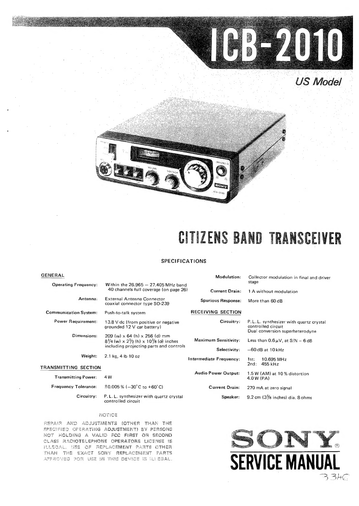
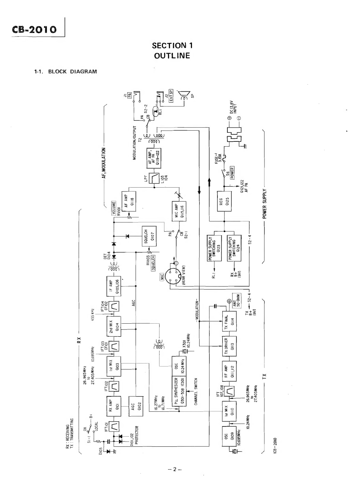
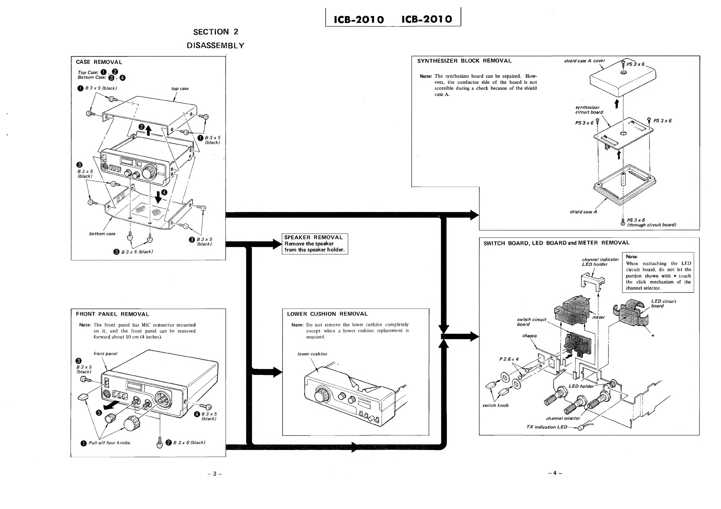
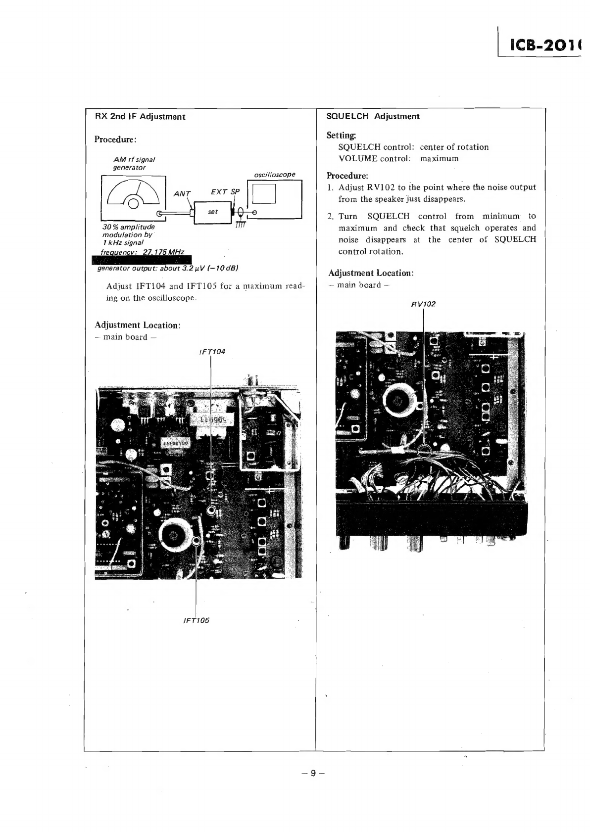