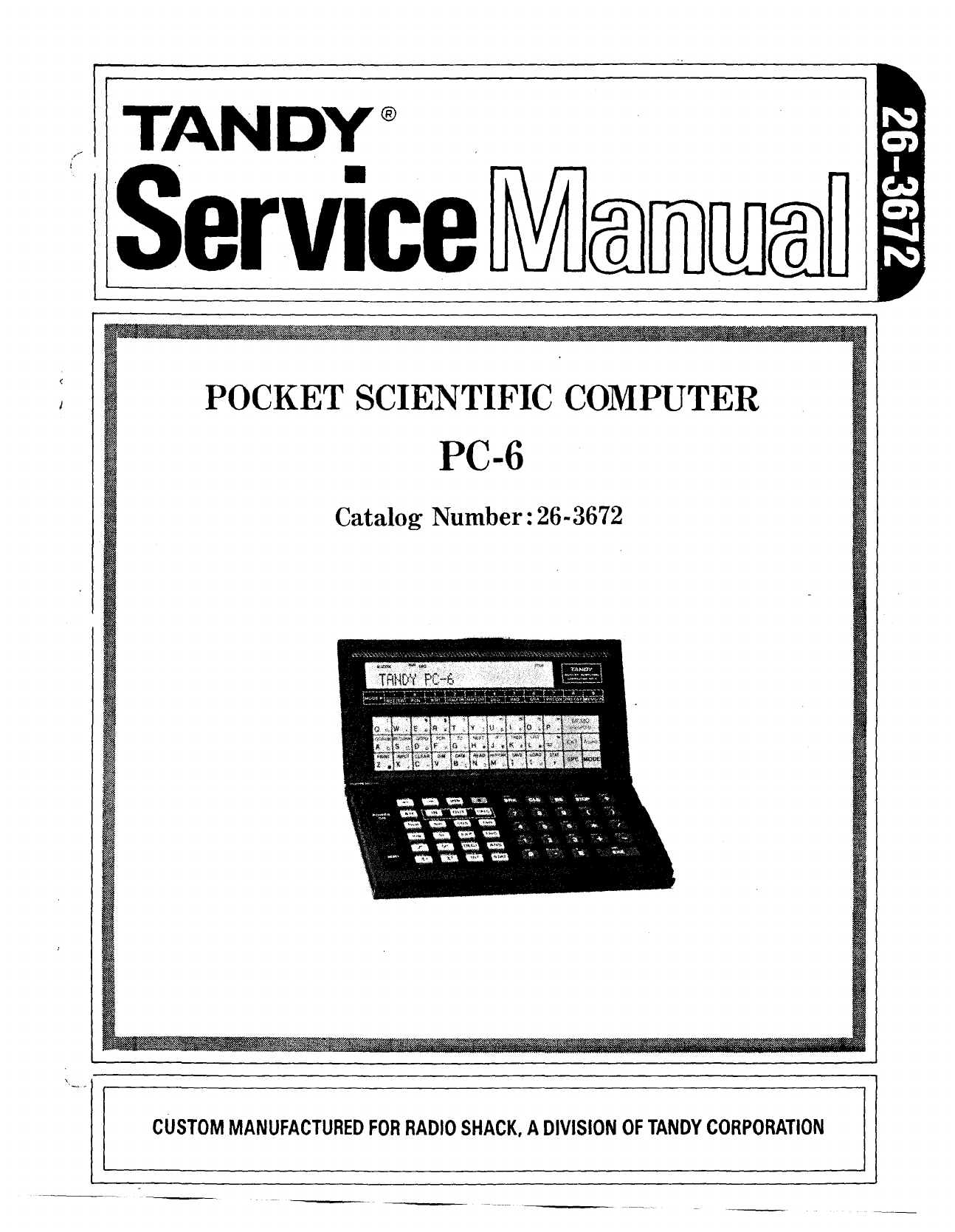
CONTENTS
PAGE
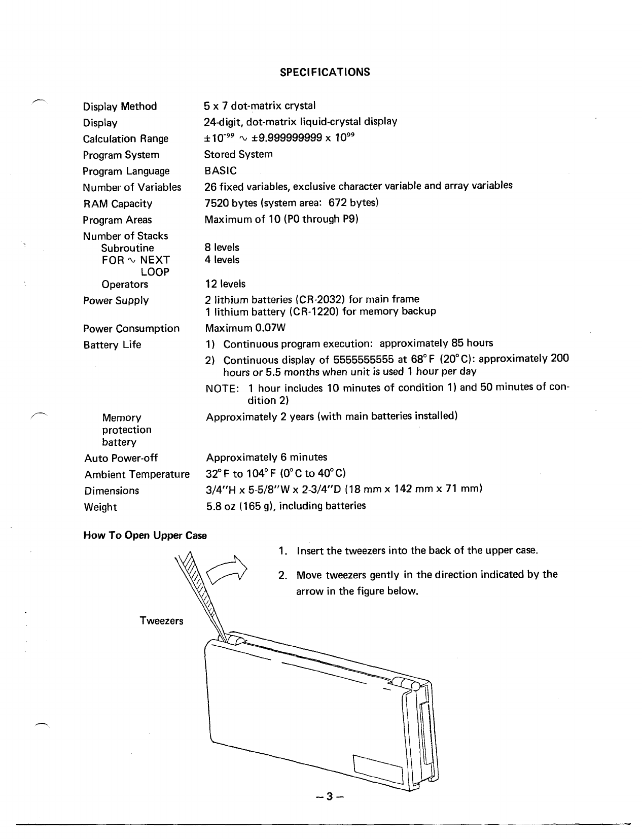
SPECIFICATIONS
•....••..•..•...........•.........•...•....•..•.•........•.•..
3
How
To
Open Upper
Case
....................................•............••..
3
THEORY OF OPERATION
...........•......................•.......••..........
4
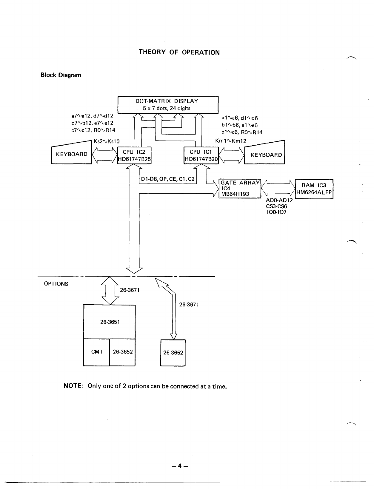
Block Diagram
...•..•••..••••...•.•..........•..•.........•.•.....•.....•••.
4
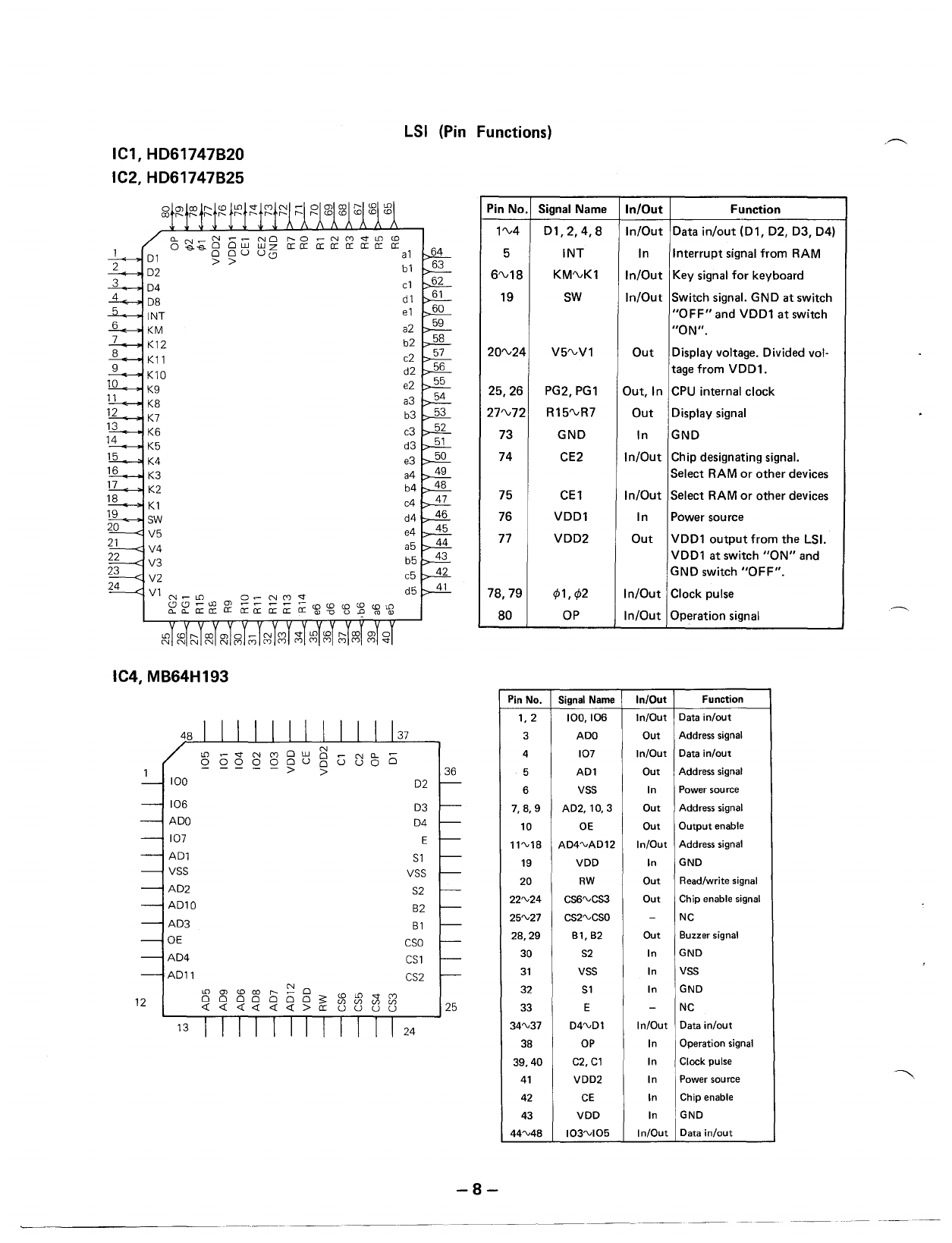
LSI
•.............................
·
......................•.......•.........
5
Ram
Map
...••.....•••..........•...........•........•.......•.............
5
Buzzer Control Circu
it
•..........................................•...........
6
Interrupt Circuit 6
Keyboard
.•.................................................•.........•...
6
Power Supply
........•.....................................................
7
LSI (Pin Functions)
.....•.....•...•.............................................
8
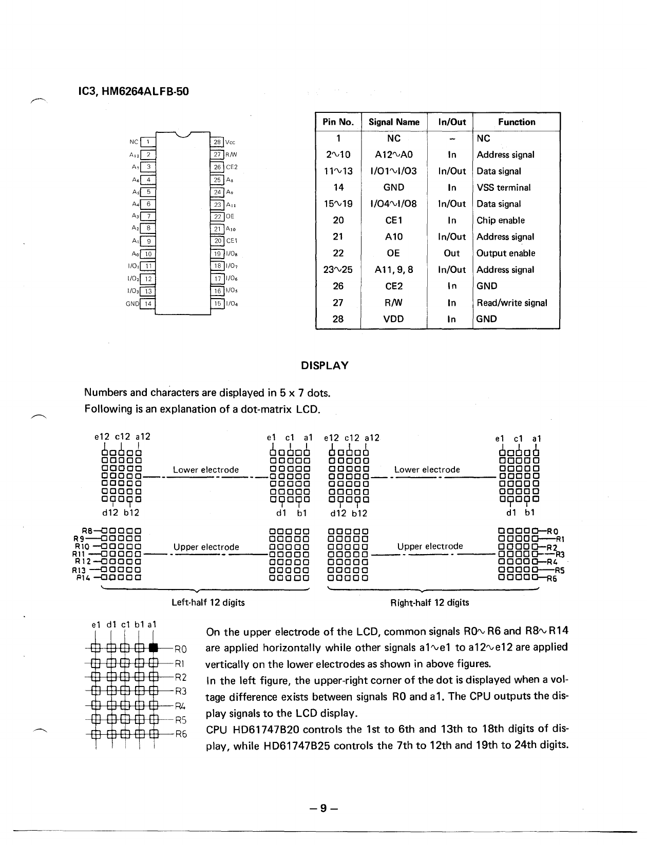
DISPLAY
•..............•..........................................••.........
9
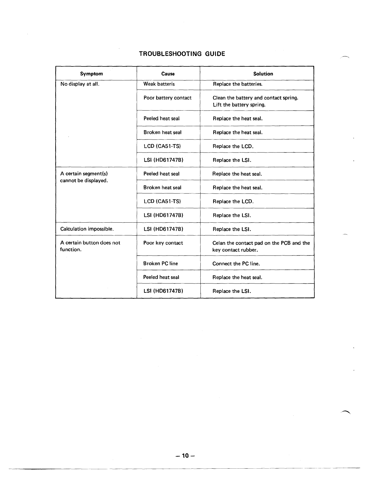
TROUBLESHOOTING GUIDE
.......•...........................................
10
Test Programs
11
Operation Check
........................................•...•.•.•.....•....
14
PCB
ASSEMBLY VIEWS
.......••..........•..•.......•........................
19
PARTS LIST
...........•..•...........................•......................
20
Electrical
Parts
.........•.................•.........•......................
,20
Mechanical Parts
..................•........................................
21
EXPLODED VIEW/DISASSEMBLY INSTRUCTIONS 23
SCHEMATIC
DIAGRAM
...•...•...........•....................................
24
Main Block
..............••........•..•.....•.............................
24
Keyboard
.•....•.••.............••........••..•..........................
25
Display
.........•.•..••..••.....•.•.......•..••..........................
26