Type
7A16
SECTION
2
OPERATING
INSTRUCTIONS
Change information, if any, affecting
this
section
will be found at the
rear of the manual.
General
The
Type
7A16
vertical plug-in
unit
operates
with
a
Tek-
tronix 7000-series oscilloscope and a 7B-series time base
unit
to
form
a complete oscilloscope system.
To
effectively
use
the Type 7A
16,
the operation and capabilities of the
instrument should be
known.
This
section describes the op-
eration of the front-panel controls and connector, gives
first
time operation and general operating information, and
lists
some measurement techniques
using
the amplifier.
Installation
The
Type 7A
16
is
designed to operate
in
a vertical
pl'ug-
in
compartment of Tektronix 7000-series oscilloscopes.
For
X-Y
operation, the plug-in
unit
may also be installed
in
a horizontal plug-in compartment.
(Refer
to the indicator
oscilloscope instruction manual for information concerning
X-
Y operation.)
To
install the Type
7A16
into a plug-in compartment,
push
it
in
until
it
is
seated into the front panel
of
the indicator
unit.
Pull
the release latch to disengage the plug-in
unit,
then continue pulling on the release latch to remove the
plug-in
from
the indicator.
FRONT
PANEL
CONTROLS
AND
CONNECTOR
All
controls required for operation of the Type 7A
16
are
located
on
the front panel of the
unit.
A brief description
of the function or operation of the front-panel controls
fol-
lows.
More detailed information
is
given under General
Operating Information.
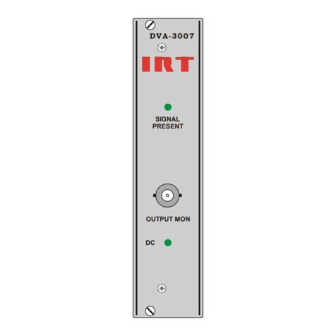
VOlTS/DIV
VARIABLE
(CAL
IN)
POSITION
IDENTIFY
®I
Selects vertical deflection factor
from
5
mV
/DIV
to 5 V
/DIV
in
1-2-5
sequence
(V
AR
control
must
be
in
the calibrated
position for indicated deflection factor).
Provides variable uncalibrated deflection
factors to
at
least 2.5 times the setting of
the
VOLTS/DIV
switch.
Push
knob
in
and
release to activate; the knob moves out-
ward
from
the
VOLTS/DIV
control when
activated.
Controls vertical position of trace.
Moves trace upward about 0.25 division
for identification.
(Also
replaces readout
information
with
the word
IDENTIFY.)
POLARITY
BANDWIDTH
AC-GND-DC
GAIN
STEP
ATTEN
BAL
INPUT
General
Provides means of inverting the display.
+UP: A positive-going voltage
at
the
INPUT
produces a positive de-
flection on the
CRT.
INVERT:
A positive-going voltage
at
the
INPUT
produces a negative de-
flection on the
CRT.
Provides limiting
of
upper bandwidth.
FULL:
Normal operation with
full
band-
width capabilities.
20
MHz:
Amplifier bandwidth limited to
20
MHz
to provide a reduction
in
displayed high-frequency noise
or interference.
Selects method
of
coupling input signal
to
Input Amplifier.
Screwdriver adjustment to set gain of the
amplifier. Gain standardized
at
10
mV
/
Div.
Screwdriver adjustment to minimize trace
shift when switching
VOLTS/DIV
control.
Signal input connector. Input impedance
of 1 megohm paralleled
by
15
picofarads.
Similar to standard
BNC
connector, but
with additional conductor to indicate to
the readout circuit the attenuation factor
of
the probe being used.
FIRST-TIME
OPERATION
When shipped
from
the factory, the Type
7A16
has been
calibrated to meet the specifications listed
in
Section 1 and
is
ready to be used with an indicator oscilloscope.
The
following steps demonstrate the basic operation
of
the controls
of
the Type
7A16.
It
is
recommended that
this
procedure be followed completely for familiarization with
the instrument. Operation of the indicator oscilloscope and
time base
unit
is
described
in
the instruction manuals
for
these
units.
Setup
Information
1.
Insert the Type 7A
16
into a vertical plug-in compart-
ment of a 7000-series indicator oscilloscope.
2.
Insert a 7B-series time-base
unit
into a horizontal plug-
in
compartment.
3.
Set the controls as follows:
2-1
