L
Type 7A14
SECTION
2
OPERATING
INSTRUCTIONS
Change
information,
if
any,
affecting
this section
will
be
found
at
the
rear
of
the
manual.
General
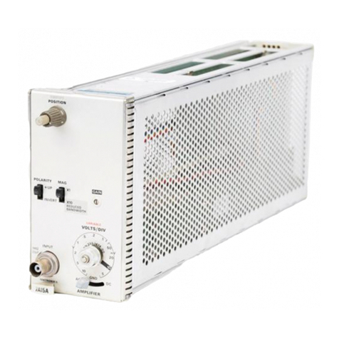
The Type 7A14 vertical plug-in unit
operates
with a Tek-
tronix 7000-series indicator oscilloscope, a 7B-series time
base
unit,
and
Tektronix
P6021
or
P6022 Current Probes to
form a complete current measuring system. To effectively
use the Type 7A14, the operation
and
capabilities of the
instrument should
be
known. This section describes the op-
eration of the front-panel controls, gives first-time operation
and
general operating information,
and
lists some measure-
ment techniques using the current probes.
Installation
The Type 7A14
is
designed to
operate
in
a vertical plug-
in
compartment of Tektronix 7000-series oscilloscopes. For
X-Y
operation, the plug-in unit may also be installed
in
a
horizontal plug-in compartment. (Refer to the indicator os-
cilloscope instruction manual for information concerning
X-Y
operation.)
To
install the Type 7A14 into a plug-in compartment, push
it
in
until it
is
seated
against
the front panel
of
the indicator
oscilloscope.
To
remove, pull the release latch to
disengage
the plug-in unit from the indicator oscilloscope. Continue to
pull the release latch to remove the unit from the oscilloscope.
FRONT-PANEL
CONTROLS
AND
CONNECTORS
All
controls
and
the connector required for operation of
the Type 7A14
are
located on the front panel of the unit (see
Fig.
2-1). A brief description of the function
or
operation of
the front-panel controls
and
the connector follows. More
detailed information
is
given under
General
Operating
Information.
CURRENT
IDIV
Selects vertical deflection factor from 1
mAIDiv
to 1 AMP/DIV
in
1-2-5 sequence
(VAR
control must
be
in
the calibrated
position for indicated deflection factor).
VAR
(CAL
IN)
POSITION
IDENTIFY
POLARITY
Provides variable uncalibrated deflection
factors to
at
least 2.5 times the setting of
the
CURRENT
IDIV switch. Push knob
in
and
release to activate; the knob moves
outward from the
CURRENT
IDIV control
when activated.
Controls vertical position of trace.
Moves trace upward
about
0.25 divisions
for identification. Also identifies the read-
out
corresponding
to
the Type 7A14.
Provides means of inverting the display.
BANDWIDTH
LF
COMP
GAIN
NORM:
INVERT:
Conventional current flowing
in
the direction of the
arrow
on the
probe
(see
Fig.
2-2)
pro-
duces a positive deflection
on
the
CRT.
Conventional current flowing
in
the direction of the arrow
on the
probe
produces a neg-
ative deflection on the
CRT.
Provides limiting of
upper
bandwidth.
FULL:
20 MHz:
Normal operation with
full
bandwidth capabilities.
Amplifier bandwidth limited
to 20 MHz to provide a re-
duction
in
displayed high-fre-
quency noise
or
interference.
Screwdriver adjustment to compensate low-
frequency response.
Screwdriver adjustment to set the gain of
the amplifier. The 10
mA
position
is
color
shaded
to indicate
that
the GAIN should
be
adjusted
in
this position of the switch.
CURRENT
PROBE
Signal input connector. Similar to standard
INPUT
BNC
connector, but with additional con-
ductor.
When
the
P6021
probe
is
con-
nected to the input, the additional con-
ductor
is
shorted to ground by the probe
connector, actuating relays
in
the Type
7A14 to set the gain
and
peaking circuits
to correspond with the
P6021
probe.
NOTE
P6021
probes
with
regular
BNC
connector
must
be
modified
with
a
special
coding
ring
to
be
compat-
ible
with
the
7
-series
plug-in
units.
Contact
your
local
Tektronix
Field
Office
or
Representative
for
assistance
in
procuring
the
coding
ring.
FIRST-TIME
OPERATION
General
When
shipped from the factory, the Type 7A14 has been
calibrated to meet the specifications listed
in
Section 1
and
is
ready
to
be
used with
an
indicator oscilloscope.
The following steps demonstrate the basic operation of
the controls
and
connectors of the Type 7A14.
It
is
recom-
mended
that
this procedure
be
followed completely for
familiarization with the instrument.
Operation
of
the indi-
cator
oscilloscope
and
time
base
unit
is
described
in
the
instruction manuals for those units.
2-1
