1 Overview
1.1 Purpose
1.2 EVM Basic Functions
1.3 Power Requirements
1.4 ADS-ADX EVM Operational Procedure
www.ti.com
Overview
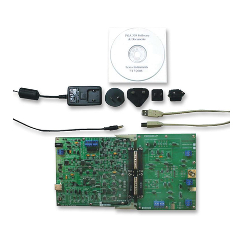
This user’s guide gives a general overview of the ADS-ADX Evaluation Board for interleaving (later calledADS-ADX EVM). It provides a description of the features and functions to consider when using themodule.
The ADS-ADX EVM provides a platform for evaluating two interleaved ADS5474 analog-to-digitalconverters (ADC) with a combined sampling rate of 800 MSPS. The ADS5474 is a 14-bit, 400-MSPS ADCwhich is pinout compatible with the ADS5463, a 12-bit, 500-MSPS ADC. For a more in-depth theoreticaldescription of ADC interleaving, consult the white paper Frequency-Response Mismatch Errors and DigitalCorrection in Time-Interleaved ADCs – available at www.spdevices.com . For system design with thistechnology, consult the SP Devices application note Recommended Analog Front-End Design for ADXwith ADS5474/ADS5463. The ADS-ADX EVM contains an ADC interleaving IP core from SP Devices. Forcommercial information and available platforms, contact SP Devices.
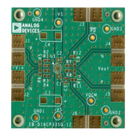
One analog input into the EVM is provided via the SMA connector. The input is AC-coupled, and the usersupplies a single-ended input signal, which is converted into a differential signal at the input. TheADS-ADX EVM provides an SMA connector for input of the ADC clock. The external clocking interface isto be clocked with a 50% duty cycle clock, at half of the sampling rate of the interleaved system samplingrate.
The interleaving and digital post-correction (ADX IP-core) is implemented in real time using the Virtex-5FPGA on the board.
Digital output from the EVM is provided both by two Soft Touch Probe (support for Agilent E5405A andTektronix P6908 probes) connectors for logic analyzers and by a USB connector for connecting apersonal computer. The USB interface samples the data into internal FPGA memory, which has amaximum depth of 65,536 samples.
The ADS-ADX EVM is powered through the 6-Vdc power supply adapter that is supplied. Powerconsumption during operation is approximately 12 W for the board.
1. Verify the DIP switch settings to reflect your intended setup (Section 2.5 and Table 2 )2. Connect the supply power to the EVM, from the supplied mains adapter.3. Press the reset button.4. Use a 50- Ωfunction generator with an output swing of ±1 V at the clocking speed of half the fullsystem, with a duty cycle of 50% ( ±3%).5. Connect a 50- Ωfunction generator with a 55-MHz, 0-V offset, 700-mV amplitude sine wave to the inputof the ADC channel.6. The digital output pattern on the Soft Touch Probe connector now represents a sine wave and can bemonitored with a logic analyzer.7. Or connect a USB cable between the board and your computer, start the program ADCaptureLab(installation: see section Software), and collect the data. The plots provided are a time-series plot andan FFT of the signal.
SLAU247 – August 2008 ADS5474 ADX Evaluation Board for Interleaving 3Submit Documentation Feedback
