ACTiSYS IR8250P User manual

48511 Warm Springs Blvd., Suite 206, Fremont, CA 94539
Tel: (510) 490-8024 Fax: (510) 623-7268
Website: http://www.actisys.com E-mail: irda-info@actisys.com
ACT-IR8250P
IrDA Compliant Protocol Processor
Specification
© Copyright 2003-2005 ACTiSYS Corporation
All Rights Reserved
January 28, 2005 Rev. 0.44

The Infrared Wireless Expert ACT-IR8250P
Specification
Revision History
Revision Date Comment
Rev. 0.1 08/21/2003 Preliminary Design Specification
Rev. 0.2 08/26/2003 Removed Chapter 5 and added Appendix 1
Rev. 0.3 12/08/2003 Updated reference circuit & IrDA transceiver model #. Updated
implementation examples. Added Eval. Kit PCB dimensions
and circuit schematics.
Rev. 0.31 12/19/2003 Updated reference circuit in more detail.
Rev. 0.4 01/12/2004 Revised Appendix 1 for Development Kit.
Rev. 0.41 03/31/2004 Revised IR8250SW statement in Appendix 1.
Rev. 0.42 04/23/2004 Add In-system programming in chapter 9.
Rev. 0.43 11/22/2004 Add connector of DB dimension on page 16.
Rev. 0.44 01/28/2005 Add IR8250PEK-J1 connector detail on pages 16~19 & 21
© Copyright 2003-2005 ACTiSYS Corp. Page 1 of 25 Jan 28, 2005
Rev. 0.44

The Infrared Wireless Expert ACT-IR8250P
Specification
Table of Contents
1. Features ......................................................................................................................... 3
2. Overview ........................................................................................................................ 5
3. PIN Description..............................................................................................................6
4. Device Operation........................................................................................................... 8
5. IrDA Protocols Supported .......................................................................................... 10
6. IR8250P Parts ID and Firmware Number System...................................................... 11
7. Connect ACT-IR8250P to a Host Device with RS232 Port ........................................ 12
8. Implementation Notice ................................................................................................ 13
9. In-System Programming in ACT-IR8250P.................................................................. 14
10. ACT-IR8250P Evaluation Kit (IR8250PEK and IR8250PEKK) ................................. 15
11. Characteristics and Specification ............................................................................ 20
12. Application Circuit..................................................................................................... 21
13. Package Dimensions................................................................................................. 22
Appendix 1. How To Use ACT-IR8250PEK (ACT-IR8250P Evaluation Kit): ................. 24
© Copyright 2003-2005 ACTiSYS Corp. Page 2 of 25 Jan 28, 2005
Rev. 0.44

The Infrared Wireless Expert ACT-IR8250P
Specification
1. Features
A complete IrDA Protocol stack in a single chip, includes mandatory protocols (IrPHY, IrLAP,
IrLMP) and optional protocols (IrLPT, IrCOMM+TinyTP, OBEX transport or TinyTP with
customized IAS class name for IrSocket).
Also Includes IrPHY encoding/decoding, and interfaces directly to Infrared transceivers for data
rate from 9.6kbps up to 115.2kbit/s. Only an external Infrared transceiver is needed to complete
an IrDA compliant infrared communication subsystem.
ACT-IR8250P supports IrDA Secondary mode only.
Supports 64 bytes data packet for IrDA IrLAP frame.
Interfaces to Host device via a full function UART port.
Supports host baud rate from 300kbit/s to 115.2kbit/s selecting by programmable settings.
Programmable Device name, IAS class name and data format setting.
Available in programmed and tested chip (IR8250P), assembled & tested board (IR8250PDB),
or assembled & tested evaluation kit (IR8250PEK).
Low supply voltage, 3.0 V to 3.6 V.
Low current consumption; 2uA standby, 3mA active.
Small low profile plastic 28-pin SSOP/TSSOP package.
In-system-programmable FLASH, facilitates firmware changes or updates.
The evaluation kit (IR8250PEK) includes AC power supply, RS232 level translators, and PC
software for in-system re-programming of firmware and future firmware options.
ACT-IR8250PEK consists of: IR82x0PMB (motherboard) + IR8250PDB +
Self-downloadable SW to program IR8250P firmware.
1) IR82x0PMB: RS232 level converter, DB9 connector, probe pins and IR8250PDB connector.
2) IR8250PDB (daughter board for direct connection to your embedded PCB):
Self-contained full-function IrDA module, which consists of: IR8250P protocol IC +
IrDA transceiver + 3.3V interface connector.
A very useful “Evaluation Kit Full Set” is ACT-IR8250PEKK, which is: IR8250PEK + IR4000US
(notebook/desktop USB-IrDA adapter). This is to test IR8250P (connected to your device),
to exchange IrDA data with IR4000US (connected to PC USB port), running hyper-terminal
on top of Windows IrDA driver. To avoid debugging multiple issues: e.g. PDA application
IrDA SW activated and behaves properly, with the matching protocol layer? IR8250P to host
interface issues (UART data rates, flow control, data bit/parity/stop bit, UART signal pins, power
levels)? Performance issues (throughput, distance, error rate/dropping bits)?
© Copyright 2003-2005 ACTiSYS Corp. Page 3 of 25 Jan 28, 2005
Rev. 0.44

The Infrared Wireless Expert ACT-IR8250P
Specification
ACT-IR8250P
© Copyright 2003-2005 ACTiSYS Corp. Page 4 of 25 Jan 28, 2005
Rev. 0.44

The Infrared Wireless Expert ACT-IR8250P
Specification
2. Overview
The ACT-IR8250P is a low cost, small pin-count, high-integration and in-system-programmable
micro-controller, with on-chip IrDA protocol stack and on-chip Infrared physical encoder/decoder. It
provides a serial interface to a host device that intends to have Infrared communication capability.
The host device can be any equipment or device that needs to communicate with IrDA enabled
portable or tablet PC, PDA, cellular phone and hand held data terminal, via IrDA beam and protocol
but has only a wired serial interface. The ACT-IR8250P will handle all the detail about IrDA protocol.
It sends/receives only user data to/from the host device via the wired serial interface with hardware
flow-control. IrDA has two modes; one is Primary, and the other is Secondary. The difference
between these two modes is that a Primary mode device initiates the discovery, negotiation and
connection sequence to Secondary mode device, and decides IrDA protocol parameters. Secondary
mode device always waits for commands from Primary mode device. Both modes can run different
protocols, and both may send or receive user data. ACT-IR8250P supports Secondary mode only.
Fig.1 is system diagram.
© Copyright 2003-2005 ACTiSYS Corp. Page 5 of 25 Jan 28, 2005
Rev. 0.44

The Infrared Wireless Expert ACT-IR8250P
Specification
3. PIN Description
Symbol Pin
No.
I/O
Type Descriptions
TEST 1 I Reserved. Pull low with 30k ohm resistor.
VCC 2 Pwr Digital supply voltage, positive terminal.
P2.5 3 I/O Reserved. Pull high with 30k ohm resistor.
VSS 4 Digital supply voltage, negative terminal. Ground,
XOUT 5 I/O Output terminal of crystal oscillator.
XIN 6 I
Input port for crystal oscillator. Standard crystals can be
connected.
nRST/NMI 7 I Reset input. (n: Active low )
P2.0/nEnable 8 I
Power control from Host. (n: Active low )
High=Power down IR8250P, Low=Enable and power on.
P2.1/IR_SD 9 O
Shut down transceiver.
High=Shut down, Low=Enable.
P2.2/STOP_TX 10 I
TX flow control from host.
High=Host not ready to accept TX,
Low=Host ready to accept TX.
P3.0 11 I/O Reserved. Keep it open.
P3.1 12 I/O Reserved. Keep it open.
P3.2 13 I/O Reserved. Keep it open.
P3.3 14 I/O Reserved. Keep it open.
P3.4/TX 15 O
Serial data to Host.
High=Idle / Stop bit / 1-bit. Low=Start bit / 0-bit.
P3.5/RX 16 I
Serial data from Host.
High=Idle / Stop bit / 1-bit. Low=Start bit / 0-bit.
P3.6 17 I/O Reserved. Keep it open.
P3.7 18 I/O Reserved. Keep it open.
P2.3/IR_TX 19 O
Transmit data to transceiver.
High= IR on, Low=IR off.
P2.4 20 I/O Reserved. Keep it open.
P1.0/Status 21 O
IrDA status to Host.
High=No IrDA connection. Low=IrDA connection active.
P1.1/STOP_RX 22 O RX flow control to Host.
High=IR8250P not ready to accept RX, Low=IR8250P ready to
P1.2/nIR_RX 23 I
Received data from transceiver. (n: Active low )
High=No IR, Low=IR detected.
© Copyright 2003-2005 ACTiSYS Corp. Page 6 of 25 Jan 28, 2005
Rev. 0.44

The Infrared Wireless Expert ACT-IR8250P
Specification
PIN Description (Continued)
Symbol Pin
No.
I/O
Type Descriptions
P1.3 24 I/O Reserved. Keep it open.
P1.4 25 I/O Reserved. Keep it open.
P1.5 26 I/O Reserved. Keep it open.
P1.6 27 I/O Reserved. Keep it open.
P1.7 28 I/O Reserved. Keep it open.
© Copyright 2003-2005 ACTiSYS Corp. Page 7 of 25 Jan 28, 2005
Rev. 0.44

The Infrared Wireless Expert ACT-IR8250P
Specification
4. Device Operation
4.1 RESET circuit
IR8250P will be reset when nRST is pulled low.
It needs a 100K ohms resistor, 0.1uF capacitor
and a diode to implement the reset circuit.
Please refer to right figure.
4.2 Crystal circuit
IR8250P needs a specified clock to operate,
please refer to right figure.
4.3 Host Interface
The host interface of IR8250P is a full-duplex asynchronous serial data interface. The data bytes are
transmitted via TX and received via RX. Each data byte consists of one start bit (0), 8 data bits (LSB
first, MSB last) and a stop bit (1).
© Copyright 2003-2005 ACTiSYS Corp. Page 8 of 25 Jan 28, 2005
Rev. 0.44

The Infrared Wireless Expert ACT-IR8250P
Specification
4.4 IR port interface
The IR port of IR8250P can be connected to most transceiver. The data is transmit by pin IR_TX and
data received by nIR_RX. IR_SD can shut down transceiver when IR8250P is disabled. This pin is
optional. The below figure is the signal specification of IR_TX, it sends 1.63uS pulse infrared signal
out.
© Copyright 2003-2005 ACTiSYS Corp. Page 9 of 25 Jan 28, 2005
Rev. 0.44

The Infrared Wireless Expert ACT-IR8250P
Specification
4.5 Operating modes
When nEnable is high, ACT IR8250P drives IR_SD high (to shutdown the IR transceiver) and puts
itself to sleep. In this sleep state, it can be awaken only by nEnable going low.
When nEnable is low, ACT IR8250P drives IR_SD low (to power up the IR transceiver) and puts itself
to sleep. In this sleep state, it can be awaken by any incoming IR signal. Once awaken, it will either
actively communicate with an IrDA Primary device (PC, PDA, Cell phone, etc.), or go back to sleep if
no IrDA Primary is there.
5. IrDA Protocols Supported
The following figure is the block diagram of ACT-IR8250P protocols architecture. The red colored
blocks represent different optional upper layers. Only one of the red colored blocks can be included
at a time.
IrLMP and IAS
IrLAP
IrLPT or IrCOMM 3-wire raw
IrCOMM 9-wire
Host Interface
IrPHY
Host Interface
ACT-IR8250P TinyTP
OBEX Transport
IrDA Transceiver
IrSocket
Host
© Copyright 2003-2005 ACTiSYS Corp. Page 10 of 25 Jan 28, 2005
Rev. 0.44

The Infrared Wireless Expert ACT-IR8250P
Specification
7. Connect ACT-IR8250P to a Host Device with RS232 Port
Devices that use serial cables for their communication are split into two categories. These are DCE
(Data Communications Equipment) and DTE (Data Terminal Equipment.) Data Communications
Equipment is device such as your modem, TA adapter, plotter etc while Data Terminal Equipment is
your Computer or Terminal. The following shows how to connect IR8250P to a DTE and a DCE.
Note: A RS232 level converter chip is needed when IR8250P is connected to a RS232 interface.
There are a total of 7 signals between the host and the IR8250P. The pin assignment and name of
each signal at the chip levels are summarized in Table 1 below. Please note that DTE denotes
signals on the RS232 board or device. In order to connect them to another DTE, a null-modem
converter is used in-between. The pin assignment and name are listed in this table.
Table : Host interface signals
ACT-IR8250P RS232 DTE device RS232 DCE device
Pin No. Type Name Pin No. Type Name Pin No. Type Name
15 O TX 2 I RX 3 I RX
16 I RX 3 O TX 2 O TX
8 I nEnable 4 O DTR 6 O DSR
21 O Status 6 I DSR 4 I DTR
10 I STOP_TX 7 O RTS 8 O CTS
22 O STOP_RX 8 I CTS 7 I RTS
4 GND 5 GND 5 GND
© Copyright 2003-2005 ACTiSYS Corp. Page 12 of 25 Jan 28, 2005
Rev. 0.44

The Infrared Wireless Expert ACT-IR8250P
Specification
8. Implementation Notice
Following signals lists the description of implementation notes when designed into board.
(1) Power supply
Pin Name Comments
2 VCC Digital power. Connect a 0.1uF bypass capacitor at this pin.
4 VSS
Digital ground
(2) Crystal Oscillator
Pin Name Comments
6 XTIN Input port for crystal oscillator. Only standard crystals can be connected.
5 XTOUT Output terminal of crystal oscillator
Both of these two pins connect a 20pF capacitor.
(3) Reset
Pin I/O type Name Comments
7 I nRST
Active low reset. This signal can be generated by the host, a RC
circuit or a RESET chip. It supports Brown-out feature.
(4) IrDA Transceiver
Pin I/O type Name Comments
19 OIr_TX IrDA Transmitter, high active. Connect to TXD pin of IrDA transceiver.
23 I nIr_RX IrDA Receiver, active low. Connect to RXD pin of IrDA transceiver.
9 O IR_SD Transceiver power control.
Please see the transceiver’s specification to get more detail information about transceiver.
Place IR8250P chip next to transceiver module as close as possible. And keep chip away from high
power consumption components.
© Copyright 2003-2005 ACTiSYS Corp. Page 13 of 25 Jan 28, 2005
Rev. 0.44
The Infrared Wireless Expert ACT-IR8250P
Specification
9. In-System Programming in ACT-IR8250P
ACT-IR8250P supports In-system Programming, it is useful to upgrade firmware of IR8250P if IrDA
protocol, host baud rate or data format requested to be changed on target board (Please refer to
IR8250SW to get more detail operations). To implement ISP, there are some signals needed to do
the following,
(1) Status (output) at Pin-21 (P1.0) of IR8250P must be converted to RS232 Level and connected to
the DSR input of PC COM Port.
(2) Stop_Rx (output) at Pin-22 (P1.1) of IR8250P must be converted to RS232 Level and connected
to the CTS input of PC COM Port.
(3) Tx (output) at Pin-15 (P3.4) of IR8250P must be converted to RS232 Level and connected to the
RxD input of PC COM Port.
(4) PC COM Port DTR (output) must be converted to 3.3V Logic Level and connected to Enable
(input) at Pin-8 (P2.0) of IR8250P. This signal line must not be driven by any other circuit.
(5) PC COM Port RTS (output) must be converted to 3.3V Logic Level and connected to Stop_Tx
(input) at Pin-10 (P2.2) of IR8250P. This signal line must not be driven by any other circuit.
(6) PC COM Port TxD (output) must be converted to 3.3V Logic Level and connected to Rx (input) at
Pin-16 (P3.5) of IR8250P. This signal line must not be driven by any other circuit.
(7) Ground (Pin-4) of IR8250P, ground of RS232 Level converter, and ground of PC must be
connected together.
(8) You must power-up the IR8250P after the PC program "IR8250SW" informs you to "Remove J10"
and before you click at "OK".
© Copyright 2003-2005 ACTiSYS Corp. Page 14 of 25 Jan 28, 2005
Rev. 0.44
The Infrared Wireless Expert ACT-IR8250P
Specification
10. ACT-IR8250P Evaluation Kit (IR8250PEK and IR8250PEKK)
It is recommended that customer verify the compatibility with your host system by using
ACT-IR8250P evaluation kit, IR8250PEK. It is a self-contained unit, with ACT-IR8250P, IrDA
transceiver, RS232-level converter and external AC power connector, all built into a compact
package. ACT-IR8250 evaluation kit enables your host system to be IrDA (IrReady) certifiable,
immediately. Moreover, this kit can be a full PCB with RS232 interface, or as half-PCB with UART
interface, without the burden of RS232 interface circuitry.
ACT-IR8250PEK package consists of: IR82x0PMB (motherboard) + IR8250PDB
+ Self-downloadable SW to program IR8250P firmware.
1) IR82x0PMB: RS232 level converter, DB9 connector, probe pins and IR8250PDB connector.
2) IR8250PDB (daughter board for direct connection to your embedded PCB):
Self-contained full-function IrDA module, which consists of: IR8250P protocol IC +
IrDA transceiver + 3.3V interface connector.
A more useful Evaluation Kit Full Set is ACT-IR8250PEKK, which is: IR8250PEK + IR4000US
(notebook/ desktop USB-IrDA adapter). This is to test IR8250P (connected to your device), to
exchange IrDA data with IR4000US (connected to PC USB port), running hyper-terminal (assigned
to the same virtual comm port as the one used by Windows IrDA driver) on top of Windows IrDA
driver. This avoids debugging multiple issues: PDA application issues (IrDA SW activated and
behaves properly)? IR8250P to host interface issues (UART data rates, flow control, data
bit/parity/stop bit, signal pins, power levels)? Performance issues (throughput, distance, error
rate/dropping bits)?
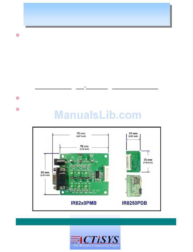
The following figure is IR8250P evaluation kit, IR8250PEK. It consists of two boards, IR82x0PMB on
the left, and IR8250PDB on the right, connected to each other by 10 pin connector/cable. You can
connect this evaluation kit to your host RS232 port, or use IR8250PDB board to connect to your host
CMOS level UART signals.
The corresponding circuit schematics for IR82x0PMB and IR8250PDB are also included below.
The detail User’s Guideline is described in Appendix 1. How to use IR8250PEK?
© Copyright 2003-2005 ACTiSYS Corp. Page 15 of 25 Jan 28, 2005
Rev. 0.44
The Infrared Wireless Expert ACT-IR8250P
Specification
ACT-IR8250PEK PCB Photos and Dimensions:
PCB footprint & dimensions, part number, supplier and pinout spec for the connector J1 on
IR8250x0PMB and IR8250PDB boards are as follows: Molex, part number SD-48148, you
can get dimensional information at: www.molex.com. More details on page 17.
© Copyright 2003-2005 ACTiSYS Corp. Page 16 of 25 Jan 28, 2005
Rev. 0.44
The Infrared Wireless Expert ACT-IR8250P
Specification
J1 Connector: CONN JST(M) 10Pin
© Copyright 2003-2005 ACTiSYS Corp. Page 17 of 25 Jan 28, 2005
Rev. 0.44

The Infrared Wireless Expert ACT-IR8250P
Specification
ACT-IR8250PEK Circuit Schematics:
1) ACT-IR82x0PMB Motherboard Circuit Schematic:
1 2 3 4 56
A
B
C
D
6
54321
D
C
B
A
Title
Number RevisionSize
B
Date: 19-Dec-2003 Sheet of
File: D:\data\IR8240-8250_EVA\IR8250_03\20031105_IR8250_(IR82x0PEK).ddbDrawn By:
V+ 1
V-
25
VCC 3
GND 5
GND
27
D IN1 7
D IN2 8
D IN3 9
D OUT1
22
D OUT2
21
D OUT3
20
R OUT1 10
R OUT2 11
R OUT3 12
R OUT4 13
R OUT5 14
R IN1
19
R IN2
18
R IN3
17
R IN4
16
R IN5
15
C1-
24
C2- 4
C2+ 2
C1+ 6
C3+
28
C3-
26
SD
23
U1
75LV4737A
1
6
2
7
3
8
4
9
5
J2
DB9/F
C7
0.1u
C8
0.1u
C6
10u
C9
10u
Vin
3
Gnd
2
Vout 1
U2
AIC1722-33CX
5-12VDC
P1
DC POWER JACK
1
2
J10
+
C1 0.47uF
C3
470nF/16V
C4
470nF/16V
C2
470nF/16V
C5
470nF/16V
DSR
RxD
CTS
RTS
TxD
DTR
IR82x0PEK Board
Yuwei
1
2
J11
ACTISYS CORP.
CONFIDENTIAL
Copyright (C) 2003-2003 ACTiSYS Corp. 0.3
D8D7
R1
1k
R4
1k
D10D9
R5
1k
R8
1k
D12D11
R9
1k
R12
1k
D1 D2
R3
1k
R2
1k
D3 D4
R7
1k
R6
1k
D5 D6
R11
1k
R10
1k
DSR
RxD
CTS
RTS
TxD
DTR
Vcc
TEST
nRST
1
2
3
J3
RTS
1
2
3
J4
TxD
1
2
3
J5
DTR
RTS
TxD
DTR
1
2
3
4
5
6
7
8
9
10
J1
Link to IR8250/8200/8240PDB boards
+ +
+3.3V
+3.3V
Status
Tx (to host Rx)
Stop_Rx
Stop_Tx
Rx (from host Tx)
nEnable
+3.3V
Stop_Rx
Status
Stop_Tx
nEnable
Rx (from host Tx)
Tx (to host Rx)
PCB footprint & dimensions, part number, supplier and pinout spec for the connector J1 on
IR8250x0PMB and IR8250PDB boards are as follows: Molex, part number SD-48148, you
can get dimensional information at: www.molex.com. More details on page 17.
© Copyright 2003-2005 ACTiSYS Corp. Page 18 of 25 Jan 28, 2005
Rev. 0.44

The Infrared Wireless Expert ACT-IR8250P
Specification
2) ACT-IR8250PDB Daughter Board Circuit Schematic:
(Same as Application Reference Circuit in Section 11)
If your design uses daughter board configuration for convenient placement against front panel,
with cable connection to your system board, it is advisable for you to maintain the 10 pin connector as
in this ACT-IR8250PDB reference circuit here. This enables in-system IR8250P firmware
re-programming with new firmware if such need arises. This flexibility can extend your product
lifetime, improve compatibility with new IrDA devices, add or change IrDA functionality, indeed a
valuable and useful feature.
1 2 3 4 56
A
B
C
D
6
54321
D
C
B
A
Title
Number RevisionSize
B
Date: 19-Dec-2003 Sheet of
File: D:\data\IR8240-8250_EVA\IR8250_03\20031105_IR8250_(IR82x0PEK).ddbDrawn By:
IR8250PDB Board
Yuwei
ACTISYS CORP.
CONFIDENTIAL
Copyright (C) 2003-2003 ACTiSYS Corp. 0.3
X1
7.3728MHz
C2 20pF
C1 20pF
C4
0.1uF
C3
0.1uF
R1 30k
R2
100k
IR_TX
IR_RX
/RST
D1
1N4148
IR_SD
NAME I/O DESCRIPTION USAGE
TX
RX
STOP_RX
STOP_TX
Status
Enable
O
O
O
I
I
I
Serial data to host
Serial data from host
RX Flow-control to host
TX Flow-control from host
Status to host
Enable from host
High = idle / stop-bit / 1-bit
Low = start-bit / 0-bit
High = idle / stop-bit / 1-bit
High = IR8250P not ready to accept RX
Low = IR8250P ready to accept RX
High = Host not ready to accept TX
Low = Host ready to accept TX
High = no IrDA connection
Low = IrDA connection active
High = disallow IrDA connection
Low = allow IrDA connection
R5 30k
TEST
1
VCC
2
P2.1 9
P1.5 26
P2.5 3
VSS
4
XOUT
5
XIN
6
RST/NMI
7
P2.0 8
P2.2 10
P2.3 19
P2.4 20
P1.0 21
P1.1 22
P1.2 23
P1.3 24
P1.4 25
P1.6 27
P1.7 28
P3.0 11
P3.1 12
P3.2 13
P3.3 14
P3.4 15
P3.5 16
P3.6 17
P3.7 18
U1
IR8250P Warning: very sensitive to EMI.
C5
0.1uF
R3
30k
C6
4.7uF/16V
for low power
IREDA
1IREDC
2TXD
3RXD
4SD
5VCC
6
GND
8
Vlog
7
IR1
TFDU4300
R4 47R
IR_RX
IR_TX
IR_SD
Vcc
GND
1
2
3
4
5
6
7
8
9
10
J1
Link to IR82x0PEK board
TEST
/RST
R6
470R
LD1
LED
+3.3V
+3.3V
+3.3V +3.3V
+
+3.3V
Status
Stop_Rx
Stop_Tx
Enable
Rx (from host Tx)
Tx (to host Rx)
Stop_Rx
Status
Stop_Tx
Enable
Rx (from host Tx)
Tx (to host Rx)
+3.3V
+3.3V
PCB footprint & dimensions, part number, supplier and pinout spec for the connector J1 on
IR8250x0PMB and IR8250PDB boards are as follows: Molex, part number SD-48148, you
can get dimensional information at: www.molex.com. More details on page 17.
© Copyright 2003-2005 ACTiSYS Corp. Page 19 of 25 Jan 28, 2005
Rev. 0.44
Other manuals for IR8250P
2
This manual suits for next models
1
Table of contents
Other ACTiSYS Computer Hardware manuals
Popular Computer Hardware manuals by other brands

Klark Teknik
Klark Teknik DN32-USB quick start guide

ADLINK Technology
ADLINK Technology COM Express Type 7 Starter Kit Plus quick start guide

ekwb
ekwb EK-PRO GPU WB H100 Rack - Nickel + Inox user guide

Clover Systems
Clover Systems DVX-4 operating manual

Texas Instruments
Texas Instruments Serial Programming Adapter MSP430 user guide

Crown
Crown IQ-P.I.P.-MEM Reference manual