Adastra Systems NPC-486E User manual

NPC-486E
User's Manual
\Adastra Systems
26232 Executive Place
Hayward, CA 94545
TEL (510) 732-6900
FAX (510) 732-7655

Copyright 1992 - 1995 by Adastra Systems Corporation
Document MN0011-042595
Adastra Systems is a trademark of Adastra Systems Corporation. All other trademarks
and registered trademarks contained herein are the property of their respective owners.
This document is designed to provide information about Adastra Systems Corporation
products. No warranty of suitablility, purpose, or fitness is implied. While every attempt
has been made to insure the information in this document is accurate, the information
contained within is supplied "as-is" and is subject to change without notice.

i
Table of Contents
1. INTRODUCTION ___________________________________ Error! Bookmark not defined.
1.1 FEATURE LIST ____________________________________ Error! Bookmark not defined.
1.2 FUNCTIONAL SPECIFICATIONS ______________________ Error! Bookmark not defined.
1.3 PHYSICAL SPECIFICATIONS _________________________ Error! Bookmark not defined.
1.4 TECHNICAL SUPPORT______________________________ Error! Bookmark not defined.
2. CPU _______________________________________________ Error! Bookmark not defined.
2.1 PROCESSOR UPGRADE _____________________________ Error! Bookmark not defined.
2.1.2 CPU TYPE JUMPER SETTINGS____________________Error! Bookmark not defined.
2.2 CPU CLOCK SPEED AND POWER ___________________Error! Bookmark not defined.
3. SYSTEM MEMORY _________________________________ Error! Bookmark not defined.
3.1 PHYSICAL CONFIGURATIONS________________________ Error! Bookmark not defined.
3.1.1 INSTALLING SIMM MODULES ___________________Error! Bookmark not defined.
3.1.2 REMOVING SIMM MODULES ____________________Error! Bookmark not defined.
3.2 CHANGING MEMORY CONFIGURATION _______________ Error! Bookmark not defined.
3.3 LOGICAL CONFIGURATIONS ________________________ Error! Bookmark not defined.
3.2.1 CONVENTIONAL MEMORY ______________________Error! Bookmark not defined.
3.2.2 EXPANDED MEMORY __________________________Error! Bookmark not defined.
3.2.3 EXTENDED MEMORY___________________________Error! Bookmark not defined.
3.2.4 SHADOW MEMORY ____________________________Error! Bookmark not defined.
4. IDE HOST ADAPTER________________________________ Error! Bookmark not defined.
4.1 CONNECTOR _____________________________________ Error! Bookmark not defined.
4.2 PORT ADDRESS AND IRQ ___________________________ Error! Bookmark not defined.
4.3 DRIVE TYPE SPECIFICATION________________________ Error! Bookmark not defined.
5. FLOPPY DISK INTERFACE__________________________ Error! Bookmark not defined.
5.1 CONNECTOR _____________________________________ Error! Bookmark not defined.
5.2 DRIVE TYPE SPECIFICATION________________________ Error! Bookmark not defined.
6. KEYBOARD AND PS/2 MOUSE INTERFACE___________ Error! Bookmark not defined.
6.1 CONNECTOR _____________________________________ Error! Bookmark not defined.

ii
6.2 NO-KEYBOARD OPERATION ________________________ Error! Bookmark not defined.
7. FRONT PANEL INTERFACE _________________________ Error! Bookmark not defined.
7.1 CONNECTOR _____________________________________ Error! Bookmark not defined.
7.2 SPEAKER ________________________________________ Error! Bookmark not defined.
7.3 LED INTERFACE__________________________________ Error! Bookmark not defined.
7.4 RESET SWITCH ___________________________________ Error! Bookmark not defined.
8. SERIAL COMMUNICATION INTERFACE_____________ Error! Bookmark not defined.
8.1 CONNECTORS ____________________________________ Error! Bookmark not defined.
8.1.1 DTE SIGNALS ________________________________Error! Bookmark not defined.
8.2 PORT ADDRESSES AND ENABLES _____________________ Error! Bookmark not defined.
8.3 RS-485 OPERATION _______________________________ Error! Bookmark not defined.
9. PARALLEL COMMUNICATION INTERFACE _________ Error! Bookmark not defined.
9.1 CONNECTOR _____________________________________ Error! Bookmark not defined.
9.2 PORT ADDRESS ___________________________________ Error! Bookmark not defined.
9.3 INTERRUPT SELECTION ____________________________ Error! Bookmark not defined.
9.4 BI-DIRECTIONAL OPERATION _______________________ Error! Bookmark not defined.
10. ETHERNET INTERFACE ___________________________ Error! Bookmark not defined.
10.1 CONNECTORS ___________________________________ Error! Bookmark not defined.
10.2 10BASE-T OPERATION ____________________________ Error! Bookmark not defined.
10.2.1 RJ45 PIN-OUT _______________________________Error! Bookmark not defined.
10.3 10BASE2 AND 10BASE5 OPERATION _________________ Error! Bookmark not defined.
10.4 I/O ADDRESS, INTERRUPT, AND DMA CONFIGURATION Error! Bookmark not defined.
10.5 INTERFACE ENABLE JUMPER_______________________ Error! Bookmark not defined.
10.6 NETWORK SOFTWARE DRIVERS ____________________ Error! Bookmark not defined.
10.7 NET BOOT ROM_________________________________ Error! Bookmark not defined.
11. VGA INTERFACE__________________________________ Error! Bookmark not defined.
11.1 CONNECTORS ___________________________________ Error! Bookmark not defined.
11.2 FLAT-PANEL DISPLAY SELECTION __________________ Error! Bookmark not defined.
11.3 PANEL POWER SEQUENCING _______________________ Error! Bookmark not defined.
11.4 LCD BIAS VOLTAGE AND CONTRAST CONTROL_______ Error! Bookmark not defined.
11.5 VGA ENABLE ___________________________________ Error! Bookmark not defined.
11.6 VGA VIDEO MODES ______________________________ Error! Bookmark not defined.
11.7 PC VIDEO OVERLAY______________________________ Error! Bookmark not defined.

iii
12. WATCHDOG TIMER_______________________________ Error! Bookmark not defined.
12.1 ENABLE ________________________________________ Error! Bookmark not defined.
12.2 OPERATION _____________________________________ Error! Bookmark not defined.
13. PC/104 ISA BUS EXPANSION________________________ Error! Bookmark not defined.
13.1 CONNECTOR ____________________________________ Error! Bookmark not defined.
13.2 ADAPTER CARD MOUNTING________________________ Error! Bookmark not defined.
14. SOLID STATE DISKS ______________________________ Error! Bookmark not defined.
14.1 MEMORY CONFIGURATION _______________________ Error! Bookmark not defined.
14. 2 SOCKET SSD CONFIGURATION ____________________ Error! Bookmark not defined.
14.2.1 SOCKET SSD BATTERY CONNECTION ____________Error! Bookmark not defined.
14.2.2 SOCKET SSD PAGE SELECTION _________________Error! Bookmark not defined.
14.2.3 SOCKET SSD WRITE ENABLE __________________Error! Bookmark not defined.
14. 3 FACTORY SSD CONFIGURATION ___________________ Error! Bookmark not defined.
14.3.1 FACTORY SSD PAGE SELECTION________________Error! Bookmark not defined.
14.3.2 FACTORY SSD WRITE ENABLE _________________Error! Bookmark not defined.
14.3.3 FACTORY SSD POWER CONTROL _______________Error! Bookmark not defined.
14.4 SSD PAGE ADDRESS CALCULATIONS ________________ Error! Bookmark not defined.
15. BIOS______________________________________________ Error! Bookmark not defined.
15.1 FLASHFUSION FLASH BIOS UPDATE UTILITY _______ Error! Bookmark not defined.
15.2 SOLID STATE DISK DRIVER ________________________ Error! Bookmark not defined.
15.3 NETWORK BOOT DRIVER__________________________ Error! Bookmark not defined.
16. POWER ___________________________________________ Error! Bookmark not defined.
16.1 MAIN POWER CONNECTOR ________________________ Error! Bookmark not defined.
16.2 PERIPHERAL POWER CONNECTOR __________________ Error! Bookmark not defined.
16.3 LCD BIAS ADJUST AND FAN POWER CONNECTOR _____ Error! Bookmark not defined.
16.4 POWER CONSUMPTION____________________________ Error! Bookmark not defined.
APPENDIX A: OPTIONS AND ADAPTERS ______________ Error! Bookmark not defined.
A.1. CABLES ________________________________________ Error! Bookmark not defined.
A.2 MEMORY _______________________________________ Error! Bookmark not defined.
A.3 NETWORK AUI __________________________________ Error! Bookmark not defined.
A.4 DISK DRIVES ____________________________________ Error! Bookmark not defined.
A.5 SOFTWARE, OPERATING SYSTEMS __________________ Error! Bookmark not defined.
A.6 SOFTWARE, UTILITIES ____________________________ Error! Bookmark not defined.

iv
A.7 SOFTWARE, NETWORK DRIVERS____________________ Error! Bookmark not defined.
APPENDIX B: HARDWARE INTERRUPT ASSIGNMENT _Error! Bookmark not defined.
APPENDIX C: I/O PORT ASSIGNMENT_________________ Error! Bookmark not defined.
C.1 STANDARD PC/AT I/O ADDRESS RANGE 000 - 3FFH ___ Error! Bookmark not defined.
C.2 NPC-486 EXTENDED I/O __________________________ Error! Bookmark not defined.
APPENDIX D: MECHANICAL SPECIFICATION _______________________________81
APPENDIX E: JUMPER SETTINGS_____________________ Error! Bookmark not defined.
E.1 JUMPER LOCATIONS______________________________ Error! Bookmark not defined.
E.2 JUMPER DEFINITIONS (BY NUMERICAL ORDER)________ Error! Bookmark not defined.
APPENDIX F: CONNECTORS__________________________ Error! Bookmark not defined.
F.1 CONNECTOR LAYOUT _____________________________ Error! Bookmark not defined.
F.2 MATING CONNECTOR SPECIFICATIONS ______________ Error! Bookmark not defined.
APPENDIX G: AMINSTAL UTILITY ____________________ Error! Bookmark not defined.
G.1 RUNNING AMINSTAL ____________________________ Error! Bookmark not defined.
G.2 CONFIGURATION _________________________________ Error! Bookmark not defined.
G.2.1 PNP ISA MODE ENABLED ______________________Error! Bookmark not defined.
G.2.2 PNP ISA MODE DISABLED______________________Error! Bookmark not defined.
G.3 DRIVER INSTALLATION ____________________________ Error! Bookmark not defined.
G.3.1 NOVELL NETWARE DOS ODI CLIENT_____________Error! Bookmark not defined.
G.3.2 INSTALLING THE NDIS 2.01 DRIVER______________Error! Bookmark not defined.
G.3.3 INSTALLING THE PACKET DRIVER ________________Error! Bookmark not defined.
APPENDIX H: FLASHFUSION™ BIOS LOAD____________ Error! Bookmark not defined.
H.1 BIOS COMPONENTS ______________________________ Error! Bookmark not defined.
H.2 RUNNING LB ____________________________________ Error! Bookmark not defined.
H.3 LB MENU _______________________________________ Error! Bookmark not defined.
H.3.1 VGA BIOS, ADASTRA BIOS, SYSTEM BIOS _______Error! Bookmark not defined.
H.3.2 LOAD ALL BIOS COMPONENTS __________________Error! Bookmark not defined.
H.3.3 CLEAR ALL BIOS COMPONENTS _________________Error! Bookmark not defined.
H.3.4. SAVE OLD BIOS________________________ERROR! BOOKMARK NOT DEFINED.

v
H.3.4. SAVE NEW BIOS________________________ERROR! BOOKMARK NOT DEFINED.
H.3.5 UPDATE BIOS NOW ______________________ERROR! BOOKMARK NOT DEFINED.
H.3.6 EXIT __________________________________ERROR! BOOKMARK NOT DEFINED.
H.4 BIOS IMAGE FILE LIST________________________ERROR! BOOKMARK NOT DEFINED.

1
1. Introduction
The NPC-486E is a fully functional and complete PC/AT style computer contained on a
single printed circuit board. All PC/AT subsystems are included and are 100% compatible
with the standard PC/AT architecture. The NPC-486E is guaranteed to run all PC/AT
compatible software.
The small form factor of the NPC-486E, 5.75" by 8", is achieved by using heavily
integrated chip sets and state-of-the-art surface mount manufacturing. The form factor
and mounting coincides with that of a standard 5.25" disk system.
The PC/AT subsystems normally found in a desktop unit are built in to the NPC-486E.
These systems include the CPU, system RAM, system ROM (BIOS), DMA, counters,
interrupt controllers, keyboard, and speaker of the motherboard; the floppy and IDE hard
disk interfaces of the disk controller; the serial ports COM1 and COM2; a parallel port,
LPT1; and a local-bus VGA display adapter capable of driving both flat-panels and CRTs.
Additional subsystems are integrated into the NPC-486E which further enhance its PC/AT
functionality. These include a PS/2 style mouse and a 16-bit Ethernet interface.
Special features and functions are included on the NPC-486E to address the needs of
embedded control. These functions include a watchdog timer, a solid state disk, and an
ISA bus extension based on the PC/104 standard.
1.1 Feature List
•486SX, 486DX, 486DX2, or 486DX4 CPU
•Multiple clock speeds: 25MHz, 33MHz, 66MHz, 75MHz, 100MHz
•Up to 32M bytes of RAM
•IDE hard disk controller
•Floppy disk controller
•32-bit local-bus VGA display controller for CRT and flat-panel with optional
Windows™ hardware accelerator
•Display power sequencing, LCD bias voltage on-board
•16-bit Ethernet interface
•PC/AT keyboard port, PS/2 mouse interface
•Two deep-FIFO serial ports (one with RS-485 drive capability)
•One (bi-directional) parallel port
•Battery backed real-time clock
•Watchdog timer
•ISA bus expansion (PC/104)
•Up to 4.5 Mbytes Flash Solid State Disk (SSD)
•One 32 pin socket for additional SRAM, EPROM, EEPROM, or Flash SSD

2
1.2 Functional Specifications
CPU 486SX or 486DX at 25 or 33MHz;
486DX2 at 50 or 66MHz (internal)
486DX4 at 75 or 100MHz (internal)
RAM: 1M, 2M, 4M, 8M, 16M, or 32M
BIOS Memory: One 128K byte 29F010 Flash - Field upgradeable
PC System Chip Set: VLSI VL82C486, VL82C113A which contain the following:
82C37A DMA controller (2)
8254 Counter/Timer
82C59A Interrupt controller (2)
82284 Clock Controller
82288 Bus controller
PC/AT Keyboard controller
PS/2 Mouse
Real-time Clock
Integrated I/O Chip: A Super I/O chip which contains the following:
PC/AT compatible floppy disk controller
Western Digital compatible IDE controller
Two 16550 serial UARTs, RS-232C
One (bi-directional) (PC/AT printer) parallel port, TTL
Speaker Driver: 8 ohm, .5W speaker drive capability
Display: VGA compatible adapter, 32-bit local-bus, 512K (1M optional)
16M colors; 640x480, 800x600, and 1024x768 resolution
Simultaneous CRT with flat panels: LCD, EL, and Plasma
Windows™ hardware accelerator (factory order option)
On-board LCD bias (positive or negative) voltage
On-board display power sequencing
Network: 16-bit Ethernet, Novell 2100 NIC compatible
Drivers for NDIS, ODI, NetBIOS, TCP/IP, UNIX stream
Network Boot support
10BASE-T on-board, 10BASE2 or 10BASE5 optional
Bus Expansion: PC/104 ISA bus connection, up 6" cable extension 6 card drive
capability
Solid State Disk: Up to 4 Mbytes Flash Solid State Disk (SSD). One 32 pin socket
for additional SRAM, EPROM, EEPROM, or Flash SSD

3
1.3 Physical Specifications
Mechanical: 5.75" x 8.00" x 1.00"
Mounting: Eight mounting holes (compatible with 5.25" disk drive)
Mounting for PC104 adapter cards
Temperature: 0 - 70 °C (with proper heat sinking)
Humidity: 5 - 95% RH (non-condensing)
Power: 1.5A at 5 volt (80486SX, 33 MHz, 4 Mbytes RAM)
1.4 Technical Support
Adastra Systems Corporation technicians and engineers are available for technical support
should the need arise. We are committed to making our product easy to use and will help
in any way we can when you apply our products in your systems.
Technical support may be reached at (510) 732-6900, 8:00 am to 5:00 p.m. Pacific Time.

4

5
2. CPU
The NPC-486E supports four variations of the Intel 80x86 and 100% compatible type
CPUs:
1. 486SX
2. 486DX
3. 486DX2
4. 486DX4
The 486SX CPU is identical to the 486DX except that it does not contain an internal math
coprocessor. The 486DX2 and 486DX4 processors have internal clock multiplication.
The DX2 doubles the system clock while the DX4 (not intuitively) triples the clock.
Therefore, a system clock of 33MHz on a DX2 offers a bus speed of 33MHz and an
internal processor bus speed of 66MHz. While all the processors will perform well,
different processors are better suited to different applications. The 486SX is cost
effective, but will not handle calculation intensive applications as well as the others. The
DX4 is the highest performance processor, but this performance does not extend to
memory or display intensive applications that are dependent on the external 33MHz bus.
2.1 Processor Upgrade
The CPU is a factory installed option and must be specified at the time of ordering.
However, the processor type may be changed in the field if desired. Although the
E2-4
E12
CPU
E27
E28
E18
J1
1
1
J19 U6 U7
E9 U13
2
J2 J3
E5
U8 E8
E7
E6
2J4 1 6
E16
E10
E14
E13
E12
E11
E15
U9
E17 U14
1
E1
J18
1
3
E2
E3
E4
E19
E20
E21
E22
E23
E24
E25
U15
U16
U10
E26
U11
1
J6
J7 J8
J5
1
1
J9
J10
U24
E29
BT1
E30 1
J11
U18
1
J12
1
E31
E32
U21 T1
J17 1
J14
J13
1
J16 1
6
486DX4 is a 3.3V processor, the NPC-486E has a built-in regulator that provides the
proper voltage when the DX4 is installed. Upgrading is simply a matter of replacing the
processor and moving jumpers. Boards are always guaranteed to work at the higher
speeds.
The procedure to change the processor is as follows:
1. Work at a suitable static-free work area.
2. Ground yourself, the new processor, and the NPC-486E to the work area.
3. Lay the NPC-486E on the work surface with the processor socket facing up.
There should be support directly below the socket.
4. Remove the old processor. Use an extractor tool if one is available, following the
tool's directions for use. A flat-head screw driver may be used to extract the chip as
well. Use the screw driver as a pry, being careful to place protection under the point
of leverage if it is on the printed circuit board; pry the processor up gently, working
the pry tool around the chip and lifting it incrementally until it is free.
5. Place the new processor in the socket, taking care to line up the pin 1 indicators of the
chip and socket.
6. Apply even pressure to opposite edges of the chip, starting with a low force.
7. Increase the pressure, evenly, on the chip edges until it is fully seated within the
socket. The pressure required is significant, it is important that there be support under
the PC board, directly below the CPU socket.
8. Change the jumpers to conform to the new processor type (see next section).
2.1.2 CPU Type Jumper Settings
Jumpers E2, E3, E4, and E12 are associated with the selection of the CPU type (SX, DX,
or DX2) and clock speed. The settings for these jumpers are:
SX Selection
E2
E3
E4
DX, DX2, DX4 Selection
1 2 31 2 3
E12
E12
Clock Selection
25 MHz
33 MHz
E2
E3
E4
2.2 CPU Clock Speed and Power
The NPC-486E has the ability to reduce clock speed to conserve power. there are two
mechanisms to change the system clock speed on the board. One method is to use the
VLSI 82C486 chip set clock speed control features. This method involves processor
resets, thus requiring the state of the processor to be saved and restored when the clock
speed is changed. This method will work with the DX2 and DX4 processors.

7
An easier method is to use the clock control bits in Data Register 1 on the NPC-486E I/O
subsystem. These bits allow the system clock speed to be changed without having to save
and restore the processor state. However, processors with internal phase locked loops
such as the DX2 and DX4 do not allow this method to be used. The bits obey the
following table:
REG1_1 REG1_0 E12 System Speed ISA Bus Speed
0 0 In 8 MHz 2.667 MHz
0 0 Out 8 MHz 2 MHz
0 1 In 16 MHz 5.333 MHz
0 1 Out 16 MHz 8 MHz
1XIn Full speed - 25 MHz 8.333 MHz
1XOut Full speed - 33 MHz 8.25 MHz
X = Don’t Care
The ISA bus speed can be changed by manipulating the VLSI VL82C486 CLKCTL
register (index 06h). If E12 is out, the “fast clock divider” in the CLKCTL register is
used; if E12 is in, the “slow clock divider” is used. See the VLSI Technology VL82C486
Data Manual for details or contact Adastra technical support.
See Chapter 16 for a table of the power savings from slowing down the clock and turning
off peripherals.
2.2 Temperature Rating
The maximum ambient air temperature (Ta) rating for the 80486 CPU in a 168-pin PGA
depends on heat sinking and airflow. The following tables illustrates this:
486SX Airflow- ft/min. (m/sec)
Clock
Frequency 0
(0) 200
(1.01) 400
(2.03) 600
(3.04) 800
(4.06) 1000
(5.07)
Ta with 25.0 MHz 43 59 66 69 73 75
Heat Sink 33.3 MHz 31 51 60 65 69 72
Ta without 25.0 MHz 31 40 47 52 55 57
Heat Sink 33.3 MHz 15 27 36 42 47 49

8
486DX,DX2 Airflow- ft/min. (m/sec)
Clock
Frequency 0
(0) 200
(1.01) 400
(2.03) 600
(3.04) 800
(4.06) 1000
(5.07)
Ta with 33 MHz 49 65 71 74 76 76
Heat Sink 50 MHz 30 54 64 68 71 72
66 MHz 16 46 58 64 67 69
Ta without 33 MHz 36 44 50 55 58 60
Heat Sink 50 MHz 11 23 33 40 45 47
66 MHz -8 7 19 28 34 37
Notes:
1. Temperature given in °C
2. Source: Intel Microprocessor Handbook

9
3. System Memory
The system memory of the NPC-486E consists of two 72-pin SIMM style DRAM
modules. A SIMM module is standard sized printed circuit board containing memory
chips.
3.1 Physical Configurations
There are two SIMM memory sockets on the NPC-486E.
SIMM specifications are 72 pin, 36 bits wide, single-sided, 70 Ns. Single sided is
important since the SIMMs are inserted at an angle to maintain a low profile. This
prevents double sided (chips on both sides) from working well. Adastra also recommends
that memory with gold leads be used. The SIMM sockets have gold contacts and using
gold leaded SIMMs will improve long term reliability. These may be obtained from
Adastra or at local computer stores and are often referred to as PS/2 style memory
modules. Compatible modules come in 256Kx36 (1M), 512Kx36 (2M), 1Mx36 (4M),
2Mx36 (8M), and 4Mx36 (16M) capacity. The resulting memory configurations are 1M,
2M, 4M, 8M, 16M, or 32M bytes. One or two SIMMs may be loaded. If only one is
loaded, either socket may be used.
E27
E28
Bank 0
Bank 1
E18
J1
1
1
J19
U6
U7
E9 U13
2
J2 J3
E5
U8 E8
E7
E6
2
J4 16
E16
E10
E14
E13
E11
E15
E12
U9
E17 U14
1
E1
J18
1
E3
E2
E4 3
E19
E20
E21
E22
E23
E24
E25
U15
U16
U10
E26
U11
SIMMs
1
J6
J7 J8
J5
1
1
J9
J10
U24
E29
BT1
E30 1
J11
U18
1
J12
1
E31
E32
U21 T1
J17 1
J14
J13
1
J16
1
10
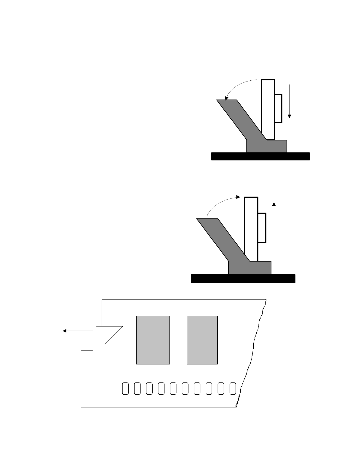
3.1.1 Installing SIMM Modules
1. Insure that power to the system is off.
2. Carefully insert the SIMM module into the socket
at a 90_angle.
3. Slowly rotate the module to lie in the angled
socket. Apply pressure evenly, along the entire
length of the module.
4. The edges of the SIMM module should "click" as
the latches lock into place.
3.1.2 Removing SIMM Modules
1. Insure that power to the system is off.
2. Pull the latch tabs on both ends of the
socket back, away from the module. The
module will rotate slightly, to a position
free of the latches.
3. Rotate the module to 90.
4. Carefully pull the module out.
Rotate Insert
2. 1.
Rotate Remove
1. 2.
Latch
SIMM
Socket

11
3.2 Changing Memory Configuration
If physical memory is removed or added to the system, BIOS will detect the changes
during the power-on self-test period (POST) after reset. It will report the change and
request that Set-up be run.
Run the BIOS Set-up to configure the memory so that BIOS will correctly account for the
memory change. Running Set-up will eliminate the power-up warning.
3.3 Logical Configurations
Portions of the system memory may be allocated as conventional memory, extended
memory, expanded memory, or shadow memory. Conventional, extended, and expanded
memory are all accessible to programs for their own use. Shadow memory is used
exclusively by BIOS. The mix of conventional, extended, expanded, and shadow memory
is dictated primarily by the operating system and programs which will run on the NPC-
486E.
3.2.1 Conventional Memory
Conventional memory is the first 640K bytes of RAM. This memory block is used
extensively by various operating systems and programs common on the PC/AT.
3.2.2 Expanded Memory
Expanded memory refers to a design which allows access to a large address space (e.g.
32M bytes) on a processor such as the 8088, that has address lines to directly address only
1M byte of memory. 16K or 64K sections of memory, called pages, can be "switched"
into addressable blocks (holes) in the expanded memory range. Programs must use the
BIOS extension known as LIM (Lotus/Intel/Microsoft) Expanded Memory Services to
control the switching of pages.
3.2.3 Extended Memory
This is memory beyond the first 1 MB. This memory is directly addressable by programs
in the NPC-486E. However, it is usually controlled by an installed memory manager, such
as HIMEM.SYS, to prevent programs from using the same area of extended memory.

12
3.2.4 Shadow Memory
BIOS may be copied from its ROM memory to a bank of RAM. Execution of BIOS can
then take place from the faster RAM memory, enhancing performance. The RAM used is
called shadow RAM.
A special BIOS utility will copy ROM BIOS to shadow RAM if some of the system
memory is allocated for the shadow RAM (using Set-up).

13
4. IDE Host Adapter
The NPC-486E contains a built-in IDE Host Adapter capable of driving two embedded
hard disks. The embedded drives are connected, in a daisy chain fashion, to the NPC-
486E through a 44 conductor cable.
4.1 Connector
The IDE connector, J11, is a 44-pin, dual-in-line, 2mm, male header.
One or two IDE drives may be connected to the header via a single cable. The first drive
must be configured as the master; the second drive (at the end of the cable) must be
configured as the slave. Consult the disk drive manual for instructions in this task.
The 44-pin, 2mm connector is pin compatible with 2.5" and 1.8" form factor drives.
Power is provided on the cable. An adapter board or cable to convert from the 44-pin,
2mm connector to a 40-pin, 0.1" connector is required to connect to 3.5" hard disk drives.
E27
E28
E18
J1
1
1
J19 U7
U6
E9 U13
2
J2 J3
E5
U8 E8
E7
E6
2
J4 16
E16
E10
E14
E13
E11
E15
E12
U9
E17 U14
1
E1
J18
1
E3
E2
E4 3
E19
E20
E21
E22
E23
E24
E25
U15
U16
U10
E26
U11
J11
IDE
1
J6
J7 J8
J5
1
1
J9
J10
U24
E29
BT1
E30 1
U18
J12
1
1
E31
E32
U21 T1
J17 1
J14J13
1
J16 1
Table of contents


