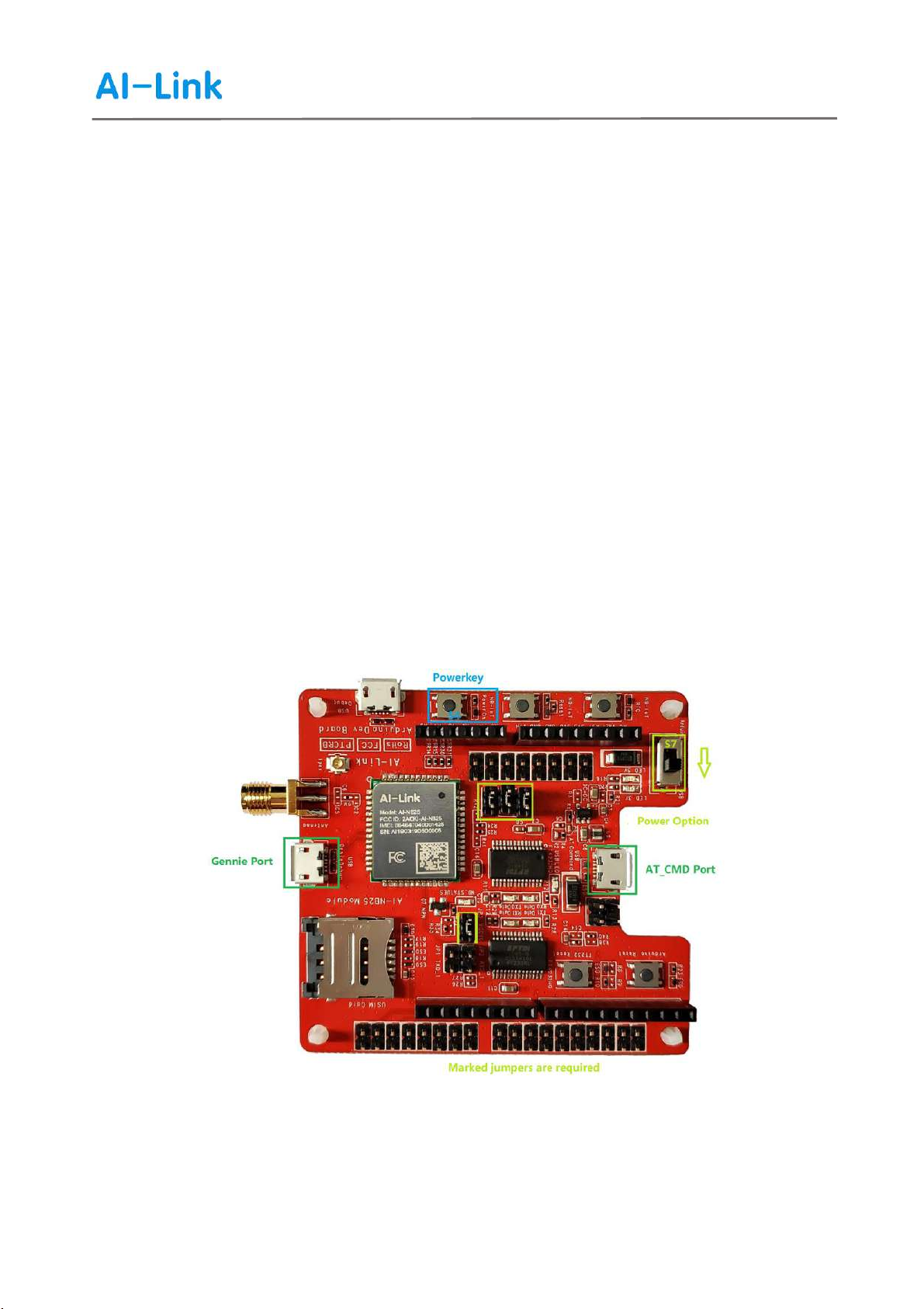
AI-Link AI-NB25-EVB User manual

AI-NB25 Development Kit
Manual
Version: V1.0
Release date: 8 December 2019
AI-Link Confidential
Page 1 of 17

AI-NB25 Development Kit
Manual
Index
1.
INTRODUCTION...............................................................................................................................................3
1.1 Safety Instructions ................................................................................................................................................. 3
2.
OVERVIEW ................................................................................................................................................4
2.1 Performance Summary ........................................................................................................................................ 4
2.2 Functional Block Diagram .................................................................................................................................... 5
2.3 Interface Distribution Diagram ............................................................................................................................. 6
2.4 Arduino Interface Definition Diagram ................................................................................................................... 7
3.
OPERATION INSTRUCTIONS .................................................................................................................8
3.1 Single Board Operation Instructions ................................................................................................................... 8
3.1.1 Schematic Diagram of Single Board ...................................................................................................... 8
3.1.2 Process of Operation .............................................................................................................................. 9
3.2. Multi Board Operation Instructions ...................................................................................................................... 9
3.2.1 Interface and Modification Diagram ...................................................................................................... 10
3.2.2 Process of Operation ............................................................................................................................ 11
3.2.3 Description of I/O Interface Connection ............................................................................................... 11
4.
ELECTRICAL AND RELIABILITY ....................................................................................................... 13
4.1. Absolute Maximum ................................................................................................................................... 13
4.2. Operating and Storage Temperature ....................................................................................................... 13
5.
MECHANICAL DIMENSION .............................................................................................................. 14
5.1. AI-NB25-EVB Mechanical Size ................................................................................................................ 14
5.2. AI-NB25-EVB Top and Bottom View ........................................................................................................ 14
6.
AI-NB25-EVB KIT AND ACCESSORIES ............................................................................................ 15
6.1. AI-NB25-EVB Kit ....................................................................................................................................... 15
6.2. AI-NB25-EVB Accessories ........................................................................................................................ 16
7.
APPENDIX A REFERENCE DOCUMENTS ....................................................................................... 17
Page 2 of 17

AI-NB25 Development Kit
Manual
AI-Link Confidential
1. Introduction
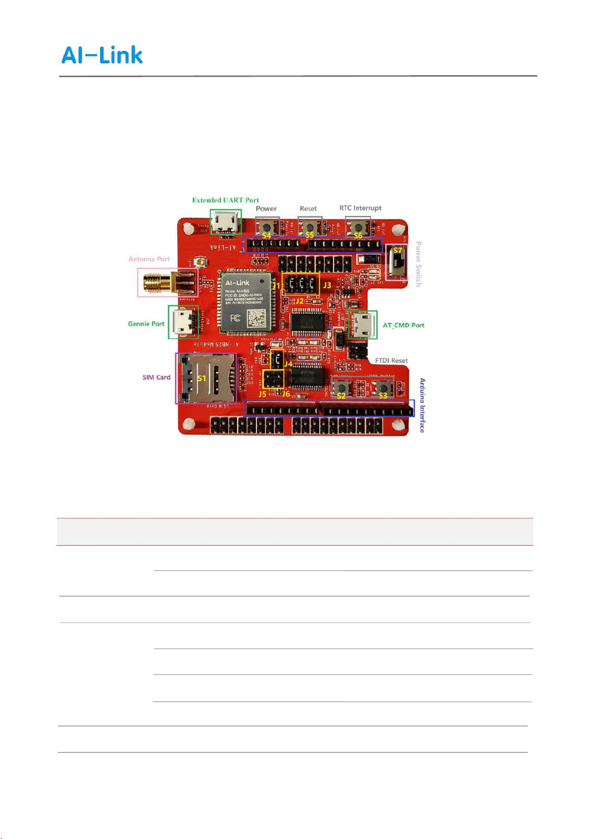
This document defines the AI-NB25-EVB development board and its air interface and hardware
interface connected with customer applications.
This document can help customers quickly understand AI-NB25-EVB development board hardware
interface specifications, electrical characteristics, mechanical specifications and other relevant information
Interest. With the help of this document, combined with our hardware design manual and reference
design manual, customers can quickly apply AI-NB25 module to wireless M2M application.
1.1. Safety instructions
By following the below safety principles, personal safety can be ensured and help to protect the
product and working environment from potential damage.
Road safety first! When you are driving, do not use the hand-held mobile terminal device,
even if it hashands-free function. Please stop and then to call!
Please turn off the mobile terminal before boarding. The wireless function of the mobile
terminal shall not be opened on the aircraft to prevent the opposite flight,
Interference of the communication system of the unit. Ignoring this prompt may lead
to flight safety and even violate the law.
When in hospital or health care place, please pay attention to whether there are restrictions
on the use of mobile terminal equipment. RF interference possible, it may cause medical
devices to run abnormally, so it may be necessary to turn off the mobile terminal device.
The mobile terminal device does not guarantee effective connection under any circumstances,
for example, the mobile terminal device does not any charge or SIM card is invalid.
When you meet the above situations in an emergency, please remember to use the emergency
call, Ensure that your device is powered on and in an area with sufficient signal strength.
Please keep the mobile terminal equipment away from flammable gas. When near gas
stations, oil depots, chemical plants or explosive workplaces, please turn off the mobile
terminal device. Operating electronic equipment in any place with potential explosion
hazard has potential safety hazards.
Page 3 of 17

AI-NB25 Development Kit
Manual
AI-Link Confidential
2. Overview
AI-NB25-EVB is a NB-IoT series development board with standard Arduino interface. Its physical
dimension is 70mm × 66xmm ×11mm. AI-NB25-EVB development board can be used alone or in
combination with STM32 Nucleo-64 series development board for debugging and application
development. Establish communication between NB-IoT radio communication protocol
(3GPP rel. 13 and 3GPP rel. 14) and basic equipment of mobile network operator’s application.
2.1. Performance Summary
The following table details the main performance of AI-NB25-EVB development board.
Table 1:AI-NB25-EVB main performance of development board
Characteristic Explanation
USB Interface
Input voltage range:4.75V~5.25V
Voltage Supply Typical supply voltage:5.0V
Support standard Arduino interface
Transmitting Power 23dBm±2dB
1) Common operating temperature:-35°C ~ +75°C
Temperature Range 2) Extended operating temperature: -40°C ~ +85°C
Storage temperature range:-40°C ~ +90°C
USIM Interface Support 1.8V/3.0V external USIM card
Communication port switch Used to switch Arduino and External USB interface
Provide 3-way UART interface
Main serial port ( AT_CMD port ):
⚫ AT command transmission. The baud rate only support 115200bps
⚫Firmware upgrade. The baud rate only support 921600bps
USB Interface Debug serial port ( Gennie port ):
⚫ Used to output log information for software debugging
⚫ The baud rate only support 921600bps
Auxiliary serial port ( Extended UART port ):
⚫ AT command transfer and data transfer
⚫ The baud rate support 115200bps
Page 4 of 17

AI-NB25 Development Kit
Manual
AI-Link Confidential
Arduino Interface Connected to STM32 Nucleo-64 series development board
Reset button Resetting AI-NB25 module, Low voltage active
Power button Power on AI-NB25 module, Low voltage active
Physical dimension Size: (70.0±0.15) mm × (66.5±0.15) mm × (11±0.2) mm
Firmware upgrade Upgrade through the module's AT serial port or D-Fota/Fota
Antenna interface 50Ωcharacteristic impedance
Remark:
1) 1)Indicates that when the module works in this temperature range, the relevant performance of the
module meets the requirements of 3GPP standard.
2) 2)indicates that when the module works in this temperature range, the module can still maintain normal
working status, with SMS *, data transmission and other functions; There will be unrecoverable failures;
the RF spectrum and network will not be affected basically. Only the values of individual parameters such
as output power may beyond 3GPP standard. When the temperature returns to the normal operating
temperature range, the indicators of the module still meet the 3GPP standard.
2.2. Functional Block Diagram
The figure below is AI-NB25-EVB functional block diagram.
Figure 1:AI-NB25-EVB schematic diagram
Page 5 of 17

AI-NB25 Development Kit
Manual
AI-Link Confidential
2.3. Interface distribution diagram
The following is the interface distribution diagram of AI-NB25-EVB.
Figure 2:AI-NB25-EVB interface distribution
Table 2: list of interfaces
Type Location Description
Power Input I/O AT_CMD Port USB power supply interface
Arduino Interface Arduino power supply interface
USB interface J1 J2 J3 J4 J5 J6 Support 3 groups serial ports
Jumpers Option J1: Gennie port, J2/J3: AT_CMD port, J4/J5/J6: Extended UART port
AT_CMD Port Main serial port, for AT command transmission
Gennie Port NB-IoT Debug Port for GKI/HST logs
Extended UART Port Auxiliary serial port, for communications with extended MCU
USIM interface S1 Micro (U)SIM socket
Page 6 of 17

AI-NB25 Development Kit
Manual
AI-Link Confidential
Arduino interface Arduino I/O Standard Arduino interface
Power Switch S7 Power supply switch between Arduino and USB port
RF interface Antenna Port Radio frequency SMA connector
Power button S4 NB-IoT module power on/off
Reset button S5 NB-IoT module resetting
RTC wake up button S6 NB-IoT wake up from deep sleep mode (PSM)
FTDI Serial Reset S2 S3 FTDI chipset reset function
FTDI Indicator D1 D2 D6 D7 Serial data transmission indicator
Power indicator D3 Power indicator of development kit
2.4. Arduino Interface Definition Overview
The following is the Arduino interface diagram of AI-NB25-EVB.
Figure 3:AI-NB25-EVB interface distribution
Page 7 of 17

AI-NB25 Development Kit
Manual
AI-Link Confidential
3.Operation Instructions
This chapter mainly introduces the specific operation method and process of AI-NB25-EVB,
AI-NB25-EVB can be used for single board and AI-NB25 module firmware upgrade or develop and
debug the Internet of things application based on AI-NB25 module; at the same time, use Arduino
interface with STM32 Nucleo-64 Series development board is used to develop Internet of things
applications based on STM32. The following chapters will introduce the operation process of single
board and multi board respectively.
3.1. Single Board Operation Instructions
This chapter mainly introduces the interface diagram and operation flow when using AI-NB25-EVB alone
3.1.1. Single board operation diagram
Figure 4: Single board operation diagram
Page 8 of 17

AI-NB25 Development Kit
Manual
AI-Link Confidential
3.1.2. Process of Operation
1. Download and install the FTDI (usb-uart) chip driver
The driver is provided by Ai-link technical support team and contact window is: jiaxin.li@changhong.com;
2. Insert micro USIM card into S1 card holder (Sim card need support NB-IoT mode);
3. Connect SMA connector rod antenna on RF connector (Antenna Port);
4. Turn the power option S7 to the " USB " position as above figue3;
5. Use the micro USB data cable to connect the AT_CMD Port (USB port) and the computer,
and then you can see from the "device manager" of the computer that the serial port shown in the
figure below. Then the main serial port of AI-NB25 module is available, which can be used for
at command transmission, Data transmission and firmware upgrade can be applicable to this port ,
you can also use the gennie port for module software debugging once you want to optimate the
firmware with gennie tools (The function major utilized on openCPU solution).
Remark
S4 can be used to turn on the AI-NB25 module, S5 can be used to reset the AI-NB25 module。
3.2. Multi Board Operation Instructions
In this chapter, the operation process of AI-NB25 and STM32 Nucleo-64 series development board
when they are used together will be described in detail.
Page 9 of 17

AI-NB25 Development Kit
Manual
AI-Link Confidential
3.2.1. Interface and modification diagram
t boa
Figure5: Stack AI-NB25-EVB on Nucleo-64 Board through standard Arduino interface
3.2.2. Process of Operation `
1. Install the STM32 nucleo-64 development board driver.
The download address of the driver is:
https://www.st.com/content/st_com/en/products/evaluation-tools/product-evaluation-tools/mcu-mpu
-eval-tools/stm32-mcu-mpu-eval-tools/stm32-nucleo-boards.html
2. Install the FTDI chip driver.
The driver is provided by Ai-link technical support team and contact window is: jiaxin.li@changhong.com
3. Short the jumpers CN1,CN2,JP5,JP6,JP7,JP8 pin1 and 2 on the front of STM32 nucleo-64
development board before place stack with the AI-NB25-EVB on it.
4. Insert micro USIM card into S1 card holder (Sim card need support NB-IoT mode);
5. Connect SMA connector rod antenna on RF connector (Antenna Port);
6. Turn the power option to the "Arduino" position and set all of the required jumpers;
7. Stack AI-NB25-EVB on nucleo-64 board through standard Arduino interface shown as above figure;
8. Connect the STM32 nucleo-64 development board with the computer through the Mini USB data
cable, and you can also do the same connection between AI-NB25-EVK AT or gennie port with
computer if necessary, then the driver can be shown in the "device manager” of computer.
S1
J10
Page 10 of 17

AI-NB25 Development Kit
Manual
AI-Link Confidential
STM32 nucleo-64 development board need optimized for multi board operation.
Nucleo-64 board top view
Nucleo-64 board bottom view
Page 11 of 17

AI-NB25 Development Kit
Manual
AI-Link Confidential
Table 3:STM32 Series MCU and AI-NB25-EVB Connection
No MCU (STM32) Arduino AI-NB25 Remarks
1PA2 D1 UART0_NB_RX STM32_MCU_TX
2 PA3 D0 UART0_NB_TX STM32_MCU_RX
3 PB5 D4 PSM_EINT_N PSM Interrupt
4 PB10 D6 PWRKEY_N Power On
5 NRST NRST RESET_N Rest NB-IoT
6 PC1/PC0 A4,A5 UART1_NB_RX/TX Auxiliary UART Ports
7 +5V +5V +5V Input 5.0V Power Supply
8 GND GND Ground Ground
9 A0,A1,A2,A3 A0,A1,A2,A3 GPIO0/1/3/9 Reserved GPIOs
10 D10~D15 D10~D15 GPIO12/13/14/15/6/7 Reserved GPIOs
11 D7,D5,D3,D2 D7,D5,D3,D2 GPIO28/18/30/8 Reserved GPIOs
The following is the schematic diagram of STM32 MCU and AI-NB25 pin connection。
Page 12 of 17

AI-NB25 Development Kit
Manual
AI-Link Confidential
4.Electrical Performance and Reliability
4.1. Absolute maximum
The table below shows the maximum withstand value of power supply voltage and current of digital and
analog pins of AI-NB25 module.
Table 4:Absolute maximum
Parameter Min Max Unit
+5V -0.3 6 V
VBAT TBD TBD V
Power supply current TBD TBD A
Digital pin voltage TBD TBD V
Analog pin voltage TBD TBD V
Digital / analog pin voltage in power off mode TBD TBD V
4.2. Operating and storage temperature
The following table shows the operating and storage temperature ranges of the AI-NB25 module。
Table 5:Module operating and storage temperature range
Parameter Min Typic Max Unit
Normal operating temperature range 1) -35 +25 +75 ºC
Extended operating temperature range 2) -40 +85 ºC
Storage temperature range -40 +90 ºC
Page 13 of 17

AI-NB25 Development Kit
Manual
AI-Link Confidential
Remark
1. 1)Indicates that when the module works in this temperature range, the relevant performance of the module
meets the requirements of 3GPP standard;
2. 2)It means that when the module works in this temperature range, the module can still maintain normal
working status, with SMS *, data transmission and other functions, no There will be unrecoverable failures.
The radio frequency spectrum and network are basically unaffected. Only the values of some parameters
such as output power may beyond 3GPP standard. When the temperature returns to the normal
operating temperature range, the indicators of the module still meet the 3GPP standard.
5.Mechanical Dimension
This chapter describes the mechanical dimensions of AI-NB25-EVB. Dimensions are in mm with a tolerance of ± 0.15mm.
5.1. AI-NB25-EVB Mechanical Dimension
Figure6: AI-NB25-EVB Dimension (Unit: mm)
Page 14 of 17

AI-NB25 Development Kit
Manual
AI-Link Confidential
6.AI-NB25-EVB Board and Accessories
6.1. AI-NB25-EVB Development Kit
AI-NB25-EVB single board operation diagram:
Comments: AI-NB25-EVB single board operated schematic without ST32 nucleo-64 board.
Page 15 of 17

AI-NB25 Development Kit
Manual
AI-Link Confidential
6.2. AI-NB25-EVB Accessories
Packing form of AI-NB25-EVB as following for overview:
Table 6:Accessories list
Accessories Describe Quantity
Antenna Rod NB-IOT antenna with SMA connector 1
Signal data cable Micro USB cable 2
Instructions Single page instruction for EVB accessories 1
AI-NB25-EVBDevelopment kit of AI-NB25 Module 1
Page 16 of 17

AI-NB25 Development Kit
Manual
AI-Link Confidential
7. Appendix a Reference Documents
Table 7:Reference document
No. Document Name Comments
[1] AI-NB25 Specification User manual AI-NB25 User Manual
Table 8: terms and abbreviations
Abbreviation Describe
DFOTA Differential firmware upgrade over-the-air
MCU Microcontroller unit
NB-IoT Narrow band internet of things
SMA Small A Type connector
UART Universal asynchronous receiver & transmitter
USB Universal serial bus
Page 17 of 17
This manual suits for next models
1
Table of contents