aion CYGNUS User manual

CYGNUS DISTORTION/SUSTAINER 1
PROJECT NAME
CYGNUS
BASED ON
EFFECT TYPE
PROJECT SUMMARY
DOCUMENT VERSION
Cornish P-2 / G-2
Based on the classic Big Muff circuit, this pedal adds a meticulously-designed buffered bypass along with
an additional transistor-based buffer stage on the effect input.
Distortion / sustainer, fuzz 2.0.0 (2023-10-06)
Actual size is 2.3” x 2.43” (main board) and 2.3” x 0.87” (bypass board).
BUILD DIFFICULTY
Intermediate

CYGNUS DISTORTION/SUSTAINER 2
TABLE OF CONTENTS
1Project Overview 10 Drill Template
2Introduction & Usage 11 Enclosure Layout
3-5 Parts List 12 Wiring Diagram
6-7 Build Notes 13 Licensing
8Schematic (P-2) 13 Document Revisions
9Schematic (G-2)
INTRODUCTION
The Cygnus Distortion/Sustainer is adapted from the Pete Cornish P-2 and G-2, two Big Muff-based
pedals that share a PCB but with several part differences to distinguish them.
Cornish pedals are probably best known for being extremely expensive. There are two reasons for this.
First, the build quality and reliability is unmatched. Second, the mysterious nature of them, partially
due to the fact that the circuit is obscured and partially because of the A-list of clients. (The P-2 was
originally designed for David Gilmour, while the G-2 was developed with Lou Reed.)
Inside, the circuit is a basic Big Muff with a few changes such as a simplified hi-cut tone control and
the famous class-A transistor buffer design. The P-2 is similar to a Ram’s Head Muff, while the G-2 was
designed to be much lower gain with a drastically different EQ as well as germanium clipping diodes. In
fact, until the G-2 it was traced in 2009, people had no idea it was a Muff derivative. The P-2 was traced
by Aion FX in 2023.
The Cygnus is a faithful reproduction of the G-2 and P-2 circuits, and the parts list includes both
variants. The default is the P-2 circuit, while each G-2 change is listed in the “Notes” column.
We’ve made one major addition in our project: an internal switch allowing the pedal to be used in true-
bypass mode instead of buffered bypass. As with the Klon KTR, the buffer mode is “almost always
better”, but you can be the judge of that.
USAGE
The Cygnus has the following controls:
• Sustain controls the signal level going into the first clipping stage, which affects the amount of drive
or sustain.
• Tone is a basic high-cut filter.
• Volume is the overall output.

CYGNUS DISTORTION/SUSTAINER 3
PARTS LIST
This parts list is also available in a spreadsheet format which can be imported directly into Mouser for
easy parts ordering. Mouser doesn’t carry all the parts (most notably potentiometers) so the second tab
lists all the non-Mouser parts as well as sources for each.
View parts list spreadsheet →
PART VALUE TYPE NOTES
R1 10M Metal film resistor, 1/4W
R2 1k Metal film resistor, 1/4W
R3 120k Metal film resistor, 1/4W
R4 120k Metal film resistor, 1/4W
R5 200k Metal film resistor, 1/4W
R6 7k5 Metal film resistor, 1/4W
R7 10k Metal film resistor, 1/4W
R8 51R Metal film resistor, 1/4W
R9 1M Metal film resistor, 1/4W
R10 1k Metal film resistor, 1/4W
R11 120k Metal film resistor, 1/4W
R12 68k Metal film resistor, 1/4W
R13 150k Metal film resistor, 1/4W
R14 10k Metal film resistor, 1/4W G-2 uses 8k2.
R15 39k Metal film resistor, 1/4W
R16 100k Metal film resistor, 1/4W
R17 470k Metal film resistor, 1/4W
R18 15k Metal film resistor, 1/4W G-2 value is likely 15k, but 18k is recommended. See build notes.
R19 100R Metal film resistor, 1/4W G-2 value is likely 680R, but 100R is recommended. See build notes.
R20 100R Metal film resistor, 1/4W G-2 uses 1k.
R21 8k2 Metal film resistor, 1/4W
R22 100k Metal film resistor, 1/4W
R23 470k Metal film resistor, 1/4W
R24 15k Metal film resistor, 1/4W
R25 100R Metal film resistor, 1/4W G-2 uses 680R.
R26 8k2 Metal film resistor, 1/4W
R27 100k Metal film resistor, 1/4W
R28 470k Metal film resistor, 1/4W
R29 15k Metal film resistor, 1/4W
R30 100R Metal film resistor, 1/4W
R31 100k Metal film resistor, 1/4W
R32 390k Metal film resistor, 1/4W

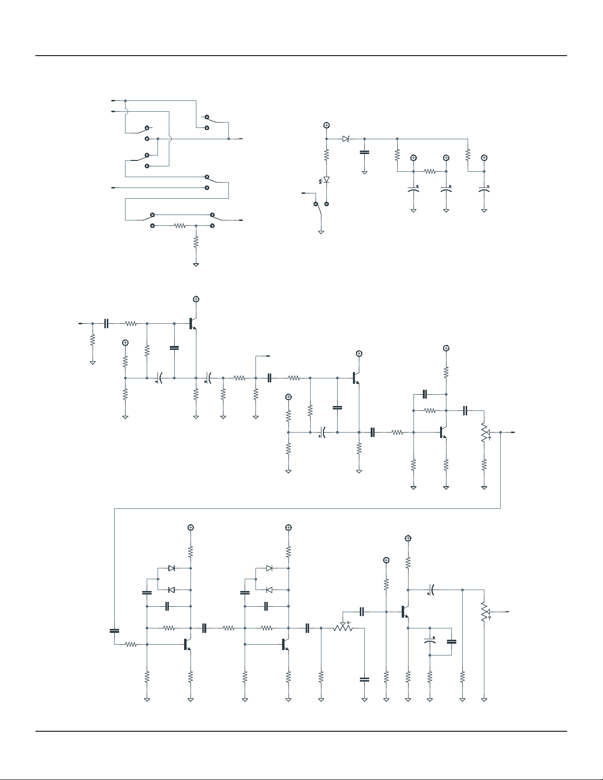
CYGNUS DISTORTION/SUSTAINER 4
PARTS LIST, CONT.
PART VALUE TYPE NOTES
R33 100k Metal film resistor, 1/4W
R34 10k Metal film resistor, 1/4W G-2 uses 8k2.
R35 2k2 Metal film resistor, 1/4W
R36 1k2 Metal film resistor, 1/4W G-2 uses 620R.
R37 39k Metal film resistor, 1/4W
R38 91R Metal film resistor, 1/4W
R39 51k Metal film resistor, 1/4W
R40 100R Metal film resistor, 1/4W
R41 120R Metal film resistor, 1/4W
R42 100R Metal film resistor, 1/4W
LEDR 10k Metal film resistor, 1/4W LED current-limiting resistor. Adjust value to change LED brightness.
C1 100n Film capacitor, 7.2 x 2.5mm
C2 4.7uF Electrolytic capacitor, 4mm
C3 1n Film capacitor, 7.2 x 2.5mm
C4 22uF Electrolytic capacitor, 5mm
C5 220n Film capacitor, 7.2 x 2.5mm
C6 4.7uF Electrolytic capacitor, 4mm
C7 10n Film capacitor, 7.2 x 2.5mm
C8 47n Film capacitor, 7.2 x 2.5mm
C9 470pF MLCC capacitor, NP0/C0G G-2 uses 1n film.
C10 47n Film capacitor, 7.2 x 2.5mm
C11 47n Film capacitor, 7.2 x 2.5mm
C12 470pF MLCC capacitor, NP0/C0G G-2 uses 1n film.
C13 220n Film capacitor, 7.2 x 2.5mm
C14 2.2uF Film capacitor, 7.2 x 5mm
C15 470pF MLCC capacitor, NP0/C0G G-2 uses 1n film.
C16 220n Film capacitor, 7.2 x 2.5mm
C17 2.2uF Film capacitor, 7.2 x 5mm
C18 10n Film capacitor, 7.2 x 2.5mm
C19 220n Film capacitor, 7.2 x 2.5mm
C20 OMIT Electrolytic capacitor, 5mm G-2 uses 22uF. Omit (leave empty) for P-2.
C21 22uF Electrolytic capacitor, 5mm
C22 100n MLCC capacitor, X7R Power supply filter capacitor.
C23 220uF Electrolytic capacitor, 6.3mm Power supply filter capacitor.
C24 100uF Electrolytic capacitor, 6.3mm Power supply filter capacitor.
C25 220uF Electrolytic capacitor, 6.3mm Power supply filter capacitor.
C26 10n Film capacitor, 7.2 x 2.5mm P-2 only. Omit (leave empty) for G-2.

CYGNUS DISTORTION/SUSTAINER 5
PARTS LIST, CONT.
PART VALUE TYPE NOTES
D1 1N5817 Schottky diode, DO-41
D2 1N914 Fast-switching diode, DO-35 G-2 uses germanium (e.g. 1N34A).
D3 1N914 Fast-switching diode, DO-35 G-2 uses germanium (e.g. 1N34A).
D4 1N914 Fast-switching diode, DO-35 G-2 uses germanium (e.g. 1N34A).
D5 1N914 Fast-switching diode, DO-35 G-2 uses germanium (e.g. 1N34A).
Q1 BC550C BJT transistor, NPN, TO-92 G-2 uses BC549C.
Q2 BC550C BJT transistor, NPN, TO-92 G-2 uses BC549C.
Q3 BC550C BJT transistor, NPN, TO-92 G-2 uses BC549C.
Q4 BC550C BJT transistor, NPN, TO-92 G-2 uses BC549C.
Q5 BC550C BJT transistor, NPN, TO-92 G-2 uses BC549C.
Q6 BC550C BJT transistor, NPN, TO-92 G-2 uses BC549C.
SUSTAIN 100kA 16mm right-angle PCB mount pot G-2 uses 50kA.
TONE 25kB 16mm right-angle PCB mount pot
VOLUME 10kA 16mm right-angle PCB mount pot
TB-BUF 4PDT slide Slide switch, 4PDT E-Switch EG4208 (4mm lever) or EG4208A (6mm lever)
IN 1/4" mono 1/4" phone jack, closed frame Switchcraft 111X or equivalent.
OUT 1/4" mono 1/4" phone jack, closed frame Switchcraft 111X or equivalent.
DC 2.1mm DC jack, 2.1mm panel mount Mouser 163-4302-E or equivalent.
FSW 3PDT Stomp switch, 3PDT
ENC 125B Enclosure, die-cast aluminum Can also use a Hammond 1590N1.

CYGNUS DISTORTION/SUSTAINER 6
BUILD NOTES
Bypassing the true bypass / buffer switch
The E-Switch EG4208 slide switch used for the true bypass/buffer selector is available from Mouser
Electronics but may not be accessible to everyone. If you are unable to obtain it, you can hard-wire the
switch to either true bypass mode or buffered mode by soldering jumpers to the switch pads.
C14 and C17 capacitors
In both the P-2 and G-2, the coupling capacitors immediately after Q4 and Q5 (C14 and C17) are 4.7uF
electrolytics. Since film capacitors are generally viewed as superior to electrolytic within the audio path,
we used a film capacitor footprint. However, 4.7uF film capacitors are unnecessarily expensive and
large, so we reduced the recommended value to 2.2uF.
There will be no audible difference between 4.7uF and 2.2uF since the output impedance coming off the
transistors is low. Most likely you could go down to 1uF or even further with no change.
If you do want to use electrolytics in these two positions instead, the polarity has been marked on the
PCB. (Film caps have no polarity, so this marking can be ignored if using the recommended caps.)
R7 and R39 resistor values (G-2 only)
The original G-2 trace from 2009 showed a 50k resistor for the output pulldown resistor (R39 in this
project, R40 in the original trace schematic).
This may have been correct for the unit that was traced, but 50k is a non-standard resistor value, and
each of the seven Cornish pedals we’ve traced has used 51k here. So whether or not it’s an error, we’re
pretty confident that current-production G-2 units would use 51k.
This makes no practical difference to the finished pedal, only changing the output impedance by around
2%, but we’re meticulous!
In addition, R7 (R10 in trace) was shown as a 20k resistor in the original trace. It’s possible this was
correct in that particular G-2 unit, but once again, each of the seven that we’ve traced has used 10k here.
Since the buffer is a separate PCB module shared between all of the pedals, we’re confident that the
current-production G-2 uses 10k as well.
BUFFER BYPASS
TRUE BYPASS

CYGNUS DISTORTION/SUSTAINER 7
BUILD NOTES, CONT.
Resistors & diodes in the first clipping stage (G-2 only)
The G-2 was first traced in 2009 by Dirk Hendrik for freestompboxes.org. The trace was thorough, and
other than the resistors mentioned above, there is no reason to doubt its accuracy.
However, with thousands of people building clones based on the schematic in the years since, it’s
become apparent that the choice of diodes in the first gain stage is very important. The G-2 uses
germanium diodes, which are notoriously inexact and have a wide variance in forward voltage even
among the same part number. Germanium diodes usually have forward voltages from 0.2V to 0.4V, with
some types going even higher or lower.
If the diodes have too low of a forward voltage, the transistor’s gain is not high enough to keep up and as
a result it will not distort the signal like it should. There are three solutions to this potential issue:
1. Use germanium diodes with a forward voltage above ~0.3V. (No testing has been done to see where
the cutoff is, so you might be able to go slightly lower or you may need to go even higher.)
2. Use BAT41 diodes (silicon Schottky) instead of germanium. These have a forward voltage of around
0.4V which is more than enough.
3. Increase the gain of the previous stage by using an 18k resistor for R18 and 100R for R19.
Since #3 is the simplest and most universal solution, the parts list for the G-2 variant has been updated
to use these values by default. If you’d like to try #1 or #2, though, you should use the original Cornish
values of 15k for R18 and 680R for R19.
The P-2 does not have this issue since it uses silicon clipping diodes and has higher gain throughout.
Tone modifications (G-2 only)
The G-2 is known for having significantly more low-end than a standard Big Muff circuit, and this can
sometimes be too much in a live setting depending on the mix.
If you want to keep most of the G-2’s character but cut the bass, try omitting C20 (the G-2’s 22uF
capacitor in the last stage) and instead using C26 (the P-2’s 10n capacitor). This is responsible for a lot of
the bass-heaviness, and that single change will go a long way. It’s also recommended to reduce the input
capacitor (C1) to 100n.
Transistor substitutions
The BC549C (G-2) and BC550C (P-2) are interchangeable with no difference in sound, so either can be
used. If you want to substitute a different transistor, you’ll want one with very high hFE, in the 600s.
The PCB layout uses the B-C-E transistor pinout, which is the opposite of the E-B-C convention used by
transistors with a “2N” prefix such as the 2N3904. The closest substitute in this series is the 2N5089. If
using these, rotate them 180 degrees. Use a multimeter to check the pinout if you’re not sure.
The transistor outlines also include a rectangular collector pad above the “B” and “E” pins so that a SMD
transistor such as the BC849C can be used.

CYGNUS DISTORTION/SUSTAINER 8
SCHEMATIC (P-2)
TO PCB IN
BUFFER OUT
TO INPUT JACK
TO OUTPUT JACK
FROM BUFFER OUT
FROM EFFECT OUT
SWITCH POSITIONS SHOWN
Slide switch: TBP mode
Footswitch: bypass mode
FX GND
EFFECT OUT
PCB IN
FX GND
10k
5MM
1N5817
220uF
GND
+9V
100n
VA
GND GND GND
GNDGND GND GNDGND GNDGND
39k
100k
470k
100R 15k
100R
8k2
100k
470k
100R 15k
8k2
100k
470k
100R 15k
390k100k
10k2k2
47n
470pF
47n
47n
470pF
220n
470pF
220n
220n
BC550C
BC550C BC550C
BC550C
100kA10kA
1N914
1N914
1N914
1N914
39k
GND
1k2
GND
22uF
25kB
10n
GND
100k
GND
100R
120R
100R
100uF 220uF
GND GND
VC
91R
51k
VD VD
VD
VD
VC
10M
100n
1k
120k
120k200k
1n
4.7uF
BC550C
7k5
22uF
10k
51R
GND GND GND
GND
1M
220n
1k
120k
68k150k
10n
4.7uF
BC550C
10k
GND GND
GND
VC
VC
GND
2.2uF
2.2uF
VA
VA
VD
10n
OMIT
GND
GND
LEDR
LED
D1
C23
A2
A3
A1 FSA
B2
B3
B1
FSB
C2
C3
C1 FSC
C22
R15
R16
R17
R19 R18
R20
R21
R22
R23
R25 R24
R26
R27
R28
R30 R29
R32R33
R34R35
C8
C9
C10
C11
C12
C13
C15
C16
C19
Q3
Q4 Q5
Q6
SUSTAIN
1
2
3
VOLUME
1
2
3
D2
D3
D4
D5
R37
R36 C21
TONE
1
2
3
C18
R31
R40
R41
R42
C24 C25
SW1A
2
3
1
SW1B
5
6
4
SW1C
8
9
7
SW1D
11
12
10
R38
R39
R1
C1
R2
R3
R4R5
C3
C2
Q1
R6
C4
R7
R8
R9
C5
R10
R11
R12R13
C7
C6
Q2
R14
C14
C17
C26
C20

CYGNUS DISTORTION/SUSTAINER 9
SCHEMATIC (G-2)
TO PCB IN
BUFFER OUT
TO INPUT JACK
TO OUTPUT JACK
FROM BUFFER OUT
FROM EFFECT OUT
SWITCH POSITIONS SHOWN
Slide switch: TBP mode
Footswitch: bypass mode
FX GND
EFFECT OUT
PCB IN
FX GND
10k
5MM
1N5817
220uF
GND
+9V
100n
VA
GND GND GND
GNDGND GND GNDGND GNDGND
39k
100k
470k
100R 18k
1k
8k2
100k
470k
680R 15k
8k2
100k
470k
100R 15k
390k100k
8k22k2
47n
1n
47n
47n
1n
220n
1n
220n
220n
BC549C
BC549C BC549C
BC549C
50kA10kA
Ge
Ge
Ge
Ge
39k
GND
620R
GND
22uF
25kB
10n
GND
100k
GND
100R
120R
100R
100uF 220uF
GND GND
VC
91R
51k
VD VD
VD
VD
VC
10M
100n
1k
120k
120k200k
1n
4.7uF
BC549C
7k5
22uF
10k
51R
GND GND GND
GND
1M
220n
1k
120k
68k150k
10n
4.7uF
BC549C
8k2
GND GND
GND
VC
VC
GND
2.2uF
2.2uF
VA
VA
VD
OMIT
22uF
GND
GND
LEDR
LED
D1
C23
A2
A3
A1 FSA
B2
B3
B1
FSB
C2
C3
C1 FSC
C22
R15
R16
R17
R19 R18
R20
R21
R22
R23
R25 R24
R26
R27
R28
R30 R29
R32R33
R34R35
C8
C9
C10
C11
C12
C13
C15
C16
C19
Q3
Q4 Q5
Q6
SUSTAIN
1
2
3
VOLUME
1
2
3
D2
D3
D4
D5
R37
R36 C21
TONE
1
2
3
C18
R31
R40
R41
R42
C24 C25
SW1A
2
3
1
SW1B
5
6
4
SW1C
8
9
7
SW1D
11
12
10
R38
R39
R1
C1
R2
R3
R4R5
C3
C2
Q1
R6
C4
R7
R8
R9
C5
R10
R11
R12R13
C7
C6
Q2
R14
C14
C17
C26
C20

CYGNUS DISTORTION/SUSTAINER 10
DRILL TEMPLATE
Cut out this drill template, fold the edges and tape it to the enclosure. Before drilling, it’s recommended
to first use a center punch for each of the holes to help guide the drill bit.
Ensure that this template is printed at 100% or “Actual Size”. You can double-check this by measuring
the scale on the printed page.
Top jack layout assumes the use of closed-frame jacks like the Switchcraft 111X. If you’d rather use
open-frame jacks, please refer to the Open-Frame Jack Drill Template for the top side.
LED hole drill size assumes the use of a 5mm LED bezel, available from several parts suppliers. Adjust
size accordingly if using something different, such as a 3mm bezel, a plastic bezel, or just a plain LED.
0 1 2
CM
0 1
INCH
ø3/8” ø1/2”
0.385”
0.625” 0.625”
x: 0, y: -1.775
ø15/32”
x: -0.775, y: -1.775
ø5/16”
ø3/8”
125B
OUT
VOLUME SUSTAIN
TONE
FOOTSWITCHLED
DC IN
x: -0.65, y: +1.71 x: 0.65, y: +1.71
ø9/32” ø9/32”
x: 0, y: +0.66
ø9/32”
CENTER (0,0)

CYGNUS DISTORTION/SUSTAINER 11
ENCLOSURE LAYOUT
Enclosure is shown without jacks. See next page for jack layout and wiring.
125B

CYGNUS DISTORTION/SUSTAINER 12
WIRING DIAGRAM
125B
IN +VF.GND GND BUF FX
PCB
IN
FX
GND
+V +V JACK GND JACK
OUTIN
GND BUF
OUT
FX
OUT

CYGNUS DISTORTION/SUSTAINER 13
LICENSE & USAGE
No direct support is offered for these projects beyond the provided documentation. It’s assumed
that you have at least some experience building pedals before starting one of these. Replacements and
refunds cannot be offered unless it can be shown that the circuit or documentation are in error.
All of these circuits have been tested in good faith in their base configurations. However, not all the
modifications or variations have necessarily been tested. These are offered only as suggestions based
on the experience and opinions of others.
Projects may be used for commercial endeavors in any quantity unless specifically noted. No
attribution is necessary, though a link back is always greatly appreciated. The only usage restrictions
are that (1) you cannot resell the PCB as part of a kit without prior arrangement, and (2) you cannot
“goop” the circuit, scratch off the screenprint, or otherwise obfuscate the circuit to disguise its source.
(In other words: you don’t have to go out of your way to advertise the fact that you use these PCBs, but
please don’t go out of your way to hide it. The guitar effects industry needs more transparency, not less!)
DOCUMENT REVISIONS
2.0.0 (2023-10-06)
• New PCB layout to add P-2 compatibility based on our trace.
• Changed transistor outlines to BC549/550 convention.
• Changed R7 from 20k to 10k and added information on this change to the build notes section.
1.0.2 (2023-08-04)
Changed R39 from 50k to 51k and added information on this change to the build notes section.
1.0.1 (2020-04-06)
Added notes about resistors in first transistor stage (R18 and R19).
1.0.0 (2019-03-14)
Initial release.
Table of contents
Other aion Music Equipment manuals

aion
aion ANDROMEDA DELUXE User manual

aion
aion Cinder User manual

aion
aion theseus User manual

aion
aion XIPHOS User manual

aion
aion HELIODOR AMP OVERDRIVE User manual

aion
aion VULCAN User manual

aion
aion Heliosphere User manual

aion
aion MAELSTROM User manual

aion
aion ACHILLES User manual

aion
aion Parhelion User manual