2
Allegro MicroSystems
955 Perimeter Road
Manchester, NH 03103-3353 U.S.A.
www.allegromicro.com
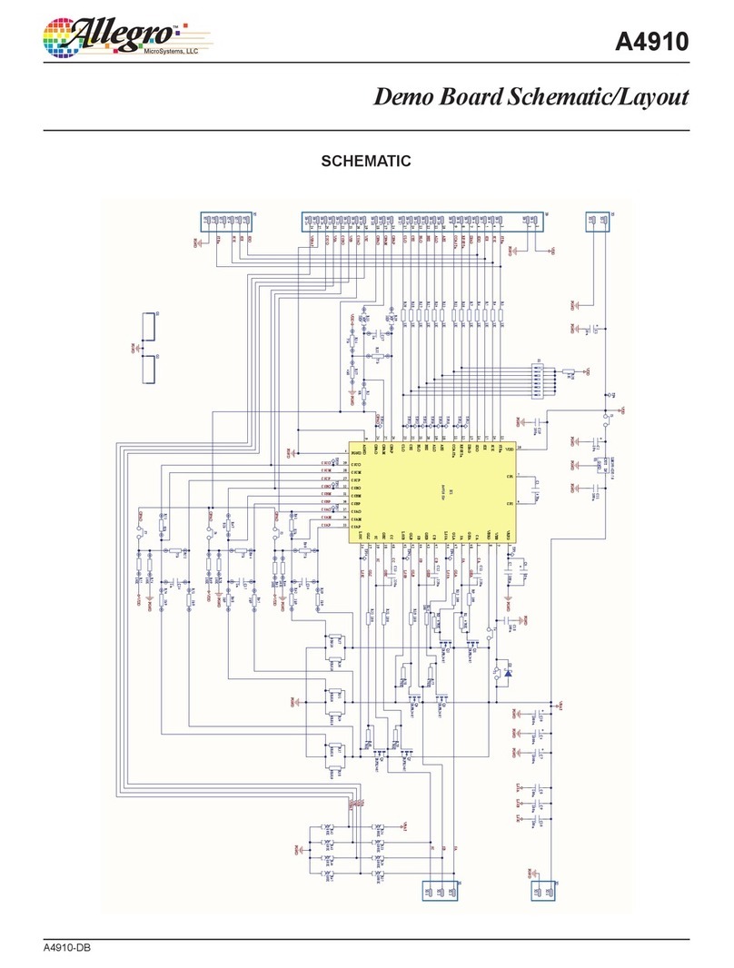
Figure 2: Schematic for ACS732 and ACS733 Demo Board
Table 2: Terminal List Table
Number Name Description
1,2,3,4 IP+ Positive terminals for current being sensed; fused internally.
5,6,7,8 IP– Negative terminals for current being sensed; fused internally.
9,10 GND Device ground terminal.
11 PROGRAM Programming input pin for factory calibration. Connect to ground for
best ESD performance.
12 VIOUT Analog output signal.
13 FAULT Overcurrent Fault output. Open drain.
14 VOC Set the overcurrent fault threshold via external resistor divider on this
pin.
15,16 VCC Device power supply terminal.
Package LA, 16-Pin
SOICW Pinout Diagram
1
2
3
4
5
6
7
8
16
15
14
13
12
11
10
9
IP+
IP+
IP+
IP+
IP–
IP–
IP–
IP–
VCC
VCC
VOC
FAULT
VIOUT
PROGRAM
GND
GND
PINOUT DIAGRAM AND TERMINAL LIST
