AlphaPC 164 User manual

AlphaPC164Motherboard
User’sManual
Revision/Update Information: This is a new manual.

May 1996
Printed in U.S.A.
AlphaPC, Digital, and Digital Semiconductor are trademarks of Digital Equipment Corporation.
CDC is a registered trademark of Control Data Corporation.
CompuServe is a registered trademark of CompuServe, Inc.
FaxBACK and Intel are registered trademarks of Intel Corporation.
GRAFOIL is a registered trademark of Union Carbide Corporation.
Microsoft is a registered trademark and NT and Windows NT are trademarks of Microsoft
Corporation.
QLogic is a registered trademark and ISP is a trademark of QLogic Corporation.
SMC is a registered trademark of Standard Microsystems Corporation.
Standard Microsystems is a registered trademark of Standard Microsystems Corporation.
TriQuint is a registered trademark of TriQuint Semiconductor, Inc.
Xilinx is a trademark of Xilinx, Incorporated.
Digital Semiconductor is a Digital Equipment Corporation business.
All other trademarks and registered trademarks are the property of their respective holders.
EC–QPG0A–TE

Contents
1About This Manual ................................... 1
1.1 Document Conventions . . ........................... 1
2Features of the AlphaPC 164 Motherboard ................. 3
2.1 Power Requirements ............................... 6
2.2 Environmental Requirements ........................ 7
2.3 Physical Parameters ............................... 7
3AlphaPC 164 Jumper Configuration . . . ................... 8
3.1 Memory Bus Width Jumper (J1) . . . ................... 8
3.2 System Clock Divisor Jumpers (IRQ3 through IRQ0) ...... 8
3.3 Bcache Size Jumpers (CF1 and CF2) ................... 8
3.4 Bcache Speed Jumpers (CF4 and CF5) ................. 8
3.5 Mini-Debugger Jumper (CF6) ........................ 10
3.6 Boot Option Jumper (CF7) ........................... 10
3.7 Flash ROM Update Jumper (J31) . . ................... 10
4AlphaPC 164 Connector Pinouts ......................... 11
5Configuring and Upgrading DRAM Memory ................ 19
5.1 Configuring DRAM Memory .......................... 19
5.2 Upgrading DRAM Memory .......................... 20
6Interrupts and ISA Bus Addresses........................ 21
6.1 Interrupts ....................................... 21
6.2 ISA I/O Address Map ............................... 22
6.3 Flash ROM Address Map . ........................... 22
7Windows NT ARC Firmware . ........................... 23
7.1 Firmware Conventions . . . ........................... 23
7.2 Firmware Menu Access . . ........................... 23
7.3 Firmware Menu Structure ........................... 23
7.4 Firmware Menu Descriptions ......................... 25
7.4.1 Boot Menu . ................................... 25
7.4.2 Supplementary Menu . ........................... 26
7.4.3 Setup Menu ................................... 27
7.4.4 Manage Boot Selection Menu . . . ................... 30
7.4.5 Machine Specific Setup Menu . . ................... 32
7.5 Using the Disk Partition Utility....................... 32
iii

7.6 Using the Firmware Update Utility .................... 34
7.7 Installing the Windows NT Operating System ............ 34
7.7.1 Requirements . . ................................ 35
7.7.2 Before Installing Windows NT ..................... 36
7.7.3 Starting Windows NT Setup ...................... 37
8Troubleshooting ...................................... 38
8.1 Beep Codes....................................... 39
8.2 Post Codes ....................................... 39
8.3 Fail-Safe Booter . . . ................................ 41
9Ordering Associated Literature . . ........................ 42
Figures
1AlphaPC 164 Jumper/Connector/Component Location ..... 4
2AlphaPC 164 Configuration Jumpers . . ................ 9
Tables
1AlphaPC 164 Features ............................. 3
2AlphaPC 164 Jumper/Connector/Component List . . ....... 5
3Power Supply dc Current Requirements ................ 6
4AlphaPC 164 Motherboard Environmental Requirements. . . 7
5Peripheral Component Interface (PCI) Bus Connector
Pinouts. . ........................................ 11
6ISA Expansion Bus Connector Pinouts (J33, J35) . . ....... 13
7DRAM SIMM Connector Pinouts (J5 through J12) . ....... 14
8IDE Drive Bus Connector Pinouts (J13, J14) ............. 14
9Diskette Drive Bus Connector Pinouts (J18) ............. 15
10 Parallel Bus Connector Pinouts (J16) . . ................ 15
11 COM1/COM2 Serial Line Connector Pinouts (J4) . . ....... 15
12 Keyboard/Mouse Connector Pinouts (J15) ............... 16
13 SROM Test Data Input Connector Pinouts (J32) . . . ....... 16
14 Input Power Connector Pinouts (J3) . . . ................ 16
15 Enclosure Fan (+12 Vdc) Power Connector Pinouts (J2,
J22) ............................................ 17
16 Speaker Connector Pinouts (J23) ...................... 17
17 Microprocessor Fan Power Connector Pinouts (J21). ....... 17
18 Power LED Connector Pinouts (J27) . . . ................ 17
19 IDE Drive LED Connector Pinouts (J28) ................ 18
iv

20 Reset Button Connector Pinouts (J24) .................. 18
21 Halt Button Connector Pinouts (J25) ................... 18
22 AlphaPC 164 DRAM Memory Configurations . . .......... 19
23 Memory Upgrade Options ........................... 20
24 ISA Interrupts . ................................... 21
25 ISA I/O Address Map ............................... 22
26 Beep Codes....................................... 39
27 Post Codes ....................................... 39
v


1 About This Manual
This manual describes the AlphaPC 164 motherboard, a module for computing
systems based on the Digital Semiconductor 21164 Alpha microprocessor and
the companion Digital Semiconductor 21172 core logic chipset. It describes the
features of the motherboard and how to set the configuration jumpers. The
manual is intended for users of the AlphaPC 164 motherboard to assist them
in installing the motherboard and populating it with memory modules and
peripheral cards.
1.1 Document Conventions
The following conventions are used in this document.
Caution: Cautions indicate potential damage to equipment, software, or data.
Note: Notes provide additional information about a topic.
Numbering: All numbers are decimal or hexadecimal unless otherwise
indicated. In case of ambiguity, a subscript indicates the radix of nondecimal
numbers. For example, 19 is a decimal number, but 1916 and 19A are
hexadecimal numbers.
Extents: Extents are specified by a single number or a pair of numbers in
angle brackets (< >) separated by a colon (:), and are inclusive. For example,
bits <7:3> specify an extent including bits 7, 6, 5, 4, and 3. Multiple bit fields
are shown as extents.
Register Figures: Register figures have bit and field position numbering
starting at the right (low-order) and increasing to the left (high-order).
Signal Names: All signal names are printed in boldface type. Signals whose
name originates in an industry-standard specification, such as PCI or IDE, are
printed in the case as found in the specification (usually uppercase). Active-low
signals have either a pound sign ‘‘#’’ appended, or a ‘‘not’’ overscore bar. For
example; SDONE,DEVSEL#, and
RESET
.
Italic Type:
Italic type emphasizes important information and indicates complete titles of
documents.
1

Terms:
The following terms are used in this document:
This term . . . Refers to . . .
Microsoft Windows NT
installation guide The Microsoft Windows NT Workstation Installation
Guide and the Windows NT Server Installation
Guide.
Windows NT The Microsoft Windows NT Workstation and the
Windows NT Server operating systems.
2

2 Features of the AlphaPC 164 Motherboard
This section lists the AlphaPC 164 motherboard features and shows the
location of major components, connectors, and jumpers.
AlphaPC 164 Features
The AlphaPC 164 motherboard uses a Digital Semiconductor 21164 Alpha
microprocessor and companion Digital Semiconductor 21172 core logic chipset.
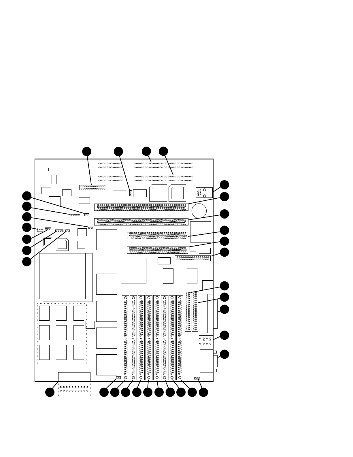
Table 1 lists the features of the AlphaPC 164 motherboard. Figure 1 shows
the board outlines, and identifies the location of jumpers, connectors, and
major components. Table 2 lists and defines these items. Refer to Section 4 for
connector pinouts. Refer to Section 3 for jumper configurations.
Table 1 AlphaPC 164 Features
Feature Description
Microprocessor Digital Semiconductor 21164 Alpha microprocessor (64-bit
RISC)
Chipset Digital Semiconductor 21172 core logic chipset, consisting
of one control chip and four data chips, that provides an
interface to system memory and the PCI bus
DRAM memory 16-MB to 512-MB memory array—One bank of either 4
(128-bit) or 8 (256-bit) commodity, 36-bit, 70-ns SIMMs
Caching
L1 Icache
L1 Dcache
L2 Scache
L3 backup cache
8-KB, direct-mapped, instruction cache on the CPU chip
8-KB, direct-mapped, data cache on the CPU chip
96-KB, three-way, set-associative, write-back, unified
instruction and data cache on the CPU chip
Onboard 1-MB, direct-mapped, synchronous SRAM backup
cache with 128-bit data path
I/O and miscellaneous
support 32-bit and 64-bit, 33-MHz PCI
Four dedicated PCI expansion slots (two 64-bit)
PCI/IDE control (CMD646)
Intel 82378ZB PCI-to-ISA bridge chip
Two dedicated ISA expansion slots
SMC FDC37C935 combination chip provides control for
diskettes, two UARTs with modem control, parallel port,
keyboard, mouse, and time-of-year clock
1-MB flash ROM
Firmware Windows NT ARC firmware
3

Figure 1 AlphaPC 164 Jumper/Connector/Component Location
MK−2306−35
Cache SRAM (L3)
U15
U34 U35
U41
U25
U22
U48
U29
U21
U49 U50
U40
U51
U52
U39
U36
J30 J31 J35 J33
J28
B1
J3
1
2
1
3
3113 14
1512
25
26
20 11
10 1
View from edge
U2
U18
U14
U10
U5
U16 U17
U11 U12
U6 U7
J25
J27
J21
J22
J23
J24
J4
J32
J29
J26
J20
J19
J18
J13
J14
J16
J15
J1 J5 J6 J7 J8 J9 J10 J11 J12 J2
12
11
1
22
33
34
39 40 39 40
3
Top: Mouse
Bottom: Keyboard
Top: COM1
Bottom: COM2
4

Table 2 AlphaPC 164 Jumper/Connector/Component List
Item Number Description Item Number Description
B1 RTC battery (CR2032) J1 Memory bus width jumper
J2 Fan power, enclosure (+12V) J3 Power (+3V, +5V, -5V, +12V, -12V)
J4 COM1/COM2 (DB9) connectors J5 DRAM SIMM 0 [35:0] connector
J6 DRAM SIMM 1 [71:36] connector J7 DRAM SIMM 2 [107:72] connector
J8 DRAM SIMM 3 [143:108] connector J9 DRAM SIMM 4 [179:144] connector
J10 DRAM SIMM 5 [215:180] connector J11 DRAM SIMM 6 [251:216] connector
J12 DRAM SIMM 7 [287:252] connector J13 IDE drive 2/3 connector
J14 IDE drive 0/1 connector J15 Keyboard/mouse connectors
J16 Parallel I/O connector J18 Diskette (floppy) drive connector
J19 PCI slot 3 (32-bit) J20 PCI slot 2 (32-bit)
J21 Microprocessor fan/fan sense
connector J22 Enclosure fan +12V power connector
J23 Speaker connector J24 Reset button connector
J25 Halt button connector J26 PCI slot 1 (64-bit)
J27 Power LED connector J28 Hard-drive LED connector
J29 PCI slot 0 (64-bit) J30 Configuration jumpers
J31 Flash update enable/disable jumper J32 SROM test port connector
J33 ISA slot 1 J35 ISA slot 0
U2 Data switch 0 (DSC 21172-BA) U5 to U7 Cache SRAM (L3)
U10 to U12 Cache SRAM (L3) U14 Data switch 1 (DSC 21172-BA)
U15 to U17 Cache SRAM (L3) U18 Data switch 2 (DSC 21172-BA)
U21 Microprocessor, socketed
(DSC 21164 Alpha) U22 Data switch 3 (DSC 21172-BA)
U25 I/O interface and address control
(DSC 21172-CA) U29 IDE controller
U34 Microprocessor clock crystal, 36.66-
MHz (default), socketed U35 Microprocessor clock PLL (TriQuint
TQ2061)
U36 System clock PLL (CDC 2586) U39 Serial ROM, socketed
(Xilinx XC17128D)
U40 PCI-to-ISA bridge (Intel 82378ZB) U41 Combination controller, Super I/O
(SMC FDC37C935)
U48 Flash ROM (1MB) U49 PCI arbiter PAL
U50 PCI interrupt request PAL U51 Power controller
U52 Power sense — —
5

2.1 Power Requirements
The AlphaPC 164 motherboard has a total power dissipation of 116 W,
excluding any plug-in PCI and ISA devices. Table 3 lists the power
requirement for each dc supply voltage.
The power supply must supply a DCOK signal to the system reset logic.
Table 3 Power Supply dc Current Requirements
Voltage/Tolerance Current1
+3.4 Vdc, ±3% 5.0 A
+5 Vdc, ±5% 12.0 A
–5 Vdc, ±5% 0 A
+12 Vdc, ±5% 1.0 A
–12 Vdc, ±5% 100.0 mA
1Values indicated are for an AlphaPC 164 motherboard (64MB DRAM) excluding adapter cards
and disk drives.
Caution: Fan Sensor Required
The 21164 microprocessor cooling fan must have a built-in sensor that
will drive a signal if the airflow stops. The sensor is connected to
motherboard connector J21. When the signal is generated, it resets the
system.
6

2.2 Environmental Requirements
The 21164 microprocessor is cooled by a small fan blowing directly into the
chip’s heat sink. The AlphaPC 164 motherboard is designed to run efficiently
by using only this fan. Additional fans may be necessary depending upon
cabinetry and the requirements of plug-in cards.
The AlphaPC 164 motherboard is specified to run within the environment
listed in Table 4.
Table 4 AlphaPC 164 Motherboard Environmental Requirements
Parameter Specification
Operating temperature 10°C to 40°C (50°F to 104°F)
Storage temperature –55°C to 125°C (–67°F to 257°F)
Relative humidity 10% to 90% with maximum wet bulb temperature 28°C
(82°F) and minimum dew point 2°C (36°F)
Rate of (dry bulb)
temperature change 11°C/hour
6
2°C/hour (20°F/hour
6
4°F/hour)
2.3 Physical Parameters
The AlphaPC 164 motherboard is an ATX-size printed-wiring board (PWB)
with the following dimensions:
• Length: 30.48 cm (12.0 in. ±0.0005 in.)
• Width: 24.38 cm (9.6 in. ±0.0005 in.)
• Height: 6.0 cm (2.4 in.)
The motherboard can be used in certain desktop and deskside systems that
have adequate clearance for the 21164 microprocessor heat sink and fan.
All ISA and PCI expansion slots are usable in standard desktop or deskside
enclosures.
7

3 AlphaPC 164 Jumper Configuration
The AlphaPC 164 motherboard has three groups of jumpers at location J1,
J30, and J31. These jumpers set the hardware configuration and boot options.
Figure 1 shows the jumper location on the AlphaPC 164 motherboard. Figure 2
shows the jumper functions for each group. Section 3.1 through Section 3.7
describe the jumper configurations.
3.1 Memory Bus Width Jumper (J1)
The memory bus width can be either 128-bits (J5 through J8 populated with
SIMMs and J9 through J12 empty) or 256-bits (J5 through J12 populated with
SIMMs). When using a memory bus width of 128-bits, jumper J1 must be in.
When using a memory bus width of 256-bits, jumper J1 must be out.
3.2 System Clock Divisor Jumpers (IRQ3 through IRQ0)
The system clock divisor jumpers are located at J30—1/2 (IRQ3), J30—3/4
(IRQ2), J30—5/6 (IRQ1), and J30—7/8 (IRQ0). The jumper configuration
set in IRQ3 through IRQ0 determines the frequency of the microprocessor’s
system clock output. These four jumpers set the speed at power-up as listed
in Figure 2. The microprocessor frequency divided by the ratio determines the
system clock frequency.
3.3 Bcache Size Jumpers (CF1 and CF2)
The Bcache size jumpers are located at J30—11/12, CF1 and J30—13/14, CF2.
These jumpers configure the Bcache as specified in Figure 2.
3.4 Bcache Speed Jumpers (CF4 and CF5)
The Bcache speed jumpers are located at J30—17/18, CF4 and J30—19/20,
CF5. These jumpers select the Bcache timing parameters used to compute a
value that is loaded into the microprocessor’s Bcache configuration register at
power-up time. Because the Bcache SRAMs are soldered onto the board, the
default jumper configuration selecting an SRAM access time of 9 ns as shown
in Figure 2 will always be used.
8

Figure 2 AlphaPC 164 Configuration Jumpers
J30 System Configuration Jumpers
IRQ3 1
3
5
7
9
11
13
15
17
19
21
23
25
CF0
CF4
CF5
CF6
CF7
CF1
CF2
CF3
Mini−Debugger (Default Out)
Boot_Option (Default Out)
Reserved (Default Out)
IRQ0
IRQ1
IRQ2
Reserved (Default Out)
Not Used
Frequency
333 MHz
Ratio IRQ3 IRQ2 IRQ1 IRQ0 Comments
All other combinations
10 Out In Out In
In Out Out
Out In In
Out In Out
366 MHz
400 MHz
433 MHz
11
12
13
Out
Out
Out Reserved
Bcache Size Out
Out
All other combinations
CF1 CF2 Comments
1MB Out
In2MB Reserved
Default
Bcache Speed Out
All other combinations
CF4 CF5 Comments
9 ns Out Reserved
Default
MK−2306−36
1
2
32 to 3 In = Enable (Default)
1 to 2 In = Disable
1
2
In = 128−Bit Bus
Out = 256−Bit Bus
Note: Jumper must be out when all
eight DRAM SIMM sockets are populated.
J31 Flash ROM Update Jumper
J1 Memory Bus Width Jumper
300 MHz 9 Out In OutIn
9

3.5 Mini-Debugger Jumper (CF6)
The Mini-Debugger jumper is located at J30—21/22 (CF6). The default position
for this jumper is out (Figure 2). The Alpha SROM Mini-Debugger is stored
in the SROM. When this jumper is in it causes the SROM initialization to
trap to the Mini-Debugger (communication through connector J32) after all
initialization is complete, but before starting the execution of the system flash
ROM code.
3.6 Boot Option Jumper (CF7)
The boot option jumper is located at J30—23/24 (CF7). The default position for
this jumper is out (Figure 2). This jumper selects the image to be loaded into
memory from the system flash ROM. With the jumper out, the Windows NT
ARC firmware is loaded. With the jumper in, the fail-safe booter is loaded. For
more information about the fail-safe booter, refer to Section 8.3.
3.7 Flash ROM Update Jumper (J31)
When J31—2/3 are jumpered together (default), the flash ROM is write-
enabled. When J31—1/2 are jumpered together, the flash ROM is write-
protected.
10

4 AlphaPC 164 Connector Pinouts
This section lists the pinouts of all connectors (see Tables 5 through 21). See
Figure 1 for connector locations.
Table 5 Peripheral Component Interface (PCI) Bus Connector Pinouts
Pin Signal Pin Signal Pin Signal Pin Signal
32-Bit and 64-Bit PCI Connectors (J19, J20, J26, J29)
A1 TRST# A2 +12V A3 TMS A4 TDI
A5 VDD A6 INTA A7 INTC A8 VDD
A9 — A10 VDD A11 — A12 GND
A13 GND A14 — A15 RST# A16 VDD
A17 GNT# A18 GND A19 — A20 AD[30]
A21 +3V A22 AD[28] A23 AD[26] A24 GND
A25 AD[24] A26 IDSEL A27 +3V A28 AD[22]
A29 AD[20] A30 GND A31 AD[18] A32 AD[16]
A33 +3V A34 FRAME# A35 GND A36 TRDY#
A37 STOP# A38 STOP# A39 +3V A40 SDONE
A41 SBO# A42 GND A43 PAR A44 AD[15]
A45 +3V A46 AD[13] A47 AD[11] A48 GND
A49 AD[09] A50 Not used A51 Not used A52 C/BE#[0]
A53 +3V A54 AD[06] A55 AD[04] A56 GND
A57 AD[02] A58 AD[00] A59 VDD A60 REQ64#
A61 VDD A62 VDD B1 -12V B2 TCK
B3 GND B4 TDO B5 VDD B6 VDD
B7 INTB B8 INTD B9 PRSNT1# B10 —
B11 PRSNT2# B12 GND B13 GND B14 —
B15 GND B16 CLK B17 GND B18 REQ#
B19 VDD B20 AD[31] B21 AD[29] B22 GND
B23 AD[27] B24 AD[25] B25 +3V B26 C/BE#[3]
B27 AD[23] B28 GND B29 AD[21] B30 AD[19]
B31 +3V B32 AD[17] B33 C/BE#[2] B34 GND
B35 IRDY# B36 +3V B37 DEVSEL# B38 GND
B39 LOCK# B40 PERR# B41 +3V B42 SERR#
B43 +3V B44 C/BE#[1] B45 AD[14] B46 GND
B47 AD[12] B48 AD[10] B49 GND B50 Not used
B51 Not used B52 AD[08] B53 AD[07] B54 +3V
B55 AD[05] B56 AD[03] B57 GND B58 AD[01]
B59 VDD B60 ACK64# B61 VDD B62 VDD
(continued on next page)
11

Table 5 (Cont.) Peripheral Component Interface (PCI) Bus Connector Pinouts
Pin Signal Pin Signal Pin Signal Pin Signal
64-Bit PCI Connectors Only (J26, J29)
A63 GND A64 C/BE#[7] A65 C/BE#[5] A66 VDD
A67 PAR64 A68 D[62] A69 GND A70 D[60]
A71 D[58] A72 GND A73 D[56] A74 D[54]
A75 VDD A76 D[52] A77 D[50] A78 GND
A79 D[48] A80 D[46] A81 GND A82 D[44]
A83 D[42] A84 VDD A85 D[40] A86 D[38]
A87 GND A88 D[36] A89 D[34] A90 GND
A91 D[32] A92 — A93 GND A94 —
B63 — B64 GND B65 C/BE#[6] B66 C/BE#[4]
B67 GND B68 D[63] B69 D[61] B70 VDD
B71 D[59] B72 D[57] B73 GND B74 D[55]
B75 D[53] B76 GND B77 D[51] B78 D[49]
B79 VDD B80 D[47] B81 D[45] B82 GND
B83 D[43] B84 D[41] B85 GND B86 D[39]
B87 D[37] B88 VDD B89 D[35] B90 D[33]
B91 GND B92 — B93 — B94 GND
12

Table 6 ISA Expansion Bus Connector Pinouts (J33, J35)
Pin Signal Pin Signal Pin Signal Pin Signal
1GND 2IOCHCK# 3RSTDRV 4SD7
5VDD 6SD6 7IRQ9 8SD5
9–5V 10 SD4 11 DRQ2 12 SD3
13 –12V 14 SD2 15 ZEROWS# 16 SD1
17 +12V 18 SD0 19 GND 20 IOCHRDY
21 SMEMW# 22 AEN 23 SMEMR# 24 SA19
25 IOW# 26 SA18 27 IOR# 28 SA17
29 DACK3# 30 SA16 31 DRQ3 32 SA15
33 DACK1# 34 SA14 35 DRQ1 36 SA13
37 REFRESH# 38 SA12 39 SYSCLK 40 SA11
41 IRQ7 42 SA10 43 IRQ6 44 SA9
45 IRQ5 46 SA8 47 IRQ4 48 SA7
49 IRQ3 50 SA6 51 DACK2# 52 SA5
53 TC 54 SA4 55 BALE 56 SA3
57 VDD 58 SA2 59 OSC 60 SA1
61 GND 62 SA0 63 MEMCS16# 64 SBHE#
65 IOCS16# 66 LA23 67 IRQ10 68 LA22
69 IRQ11 70 LA21 71 IRQ12 72 LA20
73 IRQ15 74 LA19 75 IRQ14 76 LA18
77 DACK0# 78 LA17 79 DRQ0 80 MEMR#
81 DACK5# 82 MEMW# 83 DRQ5 84 SD8
85 DACK6# 86 SD9 87 DRQ6 88 SD10
89 DACK7# 90 SD11 91 DRQ7 92 SD12
93 VDD 94 SD13 95 MASTER# 96 SD14
97 GND 98 SD15 —— ——
13

Table 7 DRAM SIMM Connector Pinouts (J5 through J12)
Pin Signal Pin Signal Pin Signal Pin Signal
1GND 2DQ1 3DQ2 4DQ3
5DQ4 6DQ5 7DQ6 8DQ7
9DQ8 10 VDD 11 GND 12 A0
13 A1 14 A2 15 A3 16 A4
17 A5 18 A6 19 A10 20 DQ9
21 DQ10 22 DQ11 23 DQ12 24 DQ13
25 DQ14 26 DQ15 27 DQ16 28 A7
29 A11 30 VDD 31 A8 32 A9
33 RAS3 34 RAS2 35 DQ17 36 DQ18
37 DQ19 38 DQ20 39 GND 40 CAS0
41 CAS2 42 CAS3 43 CAS1 44 RAS0
45 RAS1 46 VDD 47 WE 48 NC
49 DQ21 50 DQ22 51 DQ23 52 DQ24
53 DQ25 54 DQ26 55 DQ27 56 DQ28
57 DQ29 58 DQ30 59 VDD 60 DQ31
61 DQ32 62 DQ33 63 DQ34 64 DQ35
65 DQ36 66 VDD 67 NC 68 NC
69 NC 70 NC 71 GND 72 GND
Table 8 IDE Drive Bus Connector Pinouts (J13, J14)
Pin Signal Pin Signal Pin Signal Pin Signal
1
RESET
2GND 3IDE_D7 4IDE_D8
5IDE_D6 6IDE_D9 7IDE_D5 8IDE_D10
9IDE_D4 10 IDE_D11 11 IDE_D3 12 IDE_D12
13 IDE_D2 14 IDE_D13 15 IDE_D1 16 IDE_D14
17 IDE_D0 18 IDE_D15 19 GND 20 NC (key pin)
21 MARQ 22 GND 23
IOW
24 GND
25
IOR
26 GND 27 CHRDY 28 BALE
29 MACK 30 GND 31 IRQ 32
IOCS16
33 ADDR1 34 NC 35 ADDR0 36 ADDR2
37
CS0
38
CS1
39
ACT
40 GND
14
Table of contents
Other AlphaPC Motherboard manuals