Altec 9860A User manual

..------ NOTICE ------,
Read this manual before operating
the ALTEC 9860A Active Equalizer.
ALTEC.
ALTEC.
FEATURES
9860A
ACTIVEEQUALIZER
OPERATING
INSTRUCTIONS
• 26 Band-Rejection Filters - l/3 Octave, ISO Center
Frequencies (40 Hz to 12 .5 kHz)
• High-Pass and Low-Pass Filters with Controls
• Front Panel Gain Control
• Transformer-Coupled Inputs and Outputs
• Hinged Front Cover Prevents Tampering with Controls
• Bypass Switch
• AC or Battery Operation
• Modular PCB Construction
• Underwriters' Laboratories Listed
Specifi.cations and romponents s11l,jc,·t to channc wit ho11t
notice. Overall 11erf or11rn nee will lie 1naintninr'd or im.proved.
1515 S. Manchester Ave., Anaheim, Calif. 92803
SOUND PRODUCTS DIVISION

DATA CONTENTS
Item Page Graphics Title Page
SPECIFICATIONS 3 Figure l Typical Resp_onse Curves for Various
Filter Settings 5
DESCRIPTION 4 Figure 2 Electrical Connections 6
MODIFYING THE9860A ACTIVE EQUALIZER
FOR LOW-LEVELSIGNAL APPLICATIONS 4 Figure 3 Bottom View 9860A ,
Cover Removed 6
MODIFYING THE 9860A ACTIVE EQUALIZER
FOR USEWITH8080A PINK NOISE GENERATOR 4 Figure 4 Converting to 240V ac,
50/ 60 Hz Power 7
INSTALLATION 6 Figure 5 Input and Output Conne ctions 7
MECHANICAL 6 Figure 6 Front View 9860A, Hinged Pane l
VENTILATION 6 Cover Open 8
ELECTRICAL 6 Table I Control and Indicator Functions 8
120V ac, 50/ 60 Hz Power Connection s 6
240V ac, 50/60 Hz Power Connection s 6
Battery Connection s 7
Figure 7 Typical Sound System Response
Curve Before EquaIizati on 9
Input Conne ctions 7
Output Connection s 7 Figure 8 Typical Sound System Response
Curve After Equalizatio n 9
OPERATION 8 Figure 9 Control Settings Record 9
CONTROLS AND IN DICATORS 8 Figure 10 Top View 9860A, Cover Removed 11
Use of Equalizer Controls 8 Figure 11 Schematic (2D700-6),
SERVICE 10 9860A Active Equalizer 14
ACCESS 10
Cover Remova l l0
Control Pane l Assembly Removal 10
Figure 12 Schematic (2C693-l), Low/Mid
Frequency Potentiometer PCB
Assembly 15
PARTSREPLACEMENT l 0 Figure 13 Schematic (2C694- l), High
Frequency Potentiometer PCB
Fuse Replacement l0 Assembly 15
Input and O utput Transformer Replacement 10
Pilot Indicator Replacement 10
Power Transistor Replacement 10
Figure 14 Schematic (2D697-2), Low
Frequency FiIter PCBAssembly 16
Printed Circ uit Board (PCB) Replacem ent l0 Figure 15 Schematic (2D698-2), Mid
l . Control PCB Replacement 11 Frequency Filter PCBAssembly 17
2 . Filter PCBReplacement 11
3. Potent iometer PCBReplacement 11 Figure 16 Schematic (2D699- 3), High
Frequency Filter PCBAssembly 18
APPENDIX A 13 Figure 17 Schematic (2D701-5), Control
PROCEDURETO MODIFY 9860A FOR LOW- PCBAssembly 19
LEVELSIGNAL APPLICATIONS 13
APPENDIX B 13
PROCEDURETO MODIFY 9860A FOR USE
WITH8080A PINK NO ISE GENERATOR 13
PARTSLIST 20
MAIN CHASSIS 20
- 2 -

SPECIFICATIONS
Type: Act ive 1/3-octove equalizer with 26
band-rejection filters
Operating Gain: -3 dB
Available Gain: 20 dB (to restore equa lization loss)
Input Level : +18 dBm maximum
Power Output: +15 dBm
Frequenc y Response: ±l dB from 20 Hz to 20 kHz
Distortion:
Input Impedance:
Load Impedance :
Noise Leve I:
Controls:
Less than 0.5 % total harmonic distor-
tion (THD)at rated output and restored
gain
15<.x-2or 6000, balanced input
15<.x-2or 6000, balanced output
82 dB below roted output
26 detented linea r slide filter controls
on 1/3 -oc tove ISO centers 40 Hz
through 12 .5 kHz. 15 dB depth each
center frequenc y, combining with ad-
jac ent filters at - 7 dB.
- 3 -
Control s (co ntinued): l detented linear slide reinsertion
GAIN control
Pilot Indicator:
2 four-posi tion interlocked pushbutton
switches:
HIGH PASS; OFF/ 40 Hz/ 80 Hz/
160 Hz; 18 dB/ octave rolloff
LOW PASS; OFF/ 6 kHz/ 12.5 kHz/
16 kHz; 18 dB/ octave rolloff
l push/ push BYPASS switch
Light -emitting diode
Power Requirements: l20 / 240V oc, 50/ 60 Hz , 35W
Operating
Temperature Range:
Dimensions:
Weight:
Color :
-or-
24/ 28V de at 1A
Up to 50°C (122°F)
5-l/4"H x 19"W x 8"D
17 poun ds
ALTEC Green on panel cover, black
matte finis h on inner panel

DESCRIPTION
TheALTEC9860A Active Equa lizer is anAcousta- Voicing® *
filter set equipped with 26 active, band-rejecti on filt ers and
additional high/ low pass fil ter selection to accu rate ly equal-
ize the entire audio spectr um of one sound system channel.
The 9860A enables adjustm e nt of the sound system so that the
loudspeaker and encl osed- room environment provide a flat
acoustical response for the listener's ear. Interna l gain cor-
rection restores the equali zed output to the original input
level.
Typical response curves for various filter settin gs are shown
in Figure 1.
MODIFYING THE 9860A ACTIVE EQUALIZER FOR
LOW-LEVEL SIGNAL APPLICATIONS
The9860AActiveEqua lizer is designed to operat ew ithanom-
inal input leve l of about +4 dBm. In many studio monitoring
situations, however, leve ls as low as -12 or -1 4 dBmare en-
countered at the monitor bus outputs, and drivin g the 9860A
at those levels degrad es the signal-to-noise capa bi lities of the
device.
*The exclusive Altec Acoust a-Voicing ® proc ess is patented
under Pat. No. 3,62 4, 298.
- 4 -
The 9860A is equipped with 15356A input and output transfor-
mers. These are 600/ 600-ohm device s and are used for isola-
tion only. If the 15095A transformers are used instead, the
600/15,000-ohm impedance transformation provides a 13 dB
voltage advan tage going into the equali zer circuitry, and
consequently that much more signal-to-noi se ratio.
Refer to Appendix A for the necessary modification procedure.
,---------NOTE---------,
After modification, clipping of input signal will
result for input levels exceeding approximately
+5 dBm.
MODIFYING THE 9860A ACTIVE EQUALIZERFOR USE
WITH8080A PINK NOISE GENERATOR
Substitution of the 8080A Pink Noise Gener ator for the norma I
input transformer of the 9860A provides great flexibility in
tailoring a noise source to thedesiredspect ruminawiderange
of environmen ts.
Refer to Appendix Bfor the necessary modification procedure.

9860A
~
..... ,v'V V AX~JI • ///
'"' (Y) X ) x~X ¥x1, I/ {/
.I \/\/ i/V u
~
V11 .I
~
I\(
•
2 3 4 567891 3 4567891 1000
FREQUENCY IN HERTZ
3 4 567891 2
20 100 10000 20000
a,
0
-;
a,
0
-;
a,
0
-;
26 l/3 Octave-Centered Filters at Max imum
Attenuation (-14 dB). Each Section
Plotted Independently
~
r7"
1
2 3 4567891 34567891 1000
FREQUENCY IN HERTZ
3 4567891 2
20 100 10000 20000
)
I
I
I
I
Single Filter, 1 kHz, Shown in Each Detented
Position of Attenuation
)"'
~
/ r-,, "-
~
/ '\
,,
J V i\ \
J \
I II \
J \
I 1
2 345 67891 3 45 67 89 1
1000
FREQUEN CY IN HERTZ
345 67891 2
20 100 10000 20000
i.-..
High-Pass and Low-Pass Functions (18 dB/ oct}
Plotted Indep endently
\ /
I
... l/
I\ -
~
r
y - y
2 3 4567891 3 456789 1
1000
FREQUENCY IN HERTZ
3 45 6 789 1 2
20 100 10000 20000
All Filter Sections Set at -7 dB Attenuation
lllusrrating Slight Degree of "Ripple"
(±l/2 dB} Characteristic of Proper
Interaction Between Sections
a,
0
-;
a,
0
-;
a,
0
-;
-I\
V -
~ J\JV
2 3 4567891
20 100
" r
i/\ VI vvv
34567891 1000
FREQUENCY IN HERTZ
I
I
I
r (\I
JV
V'/I/ l
34567891 2
10000 20000
Al I Fi Iter Sections Set for Fu 11Attenuation
-
2 3 4567891
20 100
I
I
1/\I
3456789 1
1000
FREQUE NCY IN HERTZ
/V"
3 4 567891 2
10000 20000
Two Adjacent Filters, 1 kHz and 1250 Hz,
Set for Ful I Attenuation
i--~
2 3 4567891
20 100
r-,,r\ I
I
J
3456789 1
1000
FREQUEN CY IN HERTZ
/---
34567 89 1 2
10000 20000
kHz Filter Set at -14 dB, 800 and 1250 Hz
Filters Set at -8 dB
Figure 1. Typica l Response Curves for Various Filter Settings
- 5 -

INSTALLATION
MECHANICAL
The 9860A may be mounted in a standard 19-in ch equipment
rack. Vertical rack space required is 5-1/4 inches. Use the
following procedure:
Step l. Remove four screw s securing front cove r; open and
lower cover .
Step 2. Install 9860A in equipment rack with a ppropriat e
four screws supplie d with unit.
Step 3. Close front cover and secure with four scre ws previ-
ously remove d .
VEN TILATION
The 9860A generates minim a l heat during normal use . Al-
though the amount of heat is re lati ve ly low, the unit must be
vent ilated to prevent exces sive tempera ture rise. Becau se
transistors are heat sensitive, the 9860A should no t be placed
adiacent to heat-generating equipment or in ar eas where am-
bient temperature exceeds 50°C (122°F).
If the 9860A is mounted in a n equipment rack or cab inet with
other heat-producing equipm e nt mounted abo ve and / or be low
(two or more 9860A 's or one 9860A with real t ime ana lyzer,
oscilloscope, etc.), space must be provided betwe en the units
or the 9860A may become too warm. A 1-3/ 4" perforated
panel is recommended for thi s purpose.
J.CUNE
i IATTERY
:u.v.o
-
lfl' LACt WITHTHE SA.METYPEfUSE
EXTIATT
GND
♦
2
4V
When severa I 9860A 's or other heat- producing units are
mounted in a sing le rac k or cab inet, acc eptab le air tempera-
ture may be in doubt. To determine tem perature cond iti ans,
operate the system until temperatures stab ilize, then measure
air temperature with a bulb-type ther mometer held at the
bottom of the uppermost 9860A. Do not let the thermometer
bu lb touch metal because the metal wil l probably be hotter
than the amb ient air. If air temperature could exceed 50°C,
the equipment shou ld be spaced furthe r apart or a blower
shou ld be insta lled to venti lat e the cabin e t.
ELECTRICAL
120V ac, 50/ 60 Hz Power Connections
Equipment supp lied for domestic use is provided with the
power transfo rmer strapped for 120 vo lts (terminals 2 to 3 and
4 to 5 on TB4). The power input name plate on the chassis
adiacent to the power cord is mounted to show the appropri-
ate side specifying the connections (see Figure 2). Verify
that lin e vo ltage is in accordance with the vo ltag e rating
before connecting the 9860A to line powe r .
240V ac, 50/ 60 Hz Power Connections
Export eq uip ment, specified, is provid ed with the power
transformer strapped for 240 vo lts (termi na ls 3 to 4 on TB4).
The power input namep lat e on the chas sis adiacent to the
power cord is mounted to show the appropr ia te side specifying
the connect ions. Use the following pro c edure to change a
unit strapped for 120V operation to 240V operation:
C\ASS IIwtMNGMAYIll USED
Figure 2. Electrical Connections
POWER TRANSISTOR(Q l) POWERTERMINALBOARD(TB4)
Figur e 3 . Bottom V iew 9860A, Cover Removed
- 6 -

240V ac, 50/ 60 Hz Power Connections (continu ed}
Step l . Remove seven screws securing bottom cover; Iift off
cover.
Step 2. Locate terminal board TB4 beneath power trans-
former T3.
Step 3. Remove strap "A" connecting terminals 2 and 3, and
remove strap "B" connec ting terminals 4 and 5; then
solder strap "C" to terminals 3 and 4 (see Figures 3
and 4).
Step 4. Remove voltage rating nameplate from chassis, re-
verse and reinstall to show 240V rating.
Step 5. Replace bottom cover and secure with seven scre ws
previously removed.
Step 6. Change ac line fuse (Fl) from the existing lA fuse
to a l/2A fuse (see Figure 2). Place a l/2A ac line
rating tag on tag on the back of the 9860A, abo ve
the AC LINE fuse.
BRN/WHT
REMOVESTRAPS"A" AND "B"
INSTALLSTRAP"C"
BLK
GRN
WHT
El
Wl
Figure 4. Converting to 240V ac, 50/ 60 Hz Power
Battery Connections
If desi red, the 9860A may be connected to an external
24/ 28V battery with minus (-) as ground. Terminals for the
de power connections are on TB3(see Figures 2 and l l ). If ac
power foils, transfer to de power is instantaneous, automatic
and silent.
-7-
Input Connections
Input to the 9860A is connected to the INPUT terminal board
(TBl} on the rear pane I of the chassis (see Figures 2, 5 and
l l}. Connections to ALTEC power amp Iifiers must be made
with two-conductor, twisted and shielded cable, such as
Belden 8450 or 8451 cable.
------NOTE
For amp Iifier connections, refer to
operating instructions for associated
ALTEC amplifier.
For 600-ohm balanced input applications with 9860A, con-
nect amplifier to terminals land 4 of TBl and strap terminals
2 and 3 (see Figure 5). Terminals 4 (common} and 5 (ground}
may also be strapped to prevent interference from stray elec-
trostatic radiation.
For 150-ohm balanced input applications with the 9860A,
connect amplifier to terminals 1 and 4 of TB] and strap ter-
minals l to 2 and 3 to 4 (see Figure 5). Terminals 4 and 5
may also be strapped to pre vent interference from stra y elec-
trostatic radiation.
Output Connections
Output from the 9860A is connected to the OUTPUT terminal
board (TB2) on the rear panel of the chassis (see Figures 2, 5
and 11). Terminal connections and cable requirements are
the same as described for input connections.
2
TB2
OUTPUT
3 4 5
TBI
INPUT
3 4
CONNECTIONS FOR 600 OHMS BALANCED INPUT AND OUTPUT
2
TB2
OUTPUT
3 4 5 2
TBI
INPUT
3 4
CONNECT IONS FOR 150 O HMS BALANCED INPUTAND OUTPUT
Figure 5. Input and Output Connections
5
5

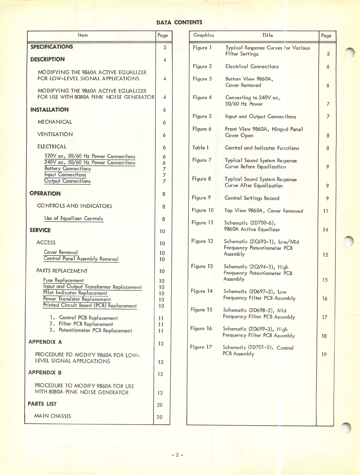
OPERATION Table I. Control ond Indica tor Functions
CO NTROLS AND INDICAT O RS
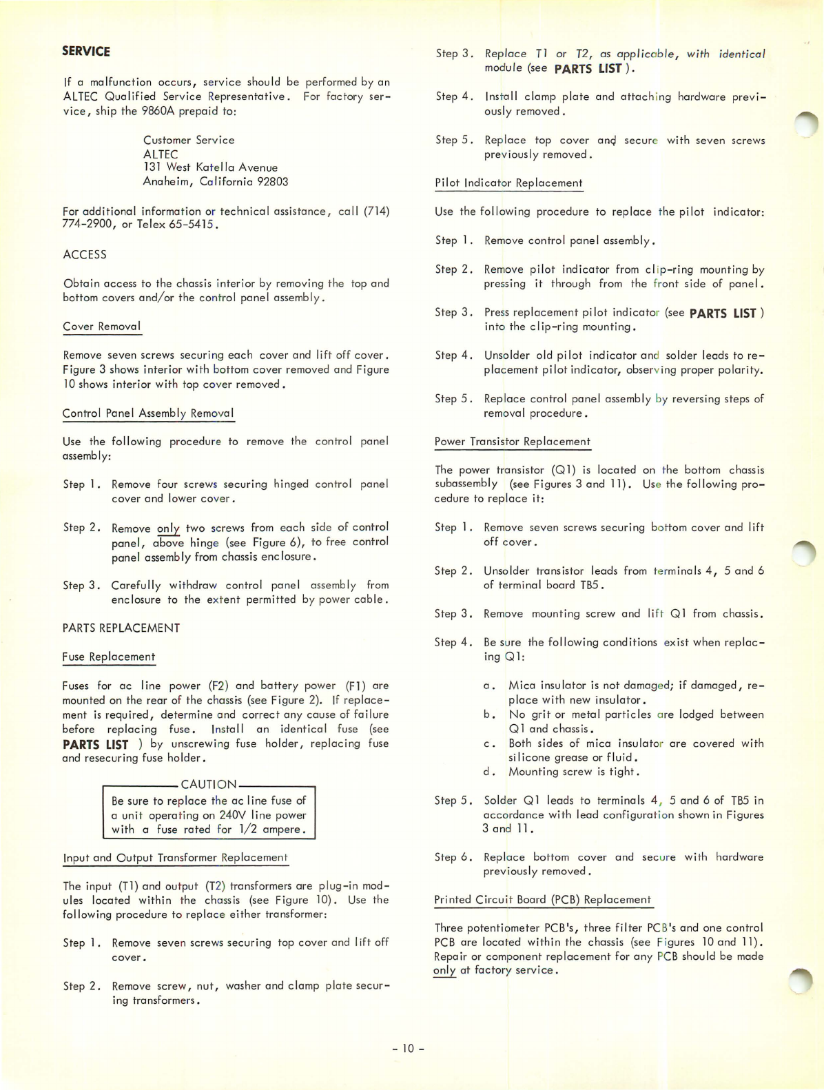
The pilot indica tor and al l operating controls ar e on the front
pan e l (see Figure 6). Thei r function s are descri bed in Table
I. A hinged cover preve nts inad vertent control changes.
When the hinged co ver is secured, onl y the BYPASS switch
and pilo t indicator are exposed.
Use of Equalizer Con trols
Although the filter controls are continuously variab le slide
potentiometers, they are det e nted in increment s of 1-1/2 dB.
ALTEC strong ly recommends that onl y the det ented pos itions
be used to guarantee prec ision resetting of the con trols.
Typica I sound system response curves before an d after equa 1-
izat ion are shown in Figures 7 and 8. A convenient method
of recording filter contro l se tt ings for future resetting of con-
tro ls for different installati ons or application s is show n in
Figur e 9.
On ly one pushbutto n at a ti me should be pressed on the HIGH
PASS se lector or LOW PASS selector. Two pushbuttons wiII
lock in for ei ther selector but an error in filt er frequency
inser tion wiII resu It.
The first attempt to smooth the house cur ve shou ld be limited
to one or two of the greate st peaks or va Ileys. After th is
initial smoothing, run a new house cur ve to check resu lts.
Continue adjusting one or two sections at a time, rep lot ting
the frequency response each time, un til the desired unifo rmit y
of response is achieved or unti I the correct ion capabi Iity of
the 9860A is exceeded.
After the best obtainab le house cur ve is achie ved with the
9860A fi lter controls, adjust the GA iN control to provide an
equa lized output leve l as high as the unequalized input
leve l. The GAIN control is detented in increm ents of 2 dB
and has a reinsertion range of +20 dB.
Nam e
Filter Controls
HIGH PASS Se lector
LOW PASS Se lector
GA IN Contro l
BYPASS Switch
Pilot Indicator
1/~ OCTAVf CENT ER FReQueNCV·H I
Function / Description
Twent y six detent e d, lin ear slide con-
tro ls, continuous ly variab le, gradu-
ated from O to - 15 dB. Each control
adjusts a 1/3-oct a ve band-rejection
filter. ISO cent er frequencies range
from 40 to 12,50 0 Hz. Fi Iter depth is
-15 dB on each center frequency,
combining with ad jacent filters at - 7
dB.
Four interlocked pushb utton switches
for OFF , 40 Hz, 80 Hz and 160 Hz.
Selects high pass filter to shape low-
frequenc y audio spectrum. Inserts -18
dB/ octa ve rolloff a t the selected cor-
ner frequency.
Four interlocked pushbutton switches
for OFF, 6 kHz, 12.5 kHz and 16
k Hz . Selects low pass filter to shape
high-frequency au d io spectrum. In-
serts -18 dB/ octa ve rolloff at the se-
lected corner freq uency.
De tented, lin ear sl ide contro l, con-
tinuous ly var iable over a 20 dB range.
Adju sts leve l of eq ua lized program to
match level of unequalized program.
Pushbutton switch for A/ B comparison
or bypassing 9860A . Options of mo-
mentar y action or pus h-and- lock.
Light-emitting dio de . Continuousl y
Iit when equa Iize r is in operation.
Periodicall y flashe s in bypass mode.
on ,,,
-- - -- - ----- - ------ - -- - - - - -~
-------- - -- - - - - - - - - ------_ ,
------------ - - -- - -- - - -----·
----------- - -- - -------- - --·
----- - ------ - - -----------_,,
----------- - - - - -----------··
Figure 6. Front View 9860A, Hinged Pane l Cover Open
- 8 -

I
--0
,
90
85
80
75
70
65
..J
fu60
al
"C 55
50
~
FREQUENCY IN HZ 90
85
80
75
70
65
&60
al
"C 55
50
----,
FREQUENCY IN HZ
--+-+- ..
t--l----
l-- f---1---•
·- ~J:::::::t=
1 2 3 4 5 6 7 8 9 10 11 12 13 14 15 16 17 18 19 20 21 22 23 24 25 26 1 2 3 4 5 6 7 8 9 10 ll 121314151617181920212223242526
4-0
'
I
d8
12
BAND NUMBER BAND NUMBER
Figure 7. Typical Sound System Response Curve Before Equalization Figure 8. Typical Sound System Response Curve After Equalization
50 63 80 100 125 160 200 250 315 400
CIRCLEDETENTSETTINGFOR EACHCONTROL ANO WRITE"IN" FOR EACHSELECTEDPUSHBUTTON
1/3 OCTAVECENTERFREQUENCY- HZ
500 630 800 1000 1250 1600 2000 2500 3150 4000 5000 6300 8000 10000 12500
Figure 9. Control Settings Record
GAIN
12
16
20
HIGH PASS
EJ
OFF
40 HZ
80 HZ
160 HZ
LOWPASS
EJ
6KHZ
12.5 KHZ
16 KHZ
OFF

SERVICE
If a maIfunction occurs, service shou Id be performed by an
ALTEC Qualified Service Represen tati ve. For factory ser-
vice, ship the 9860A prepaid to:
Custo mer Service
ALTEC
131 West Katella Avenue
Anaheim, Ca lifornia 92803
For additional informa tio n or techn ical assistance, ca ll (714)
774-2900, or Telex 65-5415.
ACCESS
Obtain access to the chassis interior by removing the top and
bottom covers and / or the co ntrol panel assembl y.
Cover Removal
Remove seven screws securi ng each cover and lift off cover.
Figure 3 shows interi or with bottom cover remo ved and Figure
lO shows interior wit h top cover removed .
Control Panel Assembl y Removal
Use the fol lowing procedure to remove the control panel
assembly:
Step 1. Remove four screw s securing hinged control pane l
cover and lower cover.
Step 2. Remove onl y two screws from each side of contro l
panel, above hing e (see Figur e 6), to free control
panel assem bly from chassis enclosure.
Step 3. Carefully withdraw control panel assembl y from
enclosure to the extent permitted by power cable.
PARTSREPLACEMENT
Fuse Replacement
Fuses for ac Iine power (F2) and battery power (F1) are
mounted on the rear of the chassis (see Figure 2). If replace -
ment is required, det ermine and correct any cause of failure
before replacing fuse. Install an identica l fuse (see
PARTSLIST ) by unscrewi ng fuse holder, rep lacing fuse
and resecuring fuse holder.
.------ CAUTION-----
Be sure to replace the ac Iine fuse of
a unit opera ting on 240V line power
with a fuse rated for 1/2 ampere.
Input and Output Transformer Replacement
The input (Tl) and output (T2) transformers are plug-in mod-
ules located within the chassis (see Figure 10) . Use the
following procedure to repla ce either transformer :
Step l. Remove seve n screws securing top cover and Iift off
cover.
Step 2. Remove screw, nut, washer and clamp plate secur-
ing transform ers.
- 10 -
Step 3. Replace Tl or T2, as opp/ icable, with identical
module (see PARTSLIST).
Step 4. Install clamp plate and attac hing hardware previ-
ously removed.
Step 5. Replace top cover an<;l secu re with seven screws
pre viously removed.
Pilot Indicat or Replacement
Use the following procedure to replac e the pilot indicator:
Step l. Remove contro l panel assembly.
Step 2. Remove pilot indicator from cl ip-ring mounting by
pressing it through from the front side of panel.
Step 3. Press replacement pi lot indicato r (see PARTSLIST)
into the clip-ring mounting.
Step 4. Unsolder old pi lot indicator an d solder lead s to re-
placement pilo t indicator, obse rv ing proper polarity.
Step 5. Replace control panel assembly by reversing steps of
removal procedure.
Power Transistor Replacement
The power transistor (Ql) is located on the bottom chassis
subassembly (see Figures 3 and ll). Use the following pro-
cedure to replace it:
Step l . Remove seven screws securing bottom cover and Iift
off cover.
Step 2. Unsold er transistor leads from terminals 4, 5 and 6
of term inal board TBS.
Step 3. Remove mounting screw and Iift Q l from chassis.
Step 4. Be sure the following conditions exist when replac-
ing Ql:
a. Mica insulator is not damag ed; if damaged, re-
place with new insulator.
b. No grit or metal particles are lodged between
Ql and chassis.
c. Both sides of mica insulato r are covered with
silicone grease or fluid.
d. Mounting screw is tight .
Step 5. Solder Ql leads to terminals 4 , 5 and 6 of TBSin
acco rdance with lead configurat ion shown in Figures
3 and l l.
Step 6. Replace bottom cover and secure with hardware
previously removed.
Printed Circuit Board (PCB) Replacement
Three potentiometer PCB's, three filter PCB's and one control
PCB are located within the chassis (see Figures lO and l l).
Repair or component replacement for any PCB should be made
~
at factory service .

(A6)
HIGH-FREQUENCY FILTERPCB (A4)
MID-FREQUENCY FILTERPCB
CONTROL
(Al,A3)
LOW/Ml D-FREQUENCY
POTENTIOMETER PCB
(A2)
LOW-FREQUENCY FILTERPCB
Figure 10. Top View 9860A, Cover Removed
....----- CAUTION------,
Filter PCB's have several factory-
adjusted potentiometers. Their ad-
justments must not be disturbed be-
cause any changes result in misalign-
ment of the corresponding band-re-
jection filters. Adjustment of these
potentiometers should be done only
at factory service. --
A new or repaired PCB may replace a failed PCB to restore
operation. Remove the control panel assembly, then use the
applicable replacement procedure for the failed PCB.
.------ CAUTION----~
When removing and replacing any
PCB, do not warp_, bend or twist the
board """'"orconductor may fracture.
1. Control PCB Replacement
Step a. Remove two screws at front end of PCB which
secure it to spacers on chassis.
Step b. Carefully lift rear of PCB to free connector
pins. Take care that control buttons do not
bind in control panel while removing board.
Step c. Insert control buttons of replacement PCB
through appropriate holes in control panel and
position connector pins of replacement PCB
over receptacle. Verify that all PCB connec-
tor pins mate properly with receptacle, then
press PCB firmly into receptacle. Be careful
not to warp, bend or twist the board.
Step d. Align PCB mounting holes with spacers on
chassis and secure PCB with two screws previ-
ously removed.
- 11 -
Step e. Replace control panel assembly by reversing
steps of remove I procedure.
2. Filter PCB Replacement
Step a. Remove four screws from rear of board which
secure it to spacers on potentiometer PCB.
Step b. Carefu Ily Iift PCB to free connector pins; if
necessary, remove plastic cable clamps from
cable harness.
Step c. Carefully remove all wire connections from
PCB, tagging each connector as removed with
wire color / relationship •
Step d. Attach wire connectors to replacement PCB in
accordance with tagging (see Step c).
Step e. Position connector pins of replacement PCB
over receptacle, then press PCB firmly into re-
ceptac Ie. Be carefu I not to warp, bend or
twist the board.
Step f. Align PCB mounting holes with spacers on po-
tentiometer PCB and secure it with four screws
previously removed.
Step g. Replace any cable clamps removed in Step b.
Step h. Replace control panel assembly by reversing
steps of remove I procedure.
3. Potentiometer PCB Replacement
Step a. Remove nine plastic slider tips from filter con-
trols of PCB being replaced; the tips are press-
fitted and may be pulled free.

Step b. Remove four screws securing PCB assembly to
front panel.
Step c. Remove four threaded spacers securing potenti -
ometer PCB to filter PCB.
Step d. Carefull y lift PCB to free connector pins.
Step e. Position conn ec tor pins of replacement PCB
over rec eptac le. Verify that all PCB connector
pins mote prop erly with receptacle, then press
PCB firmly int o receptacle. Be careful not to
warp, bend or twist the board.
- 12 -
Step f. Secure potentiometer PCB to fil ter PCB with
four thread ed space rs previously removed.
Step g. Align spacer mounting holes with holes in front
panel and secure PCB with four screws previ-
ously removed.
Step h. Press nine plastic slider tips, previously re-
moved, onto filter controls .
Step i. Replace control panel assembly by reversing
steps of removal procedure.

APPENDIX A
PROCEDURETO MODIFY 9860A FOR LOW-LEVEL
SIGNALAPPLICATIONS
Step 1• Removetop and bottom covers of 9860A.
Step 2. Rewiresockets of transformers Tl and T2 to accommo-
date 15095Atransformers inaccordance with the fol-
lowing wiring diagrams.
~
T2
~
P4 15095A
L!J
TB2
Step 3. Complete procedure for Control Panel Assembly Re-
moval given on page 10. Remove Control PCBas-
sembly(see Figure 10 and procedure for Control PCB
Replacement given on page 11).
Step 4. Locate R36on Control PCBassembly as shown below,
and replace R36with a 1SKQ resistor.
Step 5. Replace Control PCBassembly in 9860A (reverse pro-
cedure given on page 11). Replace Control Panel
Assembly in 9860A(reverse procedure given on page
10).
APPENDIX B
PROCEDURETO MODIFY 9860A FOR USEWITH
8080A PINK NOISE GENERATOR
Step 1• Removetop and bottom covers of 9860A.
Step 2. Install a 5100, 1/2-watt resistor from pin 7to pin 1
on TBS(see Figures 3 and 11).
- 13 -
CJ
CJ
CJ
+
C 7
0
CJ
CJ
CJ
0
+
C 6 :1
CJ J3
J4
:J
CHANGER36
FROM620D
TO 15KD
Step 6. Install 15095A transformers in sockets for Tl and T2
(see Figure 10 and procedure for Input and Output
Transformer Replacement given on page 10.
Step 7. lnstalI Control Panel Assembly top and bottom covers
on 9860A (reverse sequence of Step 1).
Step 3. Install a jumper wire from pin 1 of TBSto pin 5 on
transformer Tl socket.
Step 4. lnstal I a 1500 µF, 25V de capacitor between pin 1 of
TBSandground lug of capacitor Cl (negative side of
capacitor is ground).
Step 5. Replace transformer Tl with 8080A (see Figure 10
and procedure for Input and Output Transformer Re-
placement, page 10).
Step 6. Install top and bottom covers of 9860A.

.i,..
Al
J_2
POTENTIOMETER
BOARD
27- 01- 04 2469
JO J 4 J5 JE, J7 JB
1231231231231 23 1 23 1 23 1 23
P1 P2 P3 P4 PS P6 P7 PB
LOW FRE Q FILTER
A2 27- 01- 0424 20
PIO
m
Pl [ i 2 3 4 5 6 7
y y y y - y
234567 J 3
2. CAPACITANCE VALU ES IN MICROFARAOS - 20 .. 1QOD/o
I. RESIST A NCE VAL UES ARE IN OHMS ! 10~1.
NOTES, UNLESSOTHERWISE1NOICATEO.
A3
A4
POTE NTIOM ETER
BOARD
27-0l-042469
J4 J5 J6 J7
MID FREQ FILTER
27- 01-042440
P 10
t -i - r-1
t=ttti
pzr::r=-1 i 1 Y
~
; )
y - y y--y-yyy
234567
+ 24
EXT BATT
J2 A7
CONT RCL 8 0 ,\l<C
27- 0 1-04 24 70
J B J9
C2
~~so
A5
POTENTIOMETER
BOARD
27- 0 1- 042480
R___Lll_!_S...!,_O_!<S
O l ] 12.F.1.., ,:::o :z. pea ,.,
o.;J..IJ•wl\~.Ja,J"~,..,"l 'o. ~I
t- 'o~
@l oo
~foo
c1£12)/.i~Ia.
~,,,...-~-·_..~---=-~
RE-RDUTW CR-I -ADDED
F3 -ECO/135B
ADDED C R4 ~___!__!__g!_Q___J__g_F"
Dbr.LIJ LI TIIRLI~, ,C".3771/itlt'&.
li'£JO?a:JJPa-Ao/I>'arO / I' C.l..
l .:'.31 231231231 23 1 ?.3 1 2 3 1 23123
Pl P2 P3 pa P 5 P 6 P 7 PS P9
A6 HIGH FREQ FILTER
27-01-042450
PIO
wwn
P3!\ j
~ ~ ~
t !1
y y y y y y y
C4
J;.0,IDISC,
3 4 5 E, 7
J I + I
Pl -2 >a</CR3
;sl=./POWER INDICATOR
JUTFUT
110/120 VAC
:::::·:::.:: ·.:: ::":.:.. .. . ·; ::···: · 71 SK'.Hc ,v,ATIC-
l
""",.o'"'""'"•"'cuow ,,,.,_,_,
>--. -- - -- . ' " " 9 85 0A
1----+-l- - •·
00
_ ACTIVE EQUALIZ rn
;'~G,C1 A,
ALTEt
-- ·
/1 ~.t~lM>f,oJrtt.i,,,_
..,N,..,.,,..c:,.u"o""''"'
D1207C0-06
l ~ l
Figure 11. Schematic (2D700-6), 9860A Active Equalizer

JI J2 J3 J4 JS J6 J7 J8 J9
2 3 2 3 2 3 2 3 2 3 2 3 2 3 2 3 2 3
2 2 2 2 2 2 2 2
RI R2 R3 R4 RS R6 R7 R8 R9
Figure 12. Schematic (2C693-l ), Low/Mid Frequency Potentiometer PCB Assembly (Al, A3)
JI J2 J3 J4 JS J6 J7 J8 J9
2 3 2 3 2 3 2 3 2 3 2 3 2 3 2 3 2 3
-f- -- - - -- - - -
3
2 2 2 2 2 2 2 2 2
RI R2 R3 R4 RS R6 R7 R8 R9
Figure 13. Schematic (2C694-1), High Frequency Potentiometer PCBAssembly (AS)
- 15-

0-
Pi
VI
P2
3 O.LL TRANS ISTORS ARE: 010P4/2N5308
RS
75 0
V2
V.2 V l 2
2. ALL RESISTORS ARE IN OHMS, 1/4 WATT 5%
I. ALL CAPACITORS ARE IN M\CAOFAAADS
NOTES, UNLESSOTHERWISEINOICATEO.
P3
V I
RO,
P4
R31
7'0
P5 P7 p 9 IZ[;.I.. F<=>IZ. PJZ.o:>O
-z..IACC£.D CAf:U:-
V2 V.1 2
~
V.2 Vl 2
~
V1R89
IM
10~
VI 2
R9~
20K
V2
t l5/10!
6
R64
750
na
VI
2K '-------r,
R65
20K
PG
V2
PS
VI
""
750
R87
20K
R77
2)( R90
2.21<
,o-.
P.91 R9~
IOK 12.7K
10¾ Ill.
+
c..L C45
5/10
RSG
270
R97
750
V2
R78
IM
10,
CABLE
o• PIO /'
-I( 1
)~ i I INPUT
+ ~10
?.",• : :, 71.
~>---t2VI
--+»--~3 NOT USED
~>---t4 GN0
"41>-----t-5 V2
-fn---~6 NOT USED
l,.>-----9-7 OUTPU T
Pl
SC HEMAT IC-
LOW Fl"IE,J '.'ii..T~R
B'JARC,
Figure 14, Schematic (20697-2), Low Frequenc y Filter PCB Assembl y (A2J
ALTEC
- ·
•-_, ~l ..-.._
AMAHKIW . CAU...,.__..,
D120697 -t
I
~
I

'-J I
Pl P3
V2 VI V2 V I ?.
I VI
R9
750
V2
IRl2
IM
~lot----~
-iT 5/JO
R20
750
P2
3. ALL TRANSI STOR S ARE D16P4.'2 NS3C.8
10¾
2. A LL RESISTORS ARE IN OH MS , 1/4 WATT 5%
\, ALL CAPAC ITOR S ARE IN MICROFARAD$
NOTES: UNLESSOTHERWISEINOICATEO.
R4
R42
750
VI
R31
7'0
2• "------- -+--+
R4'
P4
P5 P7
V(: 1
1 ~2 I - -
~
V.2 VI 2
IM 31
IO'T. t,,±
110
~i31
~~
~5
V2 V '
~R'4
IM
R65
20K
PG
n6
V2
t56
IM
ltlY.
1'15/10
•
2K
RB6
750
V I
RB7
20K
PS
1-lSO
:?.; K
IOY.
V2
2
~9 1
IU K
10¾
tR78
,M
,o,
izet.. F="o<z.?rz.oo
p 9 z 1,A.ooE.D <::A'P.,U. i. P 2. JaJl,ftJ
l?<J
~
-;~
~~~
,1~1&
R)7
75 0
i_LCABLE
PIO
-- --+----,> I I tr~PUT
t-+z VI
"°1>--?3 NOT US[U
__ri >----r)-4 GND
7
➔
-+5
V2
-+ -+ 6 NOT USED
L----4 1>-----------4,.7OUTPl.11
.......~,--".............t-,· - ·1-1-.,
~~fA
P2
SCHEM.ATIC-
MID FREQ FILTER
BOil.RD ALTEC
-·
.--"' 0.V":Yt ... --
........... ,.. . c ............ ......
D12D698 -Z
I ~ 1
Figure 15 . Schemat ic (2D698 -2 ), Mid Frequenc y Filter PCB Assembl y (A4)

(X)
Pi P3
V2 VI 2 3 V2 VI 2
VI
2,2K.00525 Rl6 I
Rl9 10.0K
270 I}'.
c,o
-tf5/10 R20
750
R22
I.SK
R21
vv...
20K
P2
~Rl4
I0K
10·1.
R9
75 0
3. ALL TRANS I STORS ARE D16P4/2N530S
-tf5/10i R42
750
VI
R31
750
R4
I.SK~-----+--<
R43
20~
P4
2. ALL RES ISTORS ARE IN OH MS, 1/4 WATT 5%
\, ALL CAPAC ITOR S ARE IN MICROFA.RAOS
NOTES: UNLESSOTHERWISEINOICATEO.
P5
V2 VI 2 3 V2 VI
'
R45 ~~ '" I
IM I + 10¾
10Y. 20K 5110 RSS R68
1.5K '">?M
na
V2 V I
R65
20K
P6
2
r·
20K
V2
t R56
j',M
,or.
P7
I
PA
VI
R87
20K
; V2
i t"
R77 I 11
~'"1.
f,.SK
+C4l
5/10
VI 2 p 9
h~ C4,
ve
R91
12K
10,-o
.,.
C36
5/IO
R9c
270
R_~S
3.311'
27PF
QIS
AL4l440
R92
330
R93
2.7K
+0/50
-0:SLE
PIO r
~-----!-+-----+-- -- --'~ I INPUT
4b>-\3>2V I
~---- +--------'-' 1 >--------?3 SECTION 91N
~>--------?4 GN0
~
4f>----t5 V2
L_-- -----+1-----4J)) - -- ~.6SECTION 8 OUT
-- - --"~7 OUTPUT
....,.,- ,.., ..-....
'" "··~""' ··~" ... I ,_1-1 , I
P3
SCHEMATIC-
Ht FREQ FI LTER
BOARD
Figure 16. Schematic (20699-3), High Frequ ency Filter PCB Assembly (A6)
ALTEC
- ·
,. ,,,,,,_., /J,1"V1"9.u ... i...
......... HCIM ,CA l.l" Q .. N !...
DI2D699 -03
I
~
I

'-0
i
H
I
p
A
5
5
L
i
L
0
w
p
A
5
5
L
B
y
p
A
5
5
OFF
16 0 HZ
51
80 HZ
40 H2
GKHZ
52 12.5KH2
t6KH2
OFF
53 I N
i~- ·H ~~ 90 ,
,1n 11 ___j
--- ~j
~L T_; -~
r - - -- I
I.. - - _j
~
51K r
Pl~ 2-
L AM P
'2. ALL CAPACIT OR VALUES ARE I'll MICRO F"A;::i.l.CS .. 20- IOOo/.
I. AL L RESI STOR VALUt::, ARE IN " HI•!~ l/4 W 5 "/,.
NOTES: UNLESS OTHERWISE INDICATED.
Rl2
,c,
10~
Figure 17.
R 3 /
Nv
"
112 w
10%
'
~~
C5
+
4 .7/10
R17!LC6
!12Kr~i~ '
~
v
~
\ I Z CL. ;:'<:>~ t"2c>O
FREO)
FREO)
AC."Ji: l,;; , !2 /...:!,~ ,:,,.I.)
C 1:. (.la, - l(ri)i,z_ h '/l '...
~
dD-BOHZ I
w,1
l~. 4.:.uz IVJISBO - c;l(H e
1..tA:'.l :: ,; Hi;.:- 12. ~ 1<1-r2w,n uKH i!c
• ..,1-1::_WAS 121.Hl. • RCLOlllfE O PI
R: .,.tAS6'&::.-R1 1,msc . n: - R2.
.~11si,,,2K..- ,e3•,ms.:...e.t::-.e<1
IVW;, l!j .t:: - R.~W ll$ _-.C,K...·C~ ,
;~ll~ '3~!1 - -ll 7 WAS rSOIC.· Rl9
WR5 (.; 1;.- /l.W M'tS47K. ·eD
WA S !.~ .t -J:.Z2 k/ASISK·R23
Wll5 180k. - R..24 WASU>2t::- R.9
~-ms1201::.- R.25 Wl15 9. 1-::- ~ 21;,
W.4541~1:. Rl.1 W/1~ 2001:.
llC'DlD Hlt.llEST f:[F. DlS.,'?,OA
QQ W A S ~OOt:'.'..; IZ~T"E-.
e11 W A-S : ''
Q.,,., TI~e T ~ -t..c.~ 0 .::.!~ 1o'ii1l
11
,t
1i.c..o l.o& Z.&
rrce;E CTION 8 OUT PUT)
.....__'+ 4<4 C!iECTION 9 INPUT)
I I I I & s crsfl<s~ NO)
I : I :
-===- ill. • m·6 I 6P UTPUT)
' I I
I I I
7 r<7'(1NPUT)
l(VI)
NO)
MAT ~Ol! A~
SCHEMATI C -
CONTROL BOARD ALTEC
~ -
A -ol lJ.fJ'tl' l""I Ab ,,_
.......... o:.....C AL!"ONNIA
oi")r"\--.--
I - I
Schematic (2D701-5), Control PCB Assembly (A7)

Reference Ordering
Designator Number
Al,3 27-01-04246 9-01
A2 27-01-04242 0-02
A4 27-01-04244 0-01
AS 27-01-04248 0-01
A6 27-01-0424 50-02
A7 27-01-0424 70-03
Cl ,2 15-0 1-107 430-01
C3,4 15-0 2-100 110-01
. C5,6 15-0 2-1000 89-01
CRl 48-0 2-1008 35-01
CR2 48-0 2-1085 77-01
CR3 39-0 1-1122 01-01
CR4 48-0 2-0427 87-01
Fl 51-0 4-1107 82-01
F2 51-04-100464-01
F2 (optiona I 51-04-10046 3-01
240V)
PARTSLIST
MAIN CHASSIS
Name and
Description
PCB assembly, low/ mid
frequency, potentiometer
PCB assemb ly, low fre-
quency, fi Iter
PCB assembly, mid fre-
quency, filt er
PCB assembly, high fre-
quency, potentiome ter
PCB assembly, high fre-
quency, filter
PCBassembly, contro l
Cap ., 4000 µF, 35V
Cap . , 0 .1 µF, l00 V
Cap. , 0 .01 µ F, 1400V
±20%
Diode, rect ifier, 3A100,
3A, l00V PIV
Diode, bridge , SCBR/
BERBll, 1.5A, l00V PIV
Lamp, solid-stat e, 1.8V,
20 mA
Diode, recti fier, silicon,
lA, 400V PIV
Fuse, slo-bl o, 2A, 3AG,
250V
Fuse, lA, 3AG
Fuse, 0. 5A, 3AG
- 20 -
Reference
Designator
F3
Ll,2,5,6
L3,4
Pl,2,3
P4
Ql
Rl
R2
R3
Tl, 2
T3
TBl,2
TB3
TB4
TBS
Wl
Ordering Name and
Numbe r Description
51-04-119088 - 01 Fuse, lA, 3AG, pigtail
56-01-043100-01 Choke, ferrite bead
56-01-044110-01 Choke , ferrite bead
21-01-1 10991-01 Plug, 7-pin, slot,
snap - in
21-01-107445-01 Plug, 6-pin, slot,
snap- in
48-0 3- 109715-04 Transistor , power ,
MJE 3055, select ed
47-01-10 2367-01 Res. , l 0KQ ±10%, 1/2W
47-01-102 360-01 Res., 2 .7KQ ±10%, 1/ 2W
47-01-102 346-01 Res. , 2200 ±10% , 1/ 2W
10-05-01-042 Transformer, line match-
ing (Model 15356A)
56-08-007437-01 Transformer, power
21-04-101057-01 Terminal board, barrier,
5-t erminal
21-04-101034-01 Terminal board, barrier,
2-te rminal
21-04-10 1033-01 Terminal board,
5-t erminal
21-04-101013-01 Terminal board,
10-t erminoI
60-06-012636-04 Cab le, 18GA, 3-conduc-
tor , 6 ft w/ plug
42-02-042624-04
Litho in USA CP-8 75-1 K
Table of contents
Other Altec Stereo Equalizer manuals
Popular Stereo Equalizer manuals by other brands

Behringer
Behringer Ultracurve Pro DEQ2496 quick start guide

Audio Control
Audio Control Digital Equalizer owner's manual

Guardian Audio
Guardian Audio EQ231L owner's manual

Rane
Rane ME 30B Operator's manual

Roland
Roland Micro Rack RGE-10 manual

Linear Power
Linear Power EQ-1 Owner's manual and installation guide