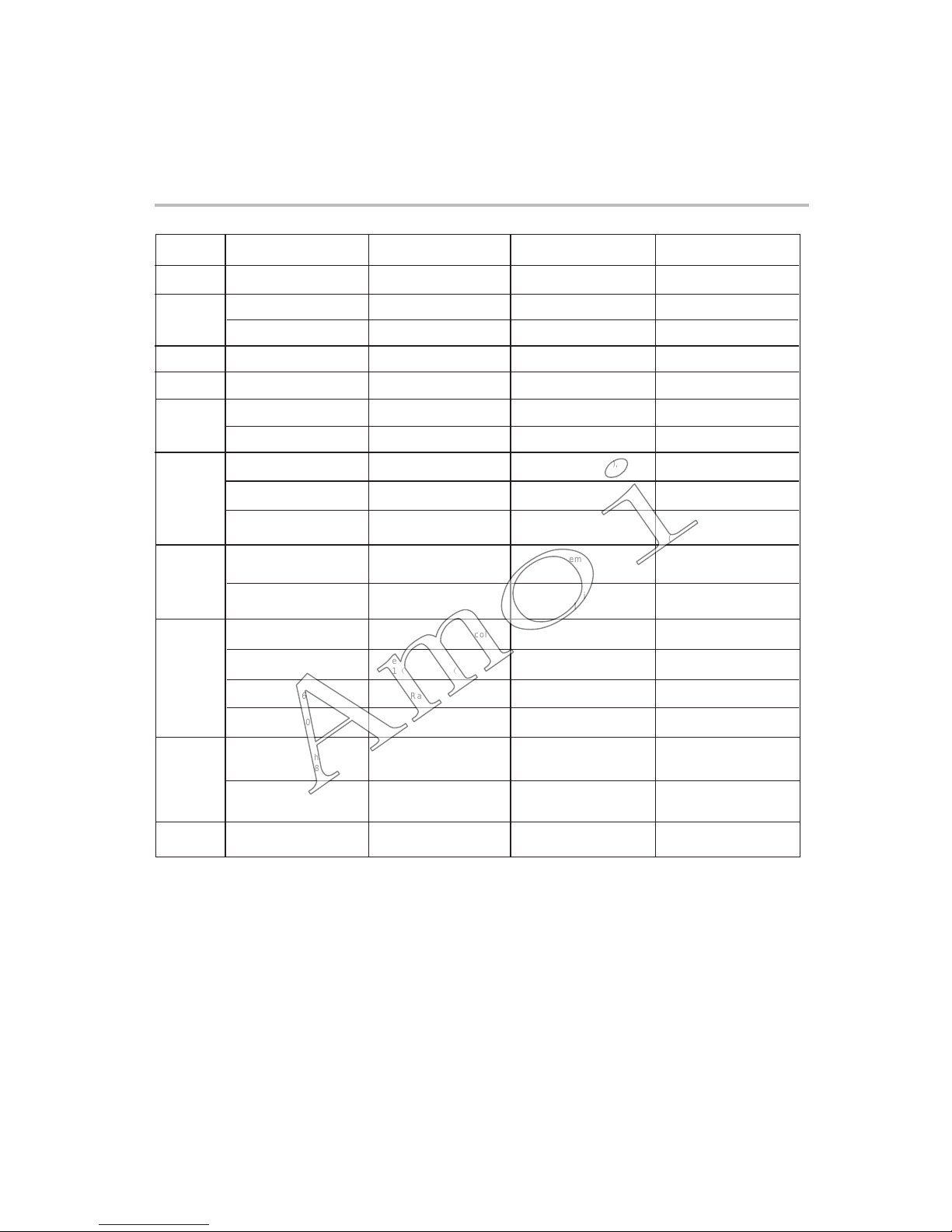
AMOI LC32T1E User manual

Amoi
Service Manual
LCD TV
MODEL:LC26T1E/LC32T1E/LC37T1E/LC42T1E
Notice: Please read this manual and the user’s
manual before repairment. This manual is just for
reference.

After-sales Service manual
Model: LC26T1E/LC32T1E/LC37T1E/LC42T1E
Contents
1.Preparation before maintenance…………………………………………………1
2.Product Specifications……………………………………………………………2
3.Electric connection chart…………………………………………………………3
4.Block diagram of electric ………………………………………………………6
5.Work Principle …………………………………………………………………12
6.Schematic Diagrams……………………………………………………………17
7.Internal Block Diagrams & IC’s ………………………………………………60
8.Software version view and upgrade instruction ………………………………97
9.Exploded Views-Mechanical ………………………………………………104
10.Maintenance spare part list …………………………………………………108
11.Trouble shooting ……………………………………………………………117
Note:Disassembly Instructions
1. Preparation before maintenance: Common contents, it mainly expresses the information
which need your attention, including the Safety instruction and the Protect measure..
2. Electric connection chart: Identify the plug specification and the connection between the
pins and the board by the unit of PCB.
3. Block diagram of electric: Show the signal processing of the unit in the unit of 1C or
circuit.
4. Schematic Diagrams: Provide the circuit chart in the unit of PCB and provide the
detailed principle chart with the simple signal processing and control instruction.
5. Software version view and upgrade instruction: The method of software
version view and the software upgrade instruction.
6. Maintenance spare part list: Including the Package, Accessory, PCB,
Connector, etc. and the material list that the service person can replace
themselves.

1、Preparation before maintenance
1.1、Master basic information.
Adequate communication with customers is required, to learn how the
trouble happens and what the status is. This will help to promote effect and
efficiency of the service.
Learn if the trouble has conflict with technical standards.
1.2、Reappearance of the trouble.
Pleaseassure:
a. If the trouble exists as the customer described, and make initial judgment
of the status, then decide what to do next;
b. If any other trouble exists;
c. May reset the machine under some instances. For example: when
the picture and color could not satisfy the customer, could reset the machine
first and then make amendment. Method: Press the “source”button for about
five seconds, the” Factory setting” will be displayed, select the" factory reset”
and enter, then select the" All Setting( Not include calibration)”and enter.
d. Avoid the worse of trouble during the repair.
1.3、Judgment and Repair
Judge the status of the trouble and find the reason, then repair.
Please cut off the power before disassemble and welding.
Read the manual carefully to learn security attentions.
Please obey the requirement of Disassemble drawing and description strictly ,
use specified screw, take care not to make any scars on the machine especially on the
LCD. Please wear anti-electrostatic gloves when welding. Please review the status
of power, crystal, clock, input and output data. Please read Spare part list if need any
change.
Check the packing material and accessories when change the machine for the
customer.
1

2.Specifications
Environmental
Considerations
Specification
of Monitor
Size
Weight
MODEL
Audio System
TV System
Power Supply
Audio
VGA
Power
Consumption
LC42T1E
Earphone out:
Max.10mW Output
Stereo Jack,32(3.5mm )ΩΦ
Operating Humidity
10%-80% Relative Humidity
:
Audio in: RCAJACK L&R
0.5Vrms (-9dB)
(),
Input:AC 100-240V 50Hz/60Hz
220W
Standby: < 1W
Sync: H/V Separate,
TTL,P.orN.
Video Signal: 0.7Vp-p, 75ohm
Frequency Response:
80Hz-15KHz (at-3dB)
OperatingTemperature:
540℃- ℃
Display Colour 16.7M colours:
PAL, SECAM
BG/ /L/LDK/I '
Pixel Pitch:
0.1615 H 0.4845 V() ()
Aspect Ratio: 16:9
Lamp Life: >=60000H
Unit Dimension(Without stand)
768(H) ×1067(W) ×119(D)mm :
Unit dimension:
823(H) × 1067(W) × 340(D) mm
NOTE: Specifications subject to change without notice. Weight and dimensions are approximate.prior
LC37T1E
Earphone out:
Max.10mW Output
( 3.5mmStereo Jack,32 )ΦΩ
Frequency Response:
80Hz-15KHz (at-3dB)
Operating Humidity
10%-80% Relative Humidity
:
Input:AC 100-240V 50Hz/60Hz
200W
Standby: < 1W
Sync: H/V Separate,
TTL,P.orN.
Video Signal: 0.7Vp-p, 75ohm
Audio in: RCAJACK (L&R),
0.5Vrms (-9dB)
OperatingTemperature:
540℃- ℃
PAL, SECAM
BG/ /L/LDK/I '
Unit Dimension(Without stand)
670(H) × 950(W) ×105(D)mm :
Display Colour 16.7M colours:
Pixel Pitch:
0.426 H 0.426 V() ()
Gross Weight: 32kg
25.5kg
Net Weight:
Gross Weight: 23.5kg
18.5kg
Net Weight: Gross Weight: 36kg
29.5kg
Net Weight:
Gross Weight: 17kg
3.5kg
Net Weight: 1
Unit dimension:
730(H) × 950(W)× 340(D) mm
Aspect Ratio: 16:9
Lamp Life 60000H:>=
Display Colour 16.7M colours:
Pixel Pitch:
0.51 H 0.51 V() ()
Unit dimension:
636(H) ×825(W) × 295(D) mm
Unit dimension(Without stand):
586(H) ×825(W) ×102(D)mm
Aspect Ratio: 16:9
Lamp Life: >=60000H
LC32T1E
Input:AC 100-240V 50Hz/60Hz
150W
PAL, SECAM
Standby: < 1W
BG/ /L/LDK/I '
Sync: H/V Separate,
TTL,P.orN.
Video Signal: 0.7Vp-p, 75ohm
Audio in: RCAJACK (L&R),
0.5Vrms (-9dB)
Earphone out:
Max.10mW Output
3.5 Stereo Jack,32(mm )ΩΦ
Frequency Response:
80Hz-15KHz (at-3dB)
OperatingTemperature:
540℃- ℃
Operating Humidity
10%-80% Relative Humidity
:
Display Colour 16.7M colours:
Pixel Pitch:
0.4215 H 0.4215 V() ()
Unit dimension:
552(H) ×699(W) × 295(D) mm
Unit dimension(Without stand):
512(H) ×699(W) ×98(D)mm
Aspect Ratio: 16:9
Lamp Life: >=60000H
LC26T1E
Input:AC 100-240V 50Hz/60Hz
130W
PAL, SECAM
Standby: < 1W
BG/ /L/LDK/I '
Sync: H/V Separate,
TTL,P.orN.
Video Signal: 0.7Vp-p, 75ohm
Audio in: RCAJACK (L&R),
0.5Vrms (-9dB)
Earphone out:
Max.10mW Output
3.5 Stereo Jack,32(mm )ΩΦ
Frequency Response:
80Hz-15KHz (at-3dB)
OperatingTemperature:
540℃- ℃
Operating Humidity
10%-80% Relative Humidity
2

JV104 4pin updata for TV
JV601
4pin
JV106
16pin
T
osideboard
T
o loudspeakers
J1
8pin
J5
6pin
JF603
To panel
INVERTER BOARD
I/O BOARD
POWER BOARD
SCALER BOARD
J2
10pin
J
V103 10
pin
JV109
10
p
in
T
o tuner
JV402 5pin
Updata for
MCU
JF6
13
p
in
J12
3
p
in
J9
J716
J704
JV101
30
p
in
JV102
30
p
in
J705
J707
HDMI
BOARD
JV404
8pin to key
board
JV403
5pin to IR
board
J
7
0
1
J403
5
p
in
J911
J401
This connect cable only
use in LC37T1E not use
in LC32T1E
3.1、The electric connection chart
connection chart for LC32T1E and LC37T1E
4pin
updata for
TV
3

JV104 4pin updata for TV
JV601
4pin
JV106
16pin
T
os
ide board
T
o loudspeakers
J1
8pin
J5
6pin
JF604
To panel
INVERTER BOARD
I/O BOARD
POWER BOARD
SCALER BOARD
J4
8pin
J
V103 10
pin
JV109
10
p
in
T
o tuner
JV402 5pin
Updata for
MCU
JF6
13
p
in
J12
3
p
in
J9
J716
J704
JV101
30
p
in
JV102
30
p
in
J705
J707
HDMI
BOARD
JV404
8pin to key
board
JV403
5pin to IR
board
J
7
0
1
J403
5
p
in
J911
J401
3.2、The electric connection chart
connection chart for LC42T1E
To INVERTER
4pin
updata
for TV
4

POWER BOARD
3.3 The electric connection chart
INVERTER BOARD
SCALAR BOARD
I/O BOARD
S-I/O
JF6
JF4
JF5
J12 J13
30pin
J14
30pin
J705
J706
JF603
J704
J5
J8
5pin
J9 10pin
TUNER
BOARD
J6
8pin
J31 4pin
For TV updata
J22
For updata MCU
5pin
J33
J32
2pin
2pin
To left speaker
To right speaker
To panel
JF1
POWER
16pin
16pin
J101
J701
4pin
For TV updata
HDMI
Board
J401
J403
50pin
5pin
12pin
12pin
30pin
KEY
BOARD
IR
BOARD
connection chart for LC26T1E
5

4.1.1、The block diagram of POWER
(USE FOR LC32T1E/LC37T1E/LC42T1E)
5VS
+5V
+3.3V
+12V
-12V
+21V
5V_MUTE
+24V
AC
INPUT(90V~264V)
LINE FILTER
U1 ML4800 for
PWM
U3
FS7M0880
U2
FSD200
T11
T12
T4
6

LINE FILTER
U3
FS7M0880 T5
T6
T4
U2
FSD200
S+5V
AC
INPUT(90~264V)
U1
ML4800
+24V
-12V
+12V
+5V
+18V
+3.3V
、
(USE FOR LC26T1E)
7

SCART2 OUT
SCART1-RGB
Form JR1
Form
JV108
Form tuner
Form JR2
RGB
S-RGB
YPbP
r
Y/C
AV-CVBS
SCART2-Y/C
SCART2-CVBS
SCART1-CVBS
AV-CVBS
S1-Y/C
TV-CVBS
4.2、The block diagram of video
U9
PW106
VGA-RGB U1
PI5V330Q U6
AD9885
Digital interface
LCM
HDMI
signal
U11、U12
DDR×2
U13
FLASH
2
9
L
V
1
60
Analog interface
DRAM Microcontroller
and Flash
LVDS OUTPUT
PLL
Group
27M
UV104 filter
circuit
I/O board
UV401
CX2069Q
7--Input 3--Output
Audio/Video Switch
SCART1 OUT
(USE FOR LC32T1E/LC37T1E/LC42T1E)
8

4.3、The block diagram of audio
Loudspeakers
SIF
HDMI-Audio
OUTPUT
SPDIF
Form JR2
HDMI board
AV OUTPUT
AV OUTPUT
Earphone
out
p
ut
Form SCART2
Form SCART1
Form JR2
Form MIC2
AV-Audio
S1-Audio
YPbPr-Audio
HDMI-Audio
AV-Audio
VGA-Audio
S2-Audio
UV401
I/O board
CX2069Q
7-Input 3-Output
Audio/Video
Switch
UV505(I/O board)
TDA9875
Digital TV Sound
Processor. Audio
decoder; control of
volume; switch select of
the input sound
UV502 Two step
filter circuit
UV601 NJW1137
BBE processor
UV602
TPA3100
U101
NJM4556
TO SCART1
TO SCART2
UV103
74HC04
HDMI board TO UV102
U5
WM8761
UV503 Two step
filter circuit
UV504 Two step
filter circuit
UV506 Two step
filter circuit
class-D audio
p
oweram
p
lifie
r
Drive am
p
lifie
r
Form TUNER
(USE FOR LC32T1E/LC37T1E/LC42T1E)
9

U9
PW106B-10L
ImageProcessor
U11
DDR-SDRAM
128M
U12
DDR-SDRAM
128M JF603:
To
LCD
Panel
U13
29LV160CTTC-70
Flash ROM
、
LVDS Signal
J705: From I/O Board
J706: From I/O Board
U15
TDA9875AH
Sound Processor
SIF Signal
Audio
Signal
Control
Signal
I2C
Signal
J704:
From
POWER
Board
POWER:
+5V,+3.3V,+12V
Panel Control Signal: BKLON and ANAPWM
U10
24LC32
EEPROM
I2C
Signal
J401: From HDMI Board
Audio
Signal
Video
and
Control
Signal
U5
WM8761
I2S
Audio
Signal
J403: TO HDMI Board
Power
and
Control
Signal
U27:
COAXIAL_OUT
COAXIAL
Audio
Signal
(USE FOR LC26T1E)
10

U9
PIC16F72ISO
MCU
U6
RX-8025SA
TIME
CONTROLLER
J8: From IR
Board
J6: From KEY
Board
J13: From SCALER Board
J14: From SCALER Board
I2C
Control
For
MCU
U7
CXA2069Q
A/V
SIGNAL
SWITCH
I2C
Control
For
Switch
J12: From Side I/O Board
U15
NJM4558M
Amplifier
Audio
Signal
U17
NJM4558M
Amplifier
U18
NJM4558M
Amplifier
UV9
TPA3100D2
POWER
AMPLIFIER
J32,J33:
To Speaker
J3
RCA
J9:
From TUNER
Board
J11
VGA
U4
74LVC126A
J2
RCA
J1
Update
Interface
J5: From
POWER
Board
CVBS
YC
Video
Audio
Signal
Headphone
Audio VGA: HS and VS
VGA: HS and VS
Video Signal
for VGA
Video
Singal Inputl
Timer
Control
VGA: HS and VS
STB Signal
POWER: S+5V,+5V,
+12V,+18V,-12V
IR
Signal
KEY
Signal
Headphone
Audio
TV
CVBS
Signal
Input
SIF
Signal
Current
Audio
Signal
Audio
Output
YPbPr
Audio
Input
Main
Audio
Signal
Main
Audio
Signal
Main
Audio
Output
I2C
Control
For
TUNER
Update
Control
Signal
、
J17
SCART1
U1
P15V330Q
YPbPr
Video
Input
RGB
Video
Input
SEL
J16
VGA Audio
CVBS
Video
Audio
Signal
J18
SCART2
CVBS
YC
Video
Audio
Signal
CVBS
YC
Video
Signal
TV
CVBS
Signal
Output
U22
NJM4558M
Amplifier
Scart1
Audio
Signal
Scart1
Audio Output
AV
CVBS
Signal
Output
U16
NJM4558M
Amplifier
Scart2
Audio Output
FB1
ASP1
ASP2
(USE FOR LC26T1E)
11

5、Work Principle
The product mainly handles with video signal, such as RF (cable TV),
CVBS(composite video), S-VIDEO(Y/C signal), YPbPr(progressive video), SCART, DTV
signal, VGA and HDMI, as well as audio signal amplifying output. AV includes S-VIDEO
and CVBS. In addition, it can input VGA and other signals to realize PIP function.
Because the product is comprised of three boards, the work principle will separate
into three parts as follows:
5.1、Work Principle of Power Board
1. When power is supplied, whether the TV is turned on or off is decided by the
voltage of STB pin in the mini MCU PIC16F72, the high voltage means standby, and
the low voltage means turning on.
In the standby state, the winding 5 and winding 7 of transformer T4 will supply
5VS voltage after regulated by D13, then the power is fed back to optical coupling,
After regulated by diode D14.the 5VS becomes steady. The circuit combined with
transformer T4 is a standby circuit, RE1 is off, then the power consumption could
be less then 1W. When STB pin in MCU sends out a low voltage order, the RE1 circuit
will work and the two main circuits output 24V、+/-12V,5V,3.3V.
2. When the RE1 is on, the power (90-264VAC) will be transformed into sine wave
by DB2. The C27 will be charged by D3 at first, not by T3, to avoid the C27 charge
saturation, which may cause hardware damages such as MOS JM1 failure.
At the same time, the pin 2、4 of U1 ML4800 will set up current and voltage
for the multiplication organ inside. Then C25 will be charged by R17 and R18,
supplying the power for the pin 13 (VCC) of U1. The PFC circuit begins to work,
PFC circuit includes pin 1, 2, 3, 4, 15, 16, 12 and correlative circuits, pin 13
of U1 (shares the power supply with PWM), pin 14(7.5V reference voltage), pin
7(brae pulse producing circuit, provides switch frequency), together with JM1,
T3 and D8.
When PFC begins to work, the pin 12 output switch waves, opposite to the half
wave sine waves, so when the voltage is highest, the duty cycle is lowest, when
the voltage is lowest, the duty cycle is highest. When JM1 is on, T3 charges, and
when JM1 is off, the stored energy of T3 is released to C27 by the loop circuit
consist of D8, C27, R81, and R83. In this way, the voltage of C27 is stabilized
to 380VDC. feed back by the 15 pin of U1. R26, R27 and R23 compose the voltage
dividing resistances. After dividing, the voltage of R23 reaches 2.5V.There is
a 2.5V exact voltage source inside the pin 15. Comparing with it, equation means
the voltage reaches 380V steadily. If the voltage of C27 is lower than 380V, then
the voltage of R23 will be lower than 2.5V. Compared with of 2.5V voltage, pin
16 will output high voltage, making the duty cycle of pin 12 higher, then the
energy storage of T3 increases, and voltage of C27 is higher. Contrarily, the
voltage of C27 is lower.
The pin 3 of U1 4800 is the detecting pin for PFC average voltage mode. The
minus voltage peak value on the pin 3 by R81 should not exceed 1V. Otherwise, the
12

current is limited, and the 380V voltage of PFC will descend. Actually, the current
is limited when the peak value of this board is 0.7V. The pin 4 is a line voltage
detecting pin. It detects the input AC Voltage, and when the 264V voltage becomes
lower to about 80V, the amplifying ratio of the 4th pin is higher, and the duty
cycle of the pin 12 of FPC is higher, the current to the PFC is higher. So when
the input voltage decreases, the power output to C27 will not change. The pin 2
is power detecting pin. The purpose of this pin is:
1) It tries to make the frequency and phase of PFC switch current envelopment
same with input voltage’s, so the PF is close to 1 and the resonance waves are
smallest;
2) It decreases when the duty cycle of PFC increases, increases when detecting
current decreases.
3. When the TV is turned on and the PFC voltage of C27 reaches 380V 2-3%, the
switching power supply PWM begins to work, pin 5 of 4800 is turned on and begins
to charge, when charges to 0.7V, the PWM circuit begins to work, the duty cycle
of PWM cannot exceed 50% when stimulating positively, therefore the duty cycle
of 4800 is limited to 48%, in order to protect switching power. After this, pin
11 output switch pulse signal, makes the transformer T11 work. After rectificated
by D15, pin 6 and pin 7 of the transformer T11 provide a voltage supply, which
is between 13V and 17.5V. To pin 13 (VCC) of 4800, this positive stimulating
transformer just transform voltage. After rectificated by D16, T8 begins to store
energy, C49 filters and outputs 24V,
The 24V voltage regulation process is: 24V provides 2.5V voltage by voltage
division circuit made of R42、R43,then inputs 2.5V to U6, in TVL431, compares
with the internal norm voltage regulation source, when 24V output voltage is low,
U6 pulls down U5 light coupling voltage ,which pulls down the voltage of pin 6
in 4,800 accordingly, increases duty cycle of the pin 11(PWM), so the 24V output
power increases, resulting in the rising of 24V. Contrarily, it drops down.
There is another FS7M0880 switching power supply, when PFC voltage 380V rises,
pin 3(VCC) of U3 FS7M0880 begins to charge by R65, when VCC reaches 13 - 16V,
pin 5 electric capacity begins to charge and to work. Pin 5 and pin 6 of T12 output
voltage accordingly, supplies the power for VCC, the T11 output 5V, +/-12V voltage.
This switching power supply is regulated from 5V; the voltage regulation process
is the same with 24V’s.
5.2、Work Principle of SCALER board
1、SCALER board can: process all video signals; provide the display format which
is accordance with PANEL requirement; finish OSD display and menu operation;
communicate with mini MCU on IO board to receive the key signal and handle
correspondingly.
2、 Features of SCALER board:
The core of SCALER board is single chip PW106. After the outer signal enters
PW106, it is all up to this chip to finish the video decoding of all formats and
picture processing, and finally provide the PANEL-required display format and
13

switch into LVDS signal to send it to PANEL for processing.
3、flow of main video signal process:
CVBS composite video signal of TUNER (including TUNER signal) and S-VIDEO signal
is output to PW106 of SCALER board via 2069 of IO board.
PW106 handles with the input video signal, such as resolution and field switch,
OSD overlapping, multi-window handling, to switch into PANEL-required resolution.
And LVDS channel transports the picture data to PANEL and finally the correct
picture is displayed on PANEL.
It should be noted that PW106 outputs analog video signal and the main transport
mode is difference transport mode. Therefore, when maintenance, not only‘+’
signal but also ‘-’signal of all video channels should be checked.
4、Flow of audio signal process:
Most of audio signals are processed on I/O board, while SCALER board only
processes the audio signal from HDMI. Because HDMI accepts the HD digital signal
input, its audio input should be digital signal, which is switched into analog audio
signal via WM8761. Then the processed analog audio signal is sent to IO board for
amplifying.
5、Flow of main system program
The loading program of PW106 is saved in the 8M flash chip. If the flash chip
is destroyed, TV can’t be powered on and logo can’t be displayed.
The program upgrading of FLASH can be done via the upgrading port of SCALER
board or IO board, as long as the power supply and FLASH and PW106 are normal.
It has nothing to do with DDR chip.
The running of PW106 depends on two DDR chips. If part of DDR circuit is
abnormal, then TV can be powered on and logo can be displayed, but TV doesn’t accept
any IR order once logo disappears.
6、Some other controls
For LCD PANEL, besides PW106 transporting LVDS signal to PANEL, it also: 1/.
suppliers power (LVDSVDD)to signal port of PANEL. The voltage is 5V or 12V,
which is up to the PANEL requirement; 2/. Controls the backlight of PANEL:
BKL-ON/OFF,which controls the On/Off of backlight of PANEL(above 1V=On,below
1V=Off),while BRT-ADJ controls the brightness of backlight.
When TV can’t display, it should be checked first if the backlight is on. If the
backlight is on, then check if LVDSVDD has voltage. If no voltage, then it is the
reason that the drive tube of voltage is destroyed. If LVDSVDD is OK, then please
check LVDS cable.
PW106 checks the status of earphone socket. When the earphone is inserted into
the earphone socket, the EAR-INT signal sent to PW106 will be high level. Then ,
PW106 will low down STANDBY signal, which connect the signal of control end of
amplifier chip LX1722. When the STANDBY signal is high level, then amplifier works;
otherwise, the amplifier enters the standby mode.
It should be noted that sometimes if the connector between mini I/O board and IO
board is lax or pulled off, then EAR-INT will be high level and speaker has no
voice output. Therefore, if maintain the TV with no-voice-output speaker, please
14

check if the EAR-INT signal is abnormal, which is in order to avoid wasting time
on checking amplifier.
Regarding the connecting with IO board, it is important that I2C signal
connects with MCU (MCU-INT、SCL-MCU、SDA-MCU). If there is any problem with
the connecting, then the key and remote control work out.
5.3、Work Principle of I/O board
1、I/O board mainly: inputs & outputs AV signal, switches audio and video,
amplifies audio, control mini MCU and process key.
2、I/O board can be divided into three modules, a)audio module,to process,
switch and amplify audio;b)video module, to input & output video switch;c)
mini MCU module. When maintenance, if no sound, then the audio module has problem;
if no picture, then the video module has problem; if the remote control and keys
work out, then the MCU module has problem under the circumstance that IR&KEY board
is OK.
a)Audio module:is divided into small signal process and power amplification.
Small signal can be separated into: left & right audio analog signal. Analog audio
signal enters CX2069Q(UV401) via the following 7 channels: left & right audio
channels of AV2(S-VIDEO2), left & right audio signals of SCART1 & SCART2,
left & right signals of YPbPr,left & right signals of VGA,left & right audio
signals of HDMI sent by SCALER board and the audio signal switched from digital
TUNER. The above audio signals are switched via CXA2069Q,and sent together with
SIF signal from DVB board to TDA9875(UV505) for processing. TDA9875(UV505)
mainly decoding the audio channel of SIF signal and control the volume. After
processed by the chip, 4 routes of L & R signals are output from the output end
of the chip. Among them, two routes are output from SCART1 & SCART2 after filtered
by filter web; one is output from earphone after filtered and amplified by NJM4556;
the last one is output by speaker after processed by NJW1137(UV601)and amplified
by TPA3100(UV602).
During the whole process, UV401, UV601 and UV505 are controlled by I2C. If
the audio trouble is caused by UV401 and UV601, connect the signal via lead from
the input end of chip to output end to judge if the work is normal. If the video
trouble is caused by UV401, please judge in the same way. In the whole audio
channel, if audio output is normal, then MUTE signal is low level, otherwise,
high level.
b)Video module:four routes CVBS, one route S-VIDEO, one route RGB signal
and one route TV-CVBS signal. After switched by CXA2069Q(UV401), one route CVBS,
one route S-VIDEO and one route RGB are input to the corresponding analog input
ports of PW106 of SCALER board respectively. In addition, the YPbPr signal of I/O
board input into the corresponding analog input port of PW106. The last route is
VGA and HDMI. HDMI is directly input to the digital port of PW106, and the input
VGA signal is sent to PI5V330Q(U1) and separated into two routes: one is input
from the analog port of PW106, while one is input from the digital port of PW106
after switched by AD9985(U6) into digital signal. In this way, PIP function can
15

be realized by one video IC.
c)Mini MCU module:remote and key signals receiving. The remote and key
signal receiving is dependent, but the processing modes in MCU are the same. If
the remote control and key both work out, then judge if the power supply and
peripheral circuit of MCU is normal. If only one works out, check if PIN21 of U202
IR or PIN26-28 has signal input.
16

6.1.Schematic Diagrams
Scaler and I/O part for LC26T1E
17

18
This manual suits for next models
3
Table of contents
Other AMOI LCD TV manuals