Ampak AP6356SD Series User manual

AMPAK Technology Inc. www.ampak.com.tw Proprietary & Confidential Information i
Doc. NO:
AMPAK
AP6356SDXX
Evaluation Kits
User manual
Version 1.0
Revision History
Date
Revision Content
Revised By
Version
2015/12/28
Initial released
Aron
1.0

Federal Communication Commission Interference Statement
This device complies with Part 15 of the FCC Rules. Operation is subject to
the following two conditions: (1) This device may not cause harmful
interference, and (2) this device must accept any interference received,
including interference that may cause undesired operation.
This equipment has been tested and found to comply with the limits for a
Class B digital device, pursuant to Part 15 of the FCC Rules. These limits
are designed to provide reasonable protection against harmful interference in a
residential installation. This equipment generates, uses and can radiate radio
frequency energy and, if not installed and used in accordance with the
instructions, may cause harmful interference to radio communications.
However, there is no guarantee that interference will not occur in a particular
installation. If this equipment does cause harmful interference to radio or
television reception, which can be determined by turning the equipment off
and on, the user is encouraged to try to correct the interference by one of the
following measures:
- Reorient or relocate the receiving antenna.
- Increase the separation between the equipment and receiver.
- Connect the equipment into an outlet on a circuit different from that
to which the receiver is connected.
- Consult the dealer or an experienced radio/TV technician for help.
FCC Caution: Any changes or modifications not expressly approved by the
party responsible for compliance could void the user's authority to operate this
equipment.
This transmitter must not be co-located or operating in conjunction with any
other antenna or transmitter.

Radiation Exposure Statement:
The product comply with the FCC portable RF exposure limit set forth for an
uncontrolled environment and are safe for intended operation as described in
this manual. The further RF exposure reduction can be achieved if the product
can be kept as far as possible from the user body or set the device to lower
output power if such function is available.
This device is intended only for OEM integrators under the following conditions:
1) The transmitter module may not be co-located with any other transmitter
or antenna.
As long as 2conditions above are met, further transmitter test will not be
required. However, the OEM integrator is still responsible for testing their
end-product for any additional compliance requirements required with this
module installed
IMPORTANT NOTE: In the event that these conditions can not be met (for
example certain laptop configurations or co-location with another transmitter),
then the FCC authorization is no longer considered valid and the FCC ID can
not be used on the final product. In these circumstances, the OEM integrator
will be responsible for re-evaluating the end product (including the transmitter)
and obtaining a separate FCC authorization.
End Product Labeling
The product can be kept as far as possible from the user body or set the device
to lower output power if such function is available. The final end product must
be labeled in a visible area with the following: “Contains FCC
ID:ZQ6-AP6356SDXX”. The grantee's FCC ID can be used only when all
FCC compliance requirements are met.
Manual Information To the End User
The OEM integrator has to be aware not to provide information to the end user
regarding how to install or remove this RF module in the user’s manual of the
end product which integrates this module.
The end user manual shall include all required regulatory information/warning
as show in this manual.

Industry Canada statement:
This device complies with ISED’s licence-exempt RSSs. Operation is subject to the
following two conditions: (1) This device may not cause harmful interference, and (2)
this device must accept any interference received, including interference that may
cause undesired operation.
Le présent appareil est conforme aux CNR d’ ISED applicables aux appareils radio
exempts de licence. L’exploitation est autorisée aux deux conditions suivantes : (1) le
dispositif ne doit pas produire de brouillage préjudiciable, et (2) ce dispositif doit
accepter tout brouillage reçu, y compris un brouillage susceptible de provoquer un
fonctionnement indésirable.
Radiation Exposure Statement:
The product comply with the Canada portable RF exposure limit set forth for an
uncontrolled environment and are safe for intended operation as described in this
manual. The further RF exposure reduction can be achieved if the product can be kept
as far as possible from the user body or set the device to lower output power if such
function is available.
Déclaration d'exposition aux radiations:
Le produit est conforme aux limites d'exposition pour les appareils portables RF pour
les Etats-Unis et le Canada établies pour un environnement non contrôlé.
Le produit est sûr pour un fonctionnement tel que décrit dans ce manuel. La réduction
aux expositions RF peut être augmentée si l'appareil peut être conservé aussi loin que
possible du corps de l'utilisateur ou que le dispositif est réglé sur la puissance de sortie
la plus faible si une telle fonction est disponible.
This device is intended only for OEM integrators under the following conditions: (For
module device use)
1) The transmitter module may not be co-located with any other transmitter or
antenna.
As long as 2conditions above are met, further transmitter test will not be required.
However, the OEM integrator is still responsible for testing their end-product for any
additional compliance requirements required with this module installed.
Cet appareil est conçu uniquement pour les intégrateurs OEM dans les conditions
suivantes: (Pour utilisation de dispositif module)

1) Le module émetteur peut ne pas être coïmplanté avec un autre émetteur ou antenne.
Tant que les 2conditions ci-dessus sont remplies, des essais supplémentaires sur
l'émetteur ne seront pas nécessaires. Toutefois, l'intégrateur OEM est toujours
responsable des essais sur son produit final pour toutes exigences de conformité
supplémentaires requis pour ce module installé.
IMPORTANT NOTE:
In the event that these conditions can not be met (for example certain laptop
configurations or co-location with another transmitter), then the Canada authorization
is no longer considered valid and the IC ID can not be used on the final product. In
these circumstances, the OEM integrator will be responsible for re-evaluating the end
product (including the transmitter) and obtaining a separate Canada authorization.
NOTE IMPORTANTE:
Dans le cas où ces conditions ne peuvent être satisfaites (par exemple pour certaines
configurations d'ordinateur portable ou de certaines co-localisation avec un autre
émetteur), l'autorisation du Canada n'est plus considéré comme valide et l'ID IC ne
peut pas être utilisé sur le produit final. Dans ces circonstances, l'intégrateur OEM
sera chargé de réévaluer le produit final (y compris l'émetteur) et l'obtention d'une
autorisation distincte au Canada.
End Product Labeling
The product can be kept as far as possible from the user body or set the device to
lower output power if such function is available. The final end product must be
labeled in a visible area with the following: “Contains IC: ”.
Plaque signalétique du produit final
L'appareil peut être conservé aussi loin que possible du corps de l'utilisateur ou que le
dispositif est réglé sur la puissance de sortie la plus faible si une telle fonction est
disponible. Le produit final doit être étiqueté dans un endroit visible avec l'inscription
suivante: "Contient des IC: ".
Manual Information To the End User
The OEM integrator has to be aware not to provide information to the end user
regarding how to install or remove this RF module in the user’s manual of the end
product which integrates this module.

The end user manual shall include all required regulatory information/warning as
show in this manual.
Manuel d'information à l'utilisateur final
L'intégrateur OEM doit être conscient de ne pas fournir des informations à l'utilisateur
final quant à la façon d'installer ou de supprimer ce module RF dans le manuel de
l'utilisateur du produit final qui intègre ce module.
Le manuel de l'utilisateur final doit inclure toutes les informations réglementaires
requises et avertissements comme indiquédans ce manuel.
Caution :
(i) the device for operation in the band 5150-5250 MHz is only for indoor use to
reduce the potential for harmful interference to co-channel mobile satellite systems;
(ii) the maximum antenna gain permitted for devices in the bands 5250-5350 MHz
and 5470-5725 MHz shall be such that the equipment still complies with the e.i.r.p.
limit;
(iii) the maximum antenna gain permitted for devices in the band 5725-5850 MHz
shall be such that the equipment still complies with the e.i.r.p. limits specified for
point-to-point and non-point-to-point operation as appropriate; and
(iv) the worst-case tilt angle(s) necessary to remain compliant with the e.i.r.p. elevation
mask requirement set forth in Section 6.2.2(3) shall be clearly indicated.
(v) Users should also be advised that high-power radars are allocated as primary users
(i.e. priority users) of the bands 5250-5350 MHz and 5650-5850 MHz and that these
radars could cause interference and/or damage to LE-LAN devices.
Avertissement:
Le guide d’utilisation des dispositifs pour réseaux locaux doit inclure des instructions
précises sur les restrictions susmentionnées, notamment :
(i) les dispositifs fonctionnant dans la bande 5150-5250 MHz sont réservés
uniquement pour une utilisation à l’intérieur afin de réduire les risques de brouillage
préjudiciable aux systèmes de satellites mobiles utilisant les mêmes canaux;
(ii) le gain maximal d'antenne permis pour les dispositifs utilisant les bandes de 5250 à 5

350 MHz et de 5470 à 5725 MHz doit être conforme à la limite de la p.i.r.e;
(iii) le gain maximal d'antenne permis (pour les dispositifs utilisant la bande de 5 725 à 5
850 MHz) doit être conforme à la limite de la p.i.r.e. spécifiée pour l'exploitation point à
point et l’exploitation non point à point, selon le cas;
(iv) les pires angles d’inclinaison nécessaires pour rester conforme à l’exigence de la
p.i.r.e. applicable au masque d’élévation, et énoncée à la section 6.2.2 3), doivent être
clairement indiqués.
(v) De plus, les utilisateurs devraient aussi être avisés que les utilisateurs de radars de
haute puissance sont désignés utilisateurs principaux (c.-à-d., qu’ils ont la priorité)
pour les bandes 5250-5350 MHz et 5650-5850 MHz et que ces radars pourraient
causer du brouillage et/ou des dommages aux dispositifs LAN-EL.

第十二條 經型式認證合格之低功率射頻電機,非經許可,公司、商號或使用者均
不得擅自變更頻率、加大功率或變更原設計之特性及功能。
第十四條 低功率射頻電機之使用不得影響飛航安全及干擾合法通信;經發現有干
擾現象時,應立即停用,並改善至無干擾時方得繼續使用。
前項合法通信,指依電信法規定作業之無線電通信。
低功率射頻電機須忍受合法通信或工業、科學及醫療用電波輻射性電機設
備之干擾。
1. 本模組於取得認證後將依規定於模組本體標示審驗合格標籤。
2. 系統廠商應於平台上標示「本產品內含射頻模組:XXXyyyLPDzzzz-x」字 樣 。

AMPAK Technology Inc. www.ampak.com.tw Proprietary & Confidential Information
Doc. NO:
3
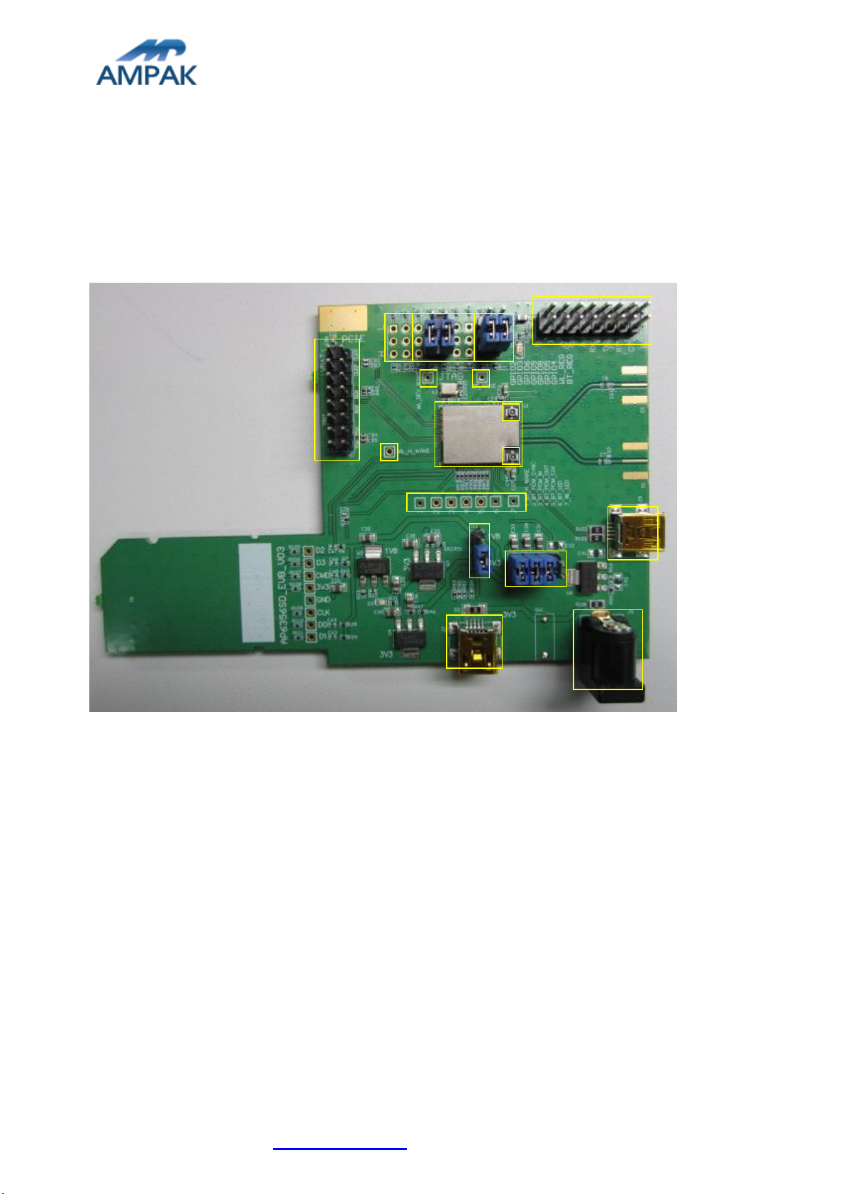
1. AP6356SDXX Evaluation Board Introduction
AP6356SDXX Evaluation board (EVB) likes as figure1. That is designed for IEEE802.11
a/b/g/n/ac 2x2 WLAN with integrated Bluetooth. It is subject to provide a convenient
environment for customer’s verification on WiFi or Bluetooth function. There are many
controller pins and reserved GPIO on Evaluation board which describes as below.
Figure1. Top view of AP6356SDXX EVB
Interface highlights:
1. U1: AP6356SDXX SIP module.
2. J1: UART interface connects with UART transport board for BT.
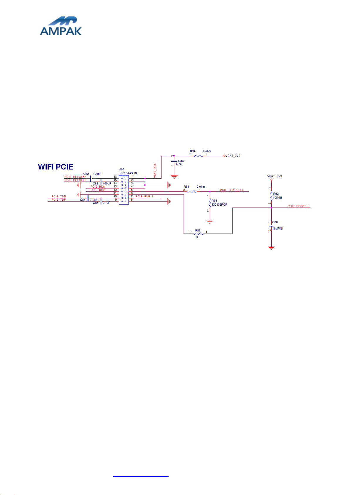
3. J80: PCIE interface connects with PCIE transport board for WIFI.
4. J3: Enable(H) or disable(L) Bluetooth and WiFi function.
5. J4: PCIE interface strapping option
6. J5: 5V DC adaptor input connector.
7. J6: 3V3 RF/ VBAT / WL_VIO / BT_VIO for main system I/O power path.
8. J7/J9: 5V DC mini USB input connector.
9. J10: GPIO_2 (input/output) and GPIO_3 (input/output)
10.J11: WL_VIO power path for 1V8 or 3V3 selection.
11.A1: I-PEX connector let RF signal in/out path, you could connect with RF cable or
J10
J4
J3
J1
A2
U1
A1
J80
ct2
ct3
ct4
J7
J5
J9
J11
J6
ct1

AMPAK Technology Inc. www.ampak.com.tw Proprietary & Confidential Information
Doc. NO:
4
Dipole antenna.
12.A2: I-PEX connector let RF signal in/out path, you could connect with RF cable or
Dipole antenna.
13.Ct1-Ct4: WLAN and BT control pins, strongly recommended WL_H_WAKE(IRQ)
connected to MCU.
2. WiFi function verification step
WIFI PCIe: PCIe interface definition as below J80 dip connector and this should be used
3.3V for PCIe voltage.
Figure3. WiFi verification connection interface to Host PCIE
Hardware Setup:
Refer to Figure3 PCIE pin definition connects the J80 interface of
AP6356SDXX evaluation board to Host PCIE control interface.
Connects an external antenna at I-PEX connector on the evaluation board.
Note to the VDDIO voltage level should be the same with GPIO voltage level of
Host CPU. (VDDIO 3.3V or 1.8V selection by jump J11)
Pull High J4 are necessary .
WiFi software setup:
Please follow up software guideline of Ampak official released.

AMPAK Technology Inc. www.ampak.com.tw Proprietary & Confidential Information
Doc. NO:
5
3. Bluetooth function verification step
UART:
Figure4. Bluetooth verification connection interface to Host UART
Hardware Setup:
Refer to Figure4 UART pin definition connects the J1 interface of AP6356SDXX
evaluation board to Host UART control interface.
Connects an external antenna at I-PEX connector on the evaluation board.
Note to the VDDIO voltage level should be the same as GPIO voltage level of
Host CPU.
USB:
Figure5. Bluetooth verification connection interface to Host USB

AMPAK Technology Inc. www.ampak.com.tw Proprietary & Confidential Information
Doc. NO:
6
Hardware Setup:
Refer to Figure5 USB pin definition connects the J9 interface of AP6356SDXX
evaluation board to Host USB control interface.
Connects an external antenna at I-PEX connector on the evaluation board.
WiFi and Bluetooth software setup:
Please follow up software guideline of Ampak official released.

AMPAK Technology Inc. www.ampak.com.tw Proprietary & Confidential Information
Doc. NO:
正基科技股份有限公司
SPECIFICATION
SPEC. NO.:REV:1.6
DATE:09. 07.2015
PRODUCT NAME:AP6356SDXX
Customer APPROVED
Company
Representative
Signature
PREPARED
REVIEW
APPROVED
DCC ISSUE
PM
QA

AMPAK Technology Inc. www.ampak.com.tw Proprietary & Confidential Information
Doc. NO:
AMPAK
AP6356SDXX
2x2 WiFi + Bluetooth4.1
Module Spec Sheet

AMPAK Technology Inc. www.ampak.com.tw Proprietary & Confidential Information
Doc. NO:
1
Revision History
Date
Revision Content
Revised By
Version
2014/09/25
-Preliminary
Brian
1.0
2014/10/26
-Pin definition modified
Brian
1.1
2014/12/11
-Pin definition modified
Brian
1.2
2015/03/18
-Layout and Bluetooth Spec modified
- Pin map and physical dimension modified
Dora
1.3
2015/05/12
-Add Part Number Description
Dora
1.4
2015/06/29
-Add Packet type and total pins
Dora
1.5
2015/09/07
-Modify label quantity and MSL
Dora
1.6

AMPAK Technology Inc. www.ampak.com.tw Proprietary & Confidential Information
Doc. NO:
2
Contents
Contents ...................................................................................................................2
1. Introduction.........................................................................................................4
2. Features............................................................................................................... 5
3. Deliverables ........................................................................................................6
3.1 Deliverables....................................................................................................6
3.2 Regulatory certifications .................................................................................6
4. General Specification......................................................................................... 7
4.1 General Specification......................................................................................7
4.2 Voltages..........................................................................................................7
4.2.1 Absolute Maximum Ratings....................................................................7
4.2.2 Recommended Operating Rating...........................................................7
5. WiFi RF Specification.........................................................................................8
5.1 2.4GHz RF Specification.................................................................................8
5.2 5GHz RF Specification............................................................................... 11
6. Bluetooth Specification.................................................................................... 16
6.1 Bluetooth Specification ................................................................................. 16
7. Pin Assignments............................................................................................... 17
7.1 Pin Map ........................................................................................................ 17
7.2 Pin Definition ................................................................................................17
8. Dimensions....................................................................................................... 21
8.1 Physical Dimensions ....................................................................................21
8.2 Layout Recommendation..............................................................................22
8.3 Part Number Description .............................................................................. 23
9. External clock reference.................................................................................. 24
9.1 SDIO Pin Description....................................................................................24
10.Host Interface Timing Diagram........................................................................ 25
10.1 Power-up Sequence Timing Diagram.........................................................25
10.2 SDIO Default Mode Timing Diagram........................................................... 27
10.3 SDIO High Speed Mode Timing Diagram ................................................... 28
10.4 SDIO Bus Timing Specifications in SDR Modes......................................... 29
10.5 SDIO Bus Timing Specifications in DDR50 Mode.......................................31
11.Recommended Reflow Profile......................................................................... 32
12. Package Information........................................................................................ 33
12.1Label............................................................................................................ 33
Label CInner box label . .................................................................................... 33
Label DCarton box label . ................................................................................. 33
12.2 Dimension................................................................................................... 34

AMPAK Technology Inc. www.ampak.com.tw Proprietary & Confidential Information
Doc. NO:
4
1. Introduction
AMPAK Technology would like to announce a low-cost and low-power consumption module
which has all of the WiFi and Bluetooth functionalities. The highly integrated module makes
the possibilities of web browsing, VoIP, Bluetooth headsets applications. With seamless
roaming capabilities and advanced security, also could interact with different vendors’
802.11a/b/g/n/ac 2x2 Access Points in the wireless LAN.
The wireless module complies with IEEE 802.11 a/b/g/n/ac 2x2 MIMO standard and it can
achieve up to a speed of 867Mbps with dual stream in 802.11n to connect the wireless LAN.
The integrated module provides SDIO/PCIe interface for WiFi,UART / USB/ PCM interface
for Bluetooth.
This compact module is a total solution for a combination of WiFi + BT technologies. The
module is specifically developed for Smart phones and Portable devices.

AMPAK Technology Inc. www.ampak.com.tw Proprietary & Confidential Information
Doc. NO:
5
2. Features
Lead Free design which is compliant with ROHS requirements.
802.11a/b/g/n/ac dual-band radio with virtual-simultaneous dual-band operation
Dual-stream spatial multiplexing up to 867 Mbps data rate.
Supports 20, 40, 80 MHz channels with optional SGI(256 QAM modulation)
Supports IEEE 802.11 ac/n beam forming.
Supports IEEE 802.15.2 external coexistence interface to optimize bandwidth utilization
with other co-located wireless technologies such as LTE, GPS, or WiMAX.
- Supports standard SDIO/PCIe interfaces.
BT host digital interface:
- HCI UART (up to 4 Mbps)
- PCM for audio data
Complies with Bluetooth Core Specification Version 4.1 with provisions for supporting
future specifications. With Bluetooth Class1 or Class2 transmitter operation.
Supports extended synchronous connections (eSCO), for enhanced voice quality by
allowing for retransmission of dropped packets.
Adaptive frequency hopping (AFH) for reducing radio frequency interference.
A simplified block diagram of the module is depicted in the figure below.
Switch
UART
PCM/I2S
RTC_CLK 32.768KHz
Ref_CLK
Discrete
BT
WLAN
WLAN
Switch
Discrete
VBAT
VDDIO
USB
PCIe

AMPAK Technology Inc. www.ampak.com.tw Proprietary & Confidential Information
Doc. NO:
6
3. Deliverables
3.1 Deliverables
The following products and software will be part of the product.
Module with packaging
Evaluation Kits
Software utility for integration, performance test.
Product Datasheet.
Agency certified pre-tested report with the adapter board.
3.2 Regulatory certifications
The product delivery is a pre-tested module, without the module level certification. For
module approval, the platform’s antennas are required for the certification.
Table of contents
Other Ampak Motherboard manuals