Analog Technologies AHVAN2R5KV20MA User manual

1161 Ringwood Ct, #110, San Jose, CA 95131, U. S. A. Tel.: (408) 748-9100, Fax: (408) 770-9187 www.analogtechnologies.com
Copyrights 2000-2023, Analog Technologies, Inc. All Rights Reserved. Updated on 7/20/2023 Email: [email protected]/[email protected]m 1
A
nalog Technologies AHVAN2R5KV20MA
High Voltage Amplifier/Piezo Driver
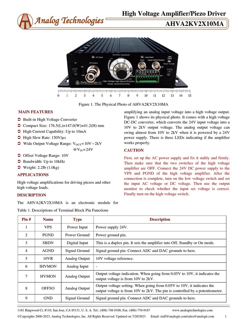
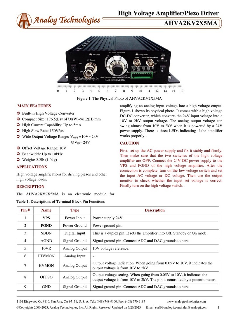
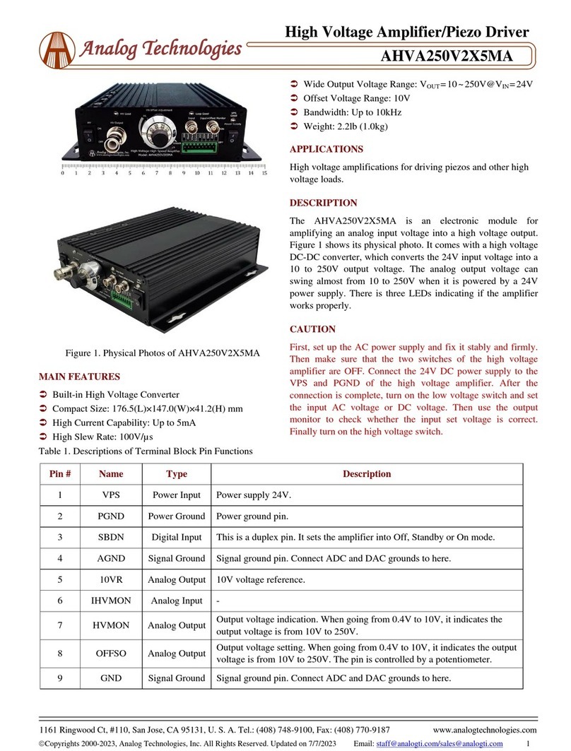
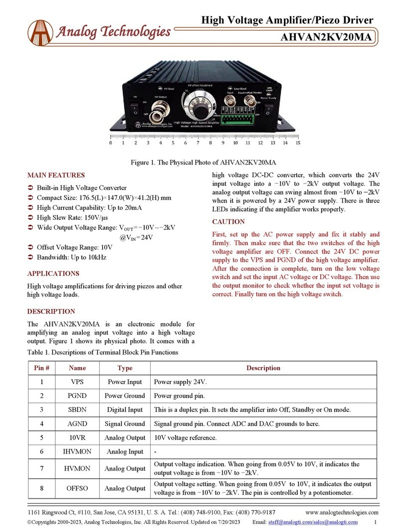
Figure 1. The Physical Photo of AHVAN2R5KV20MA
MAIN FEATURES
Built-in High Voltage Converter
Compact Size: 176.5(L)×147.0(W)×41.2(H) mm
High Current Capability: Up to 20mA
High Slew Rate: 150V/µs
Wide Output Voltage Range:
VOUT =−10V ~−2.5kV@VIN =24V
Offset Voltage Range: 10V
Bandwidth: Up to 10kHz
APPLICATIONS
High voltage amplifications for driving piezos and other
high voltage loads.
DESCRIPTION
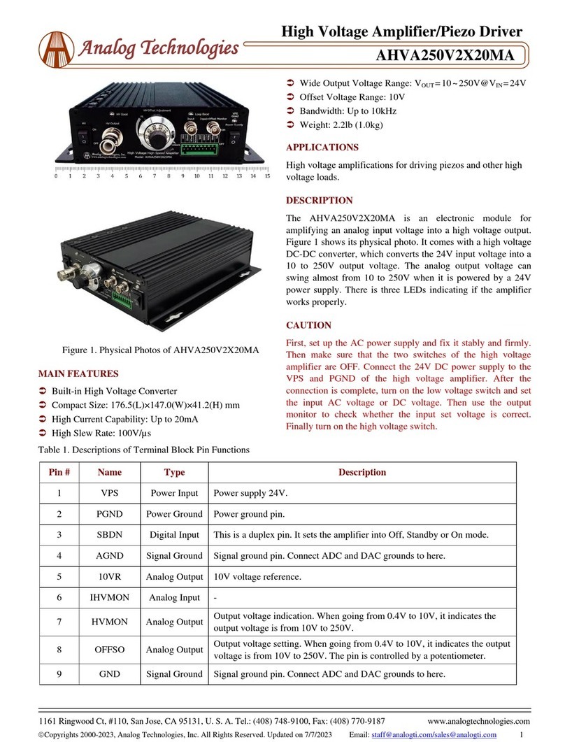
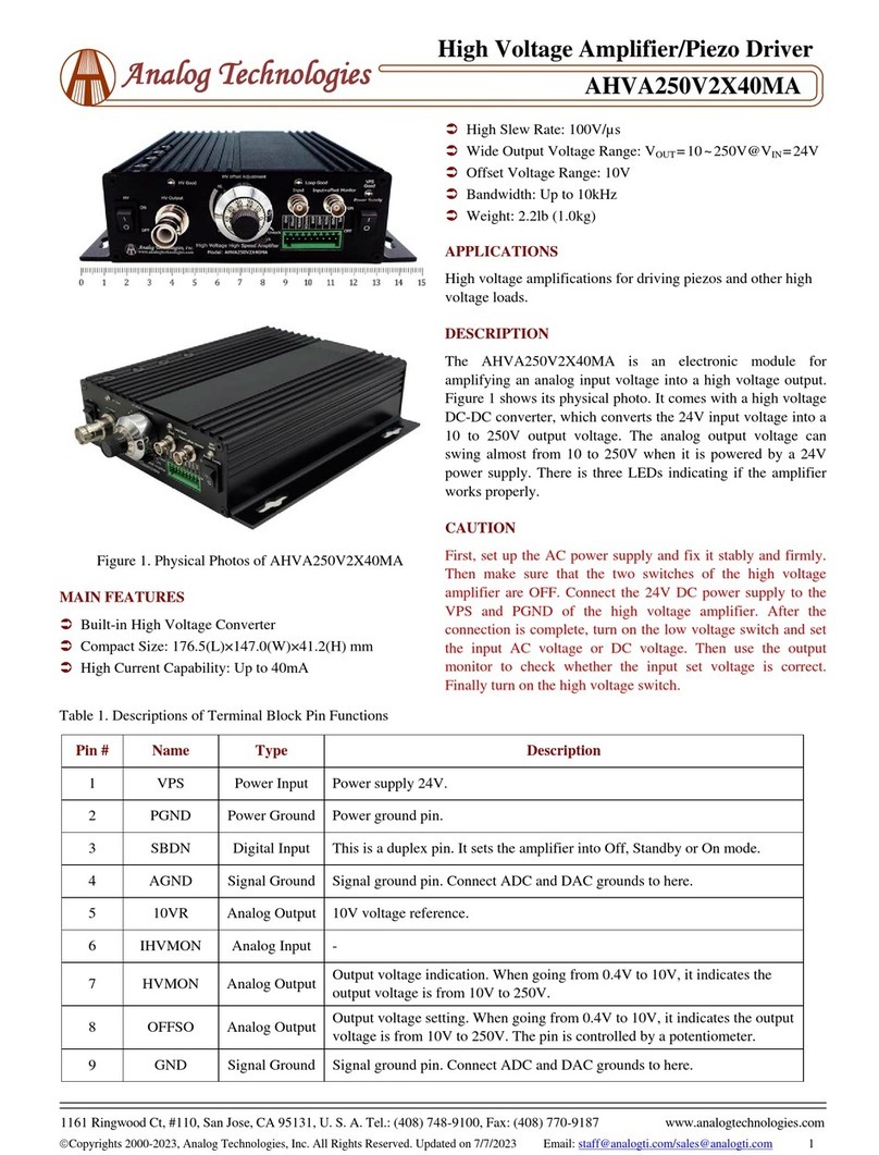
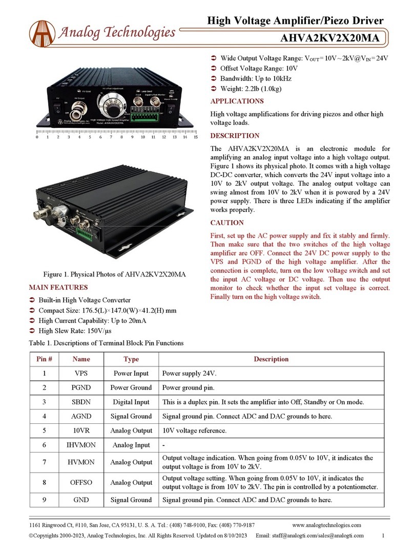
The AHVAN2R5KV20MA is an electronic module for
amplifying an analog input voltage into a high voltage output.
Figure 1 shows its physical photo. It comes with a high voltage
DC-DC converter, which converts the 24V input voltage into a
−10V to −2.5kV output voltage. The analog output voltage can
swing almost from −10V to −2.5kV when it is powered by a
24V power supply. There is three LEDs indicating if the
amplifier works properly.
CAUTION
First, set up the AC power supply and fix it stably and firmly.
Then make sure that the two switches of the high voltage
amplifier are OFF. Connect the 24V DC power supply to the
VPS and PGND of the high voltage amplifier. After the
connection is complete, turn on the low voltage switch and set
the input AC voltage or DC voltage. Then use the output
monitor to check whether the input set voltage is correct.
Finally turn on the high voltage switch.
Table 1. Descriptions of Terminal Block Pin Functions
Pin # Name Type Description
1 VPS Power Input Power supply 24V.
2 PGND Power Ground Power ground pin.
3 SBDN Digital Input This is a duplex pin. It sets the amplifier into Off, Standby or On mode.
4 AGND Signal Ground Signal ground pin. Connect ADC and DAC grounds to here.
5 10VR Analog Output 10V voltage reference.

1161 Ringwood Ct, #110, San Jose, CA 95131, U. S. A. Tel.: (408) 748-9100, Fax: (408) 770-9187 www.analogtechnologies.com
Copyrights 2000-2023, Analog Technologies, Inc. All Rights Reserved. Updated on 7/20/2023 Email: [email protected]/[email protected]m 2
A
nalog Technologie
s
AHVAN2R5KV20MA
High Voltage Amplifier/Piezo Driver
Pin # Name Type Description
6 IHVMON Analog Input -
7 HVMON Analog Output
Output voltage indication. When going from 0.04V to 10V, it indicates the
output voltage is from −10V to −2.5kV.
8 OFFSO Analog Output
Output voltage setting. When going from 0.04V to 10V, it indicates the output
voltage is from −10V to −2.5kV. The pin is controlled by a potentiometer.
9 GND Signal Ground Signal ground pin. Connect ADC and DAC grounds to here.
BNC 1 Input Analog Input Output voltage setting. When going from 0.04V to 10V, it indicates the output
voltage is from −10V to −2.5kV.
BNC 2 Input+Offset Analog Output Input+Offset input control signal indication.
BNC 3
HVOUT Analog Output Output voltage for driving the load.
OGND Output Ground Connect this pin to the load return terminal.
SPECIFICATIONS
Table 2. Characteristics (Test ambient temperature TA = 25°C)
Parameter Symbol Test Conditions Min. Typ. Max. Units
Power Supply Input (Pin 1)
Input Range VVPS 23 24 25 V
Input Current IIN 0.1 6 A
Voltage Output ( BNC 3)
Output Voltage VOUT −10 −2500 V
Output Current IOUT −20 0 mA
SBDN Pin (Pin 3)
Off State
VSBDN-OFF 0 0.4 V
VSBDN-OFF-HI
Going up from Off to
Standby threshold
2.1 V
VSBDN-OFF-LOW
Going down from Standby
to Off threshold
0.4 V
SBDN State
VSBDN-STANDBY 2.1 2.51 V
VSBDN-SB-HI
Going up from Standby to
On threshold
2.64 V
VSBDN-SB-LOW
Going down from On to
Standby threshold
2.51 V
On State VSBDN-ON 2.64 VVPS V
SBDN Current ISBDN 10 20 µA

1161 Ringwood Ct, #110, San Jose, CA 95131, U. S. A. Tel.: (408) 748-9100, Fax: (408) 770-9187 www.analogtechnologies.com
Copyrights 2000-2023, Analog Technologies, Inc. All Rights Reserved. Updated on 7/20/2023 Email: [email protected]/[email protected]m 3
A
nalog Technologie
s
AHVAN2R5KV20MA
High Voltage Amplifier/Piezo Driver
Figure 2. VINPUT+OFFSET vs. VOUT
On
VSBDN
Off
Standby
2.1 2.642.51
0.4 (V)
2.51
02.64 VSBDN (V)
0.4 2.1 VVPS
State
Off Standby On
Figure 3. VSBDN vs. Amplifier States
10VR Pin (Pin 5)
Output Voltage V10VR 9.995 10 10.005 V
Output Current Range I10VR −20 0 mA

1161 Ringwood Ct, #110, San Jose, CA 95131, U. S. A. Tel.: (408) 748-9100, Fax: (408) 770-9187 www.analogtechnologies.com
Copyrights 2000-2023, Analog Technologies, Inc. All Rights Reserved. Updated on 7/20/2023 Email: [email protected]/[email protected]m 4
A
nalog Technologie
s
AHVAN2R5KV20MA
High Voltage Amplifier/Piezo Driver
HVP
OGND
VOUT
+
−
Power
Supply
−2600V
LPGD
AGND
SBDN
IHVMON
HVMON
INPUT + BIAS
10VR
PGND
TMO
Output HVO
Output
Stage
9
8
7
6
5
4
3
2
10
Output
Stage
Input+Offset Monitor
Input +Bias
Load
AHVAN2R5KV20MA
VPS
1
10MΩ
Figure 4. Schematic for Driving the Load

1161 Ringwood Ct, #110, San Jose, CA 95131, U. S. A. Tel.: (408) 748-9100, Fax: (408) 770-9187 www.analogtechnologies.com
Copyrights 2000-2023, Analog Technologies, Inc. All Rights Reserved. Updated on 7/20/2023 Email: [email protected]/[email protected]m 5
A
nalog Technologie
s
AHVAN2R5KV20MA
High Voltage Amplifier/Piezo Driver
As shown in Figure 5 and Figure 6, when a square wave of 0.04V ~ 10V, f =100Hz, is applied to AC input pin, measure the
waveform of HVO. The rise time should be about 10µs, and the fall time should be about 11µs.
Figure 5. Rise Time
Figure 6. Fall Time
As shown in Figure 7 ~ Figure 10, when a sine wave of 0V ~ 10V, f = 100Hz/10kHz/20kHz/35kHz, is applied to AC input pin,
measure the waveform of HVO. Gain =200.
Figure 7. f =100Hz
Figure 8. f=10kHz
Figure 9. f =20kHz
Figure 10. f =35kHz

1161 Ringwood Ct, #110, San Jose, CA 95131, U. S. A. Tel.: (408) 748-9100, Fax: (408) 770-9187 www.analogtechnologies.com
Copyrights 2000-2023, Analog Technologies, Inc. All Rights Reserved. Updated on 7/20/2023 Email: [email protected]/[email protected]m 6
A
nalog Technologie
s
AHVAN2R5KV20MA
High Voltage Amplifier/Piezo Driver
As shown in Figure 11, when a sine wave of 0.04V ~ 10V, f =50kHz, is applied to AC input pin, measure the waveform of
HVO. Gain =140.
Figure 11. f =50kHz

1161 Ringwood Ct, #110, San Jose, CA 95131, U. S. A. Tel.: (408) 748-9100, Fax: (408) 770-9187 www.analogtechnologies.com
Copyrights 2000-2023, Analog Technologies, Inc. All Rights Reserved. Updated on 7/20/2023 Email: [email protected]/[email protected]m 7
A
nalog Technologie
s
AHVAN2R5KV20MA
High Voltage Amplifier/Piezo Driver
Figure 12. Dimensions of AHVAN2R5KV20MA
ORDERING INFORMATION
Table 3. Part Number
Part Number Description
AHVAN2R5KV20MA −2.5kV high voltage amplifier, with 20mA output current and 20kHz bandwidth

1161 Ringwood Ct, #110, San Jose, CA 95131, U. S. A. Tel.: (408) 748-9100, Fax: (408) 770-9187 www.analogtechnologies.com
Copyrights 2000-2023, Analog Technologies, Inc. All Rights Reserved. Updated on 7/20/2023 Email: [email protected]/[email protected]m 8
A
nalog Technologie
s
AHVAN2R5KV20MA
High Voltage Amplifier/Piezo Driver
NOTICE
1. It is important to carefully read and follow the warnings, cautions, and product-specific notes provided with electronic
components. These instructions are designed to ensure the safe and proper use of the component and to prevent damage to
the component or surrounding equipment. Failure to follow these instructions could result in malfunction or failure of the
component, damage to surrounding equipment, or even injury or harm to individuals. Always take the necessary precautions
and seek professional assistance if unsure about proper use or handling of electronic components.
2. Please note that the products and specifications described in this publication are subject to change without prior notice as
wecontinuously improve our products. Therefore, we recommend checking the product descriptions andspecifications
before placing an order to ensure that they are still applicable. We also reserve the right to discontinue the production and
delivery of certain products, which means that not all products named in this publication may always be available.
3. This means that while ATI may provide information about the typical requirements and applications of their products, they
cannot guarantee that their products will be suitable for all customer applications. It is the responsibility of the customer to
evaluate whether an ATI product with the specified properties is appropriate for their particular application.
4. ATI warrants its products to perform according to specifications for one year from the date of sale, except when damaged
due to excessive abuse. If a product fails to meet specifications within one year of the sale, it can be exchanged free of
charge.
5. ATI reserves the right to make changes or discontinue products or services without notice. Customers are advised to obtain
the latest information before placing orders.
6. All products are sold subject to terms and conditions of sale, including those pertaining to warranty, patent infringement,
and limitation of liability. Customers are responsible for their applications using ATI products, and ATI assumes no liability
for applications assistance or customer product design.
7. ATI does not grant any license, either express or implied, under any patent right, copyright, mask work right, or other
intellectual property right of ATI.
8. ATI's publication of information regarding third-party products or services does not constitute approval, warranty, or
endorsement.
9. ATI retains ownership of all rights for special technologies, techniques, and designs for its products and projects, as well as
any modifications, improvements, and inventions made by ATI.
10. Despite operating the electronic modules as specified, malfunctions or failures may occur before the end of their usual
service life due to the current state of technology. Therefore, it is crucial for customer applications that require a high level
of operational safety, especially in accident prevention or life-saving systems where the malfunction or failure of electronic
modules could pose a risk to human life or health, to ensure that suitable measures are taken. The customer should design
their application or implement protective circuitry or redundancy to prevent injury or damage to third parties in the event of
an electronic module malfunction or failure.
Table of contents
Other Analog Technologies Amplifier manuals

Analog Technologies
Analog Technologies AHVA250V2X10MA User manual

Analog Technologies
Analog Technologies AHVA2KV2X20MA User manual

Analog Technologies
Analog Technologies AHVAN2KV20MA User manual

Analog Technologies
Analog Technologies AHVA1KV2X100MA User manual

Analog Technologies
Analog Technologies AHVA2KV2X5MA User manual

Analog Technologies
Analog Technologies AHVA250V2X40MA User manual

Analog Technologies
Analog Technologies AHVA2KV2X10MA User manual

Analog Technologies
Analog Technologies ATNMA1.0 User manual

Analog Technologies
Analog Technologies AHVA1KV2X50MA User manual

Analog Technologies
Analog Technologies AHVA250V2X20MA User manual