Arrow Cyclone 10 LP RefKit User manual

Cyclone 10 LP RefKit
User Guide
Please read the legal disclaimer at the end of this document.
Revision 1.0

Cyclone 10 LP RefKit User Guide www.arrow.com
Page | 2 February 2022
Table of Contents
Table of Figures ..................................................................................................................... 4
Cyclone 10 LP RefKit Development Board ............................................................. 5
1.1 About Arrow Cyclone 10 LP RefKit Board.........................................................................5
1.2 Useful Links.......................................................................................................................5
1.3 Getting Help......................................................................................................................6
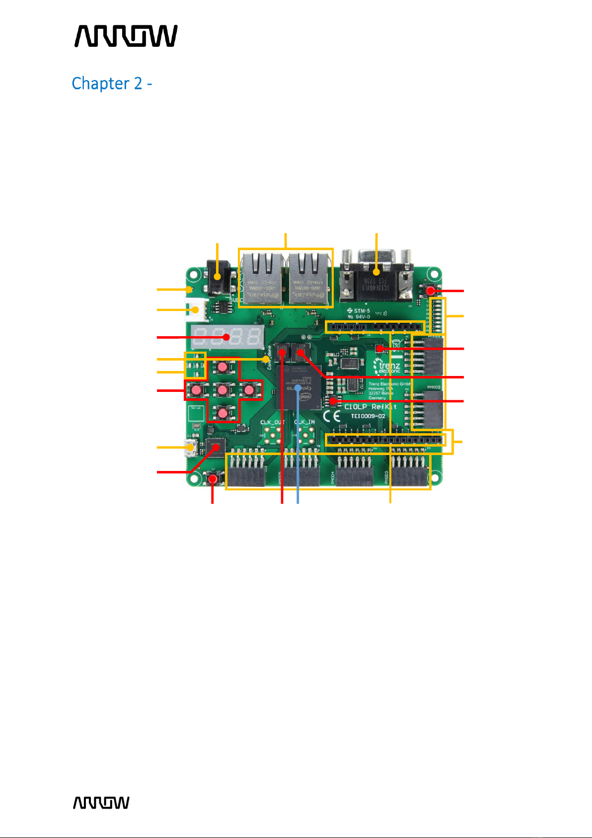
Introduction to the Cyclone 10 LP RefKit Board..................................................... 7
2.1 Layout and Components...................................................................................................7
2.2 Hardware variations .........................................................................................................9
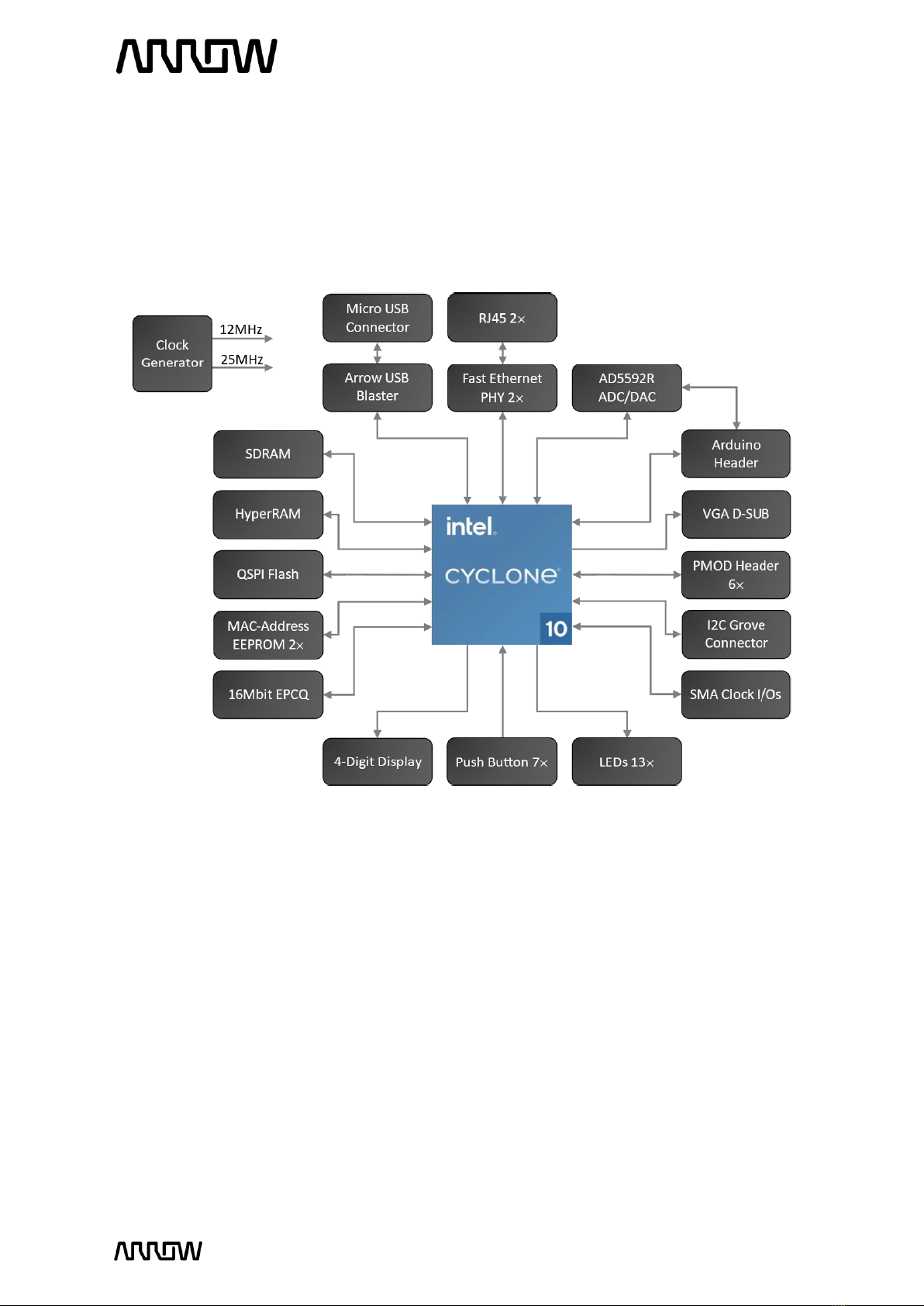
2.3 Block Diagram.................................................................................................................10
Connections and Peripherals of the Cyclone 10 LP RefKit Board .......................... 11
3.1 Board Status Elements....................................................................................................11
3.2 Clock Circuitry.................................................................................................................11
3.3 Peripherals Connected to the FPGA ...............................................................................12
3.3.1 Communication and Configuration.........................................................................12
3.3.2 Fast Ethernet...........................................................................................................14
3.3.3 Serial Configuration Flash Memory ........................................................................15
3.3.4 HyperRAM...............................................................................................................16
3.3.5 SDRAM Memory......................................................................................................17
3.3.6 QSPI Flash Memory.................................................................................................18
3.3.7 EEPROMs.................................................................................................................18
3.3.8 ADC/DAC .................................................................................................................19
3.3.9 I2C Grove Connector...............................................................................................20
3.3.10 Arduino Header.......................................................................................................21
3.3.11 PMOD Connectors...................................................................................................22
3.3.12 VGA..........................................................................................................................24
3.3.13 LEDs.........................................................................................................................25
3.3.14 Push Buttons ...........................................................................................................26
3.3.15 7-segment LED Display............................................................................................27
3.3.16 Power Tree..............................................................................................................28
Software and Driver Installation......................................................................... 30
4.1 Installing Quartus Prime Software..................................................................................30
4.2 Installing Arrow USB Programmer2................................................................................31
4.3 License ............................................................................................................................33

Cyclone 10 LP RefKit User Guide www.arrow.com
Page | 3 February 2022
New Project with Cyclone 10 LP RefKit ............................................................... 34
5.1 Creating a new Blinky Project with Cyclone 10 LP RefKit...............................................34
5.2 Building a Blinky Project with Cyclone 10 LP RefKit .......................................................39
5.2.1 Block Diagram .........................................................................................................39
5.2.2 Components of the Design......................................................................................39
5.2.3 Catalog IP ................................................................................................................40
5.2.4 Create and Configure PLL........................................................................................ 40
5.2.5 Create and Configure the Counter..........................................................................44
5.2.6 Create and Configure the Multiplexer....................................................................46
5.2.7 Adding the Components to the Schematic.............................................................48
5.2.8 Connecting the Components ..................................................................................50
5.2.9 Add inputs, outputs to the schematic.....................................................................53
5.2.10 Analysis and Synthesis ............................................................................................55
5.2.11 Adding Timing Constraints......................................................................................56
5.2.12 Pinning Assignments ...............................................................................................57
5.2.13 Compiling the Design ..............................................................................................60
5.2.14 Reading the Compilation Report.............................................................................61
Configuring the Cyclone 10 LP RefKit .................................................................. 63
6.1 Configure the FPGA in JTAG mode .................................................................................63
6.2 Serial configuration flash memory programming ..........................................................66
6.2.1 Programming File generation .................................................................................67
6.2.2 Device Programming...............................................................................................70
6.3 Testing the Design ..........................................................................................................71
Common Issues and Fixes................................................................................... 72
Appendix ........................................................................................................... 73
8.1 Revision History ..............................................................................................................73
8.2 Legal Disclaimer..............................................................................................................74

Cyclone 10 LP RefKit User Guide www.arrow.com
Page | 4 February 2022
Table of Figures
Figure 1 Cyclone 10 LP RefKit Board (top view)............................................................................7
Figure 2 Cyclone 10 LP RefKit Board (bottom view) .....................................................................8
Figure 3 - Cyclone 10 LP RefKit Block Diagram ..............................................................................10
Figure 4 Position of Indication LEDs............................................................................................11
Figure 5 Cyclone 10 LP RefKit Clock Tree....................................................................................12
Figure 6 JTAG Connections..........................................................................................................13
Figure 7 FTDI Connections ..........................................................................................................13
Figure 8 MAC-to-PHY connection ...............................................................................................14
Figure 9 Configuration Flash Connections ..................................................................................16
Figure 10 HyperRAM Connections..............................................................................................16
Figure 11 SDRAM Connections ...................................................................................................17
Figure 12 QSPI Flash Connections............................................................................................... 18
Figure 13 EEPROM Connections .................................................................................................19
Figure 14 ADC/DAC Connections ................................................................................................19
Figure 15 I2C Grove Connector...................................................................................................20
Figure 16 - Arduino Header Connections.......................................................................................21
Figure 17 PMOD Headers Connections.......................................................................................22
Figure 18 VGA Connections.........................................................................................................24
Figure 19 LED Connections..........................................................................................................25
Figure 20 Button Connections ....................................................................................................26
Figure 21 4-digit 7-segment Display Connections ......................................................................27
Figure 22 Quadruple Seven-............................28
Figure 23 Power Tree Connections.............................................................................................29

Cyclone 10 LP RefKit User Guide www.arrow.com
Page | 5 February 2022
Cyclone 10 LP RefKit Development Board
1.1 About Arrow Cyclone 10 LP RefKit Board
The Cyclone 10 LP Reference Kit is a customizable development board that targets all kinds of
applications with a wide range of interfaces. The board is based on Cyclone 10 LP FPGA, which is
optimized for low-cost and low-power designs, making them ideal for high-volume and cost-
sensitive applications. High-density sea of programmable gates and onboard resources allow
implementation of Nios II 32-bit microcontroller IP, which provides the ideal solution for I/O
expansion, chip-to-chip interfacing, industrial, automotive, and consumer applications.
The C10LP RefKit is equipped with an Arrow USB Programmer2, 2 ports 10/100Mbps Ethernet,
SDRAM, HyperRAM, flash memory, VGA, 8-channel ADC/DAC, PMODs, and ARDUINO connectors
making it a fully featured plug and play solution without any additional costs.
The C10LP RefKit board contains all the tools needed to use the board in conjunction with a
computer that runs a 64-bit Linux / Microsoft Windows 10 operating system or later.
1.2 Useful Links
A set of useful links that can be used to get relevant information about the Cyclone 10 LP RefKit
or the Cyclone 10 LP FPGA.
•Cyclone 10 LP RefKit at Arrow Shop
•Cyclone 10 LP RefKit at Trenz Electronic Shop
•Intel Cyclone 10 LP Webpage
•Cyclone 10 LP RefKit Wiki Page

Cyclone 10 LP RefKit User Guide www.arrow.com
Page | 6 February 2022
1.3 Getting Help
Here are the addresses where you can get help if you encounter any problems:
•Arrow Electronics
In Person
Arrow EMEA
+ 49 (0) 6102 5030 0
Online
https://arrow.com
•Trenz Electronic GmbH
https://www.trenz-electronic.de/en/

Cyclone 10 LP RefKit User Guide www.arrow.com
Page | 7 February 2022
Introduction to the Cyclone 10 LP RefKit Board
2.1 Layout and Components
Figure 1 and Figure 2 shows a top view and the bottom view of the board. It depicts the layout of
the board and indicates the location of the various connectors and key components.
Figure 1 –Cyclone 10 LP RefKit Board (top view)

Cyclone 10 LP RefKit User Guide www.arrow.com
Page | 8 February 2022
The following features are available on the Cyclone 10 LP RefKit board:
FPGA Device
•Intel Cyclone 10 LP 10CL055YU484C8G device.
Features of the FPGA on the C10LP RefKit:
Resources
Device
10CL055
Logic Elements (LE)
55,856
M9K Memory (Kb)
2,340
18 x 18 Multiplier
156
PLLs
4
I/O
321
Memory Devices
•64-256Mbit external SDRAM memory
1
•64Mbit external HyperRAM memory
•64-128Mbit external QSPI Flash memory1
•16Mbit EPCQ serial configuration flash memory
•22Kbit serial MAC-Address EEPROM memory
1
The different board variations are equipped with different memory devices
Figure 2 –Cyclone 10 LP RefKit Board (bottom view)

Cyclone 10 LP RefKit User Guide www.arrow.com
Page | 9 February 2022
Configuration and Debug
•On-board Arrow USB Programmer2 (micro-USB type B connector) JTAG mode
Interfaces
•210/100Mbps Ethernet PHYs with RJ45 connectors
•8-Channel, 12-bits configurable ADC/DAC
Connectors
•6PMOD Headers
•Arduino Uno R3 compatible Header
•VGA with 15-pin high density D-Sub connector
•I2C Grove connector
•Optional SMA connectors for preferred frequency
Buttons and Indicators
•4-Digit 7-Segment LED Display
•7Buttons
•13user LEDs
•2board status LEDs
Power
•Recommended external supply voltage range: +5.0 V (nominal)
•Recommended external supply current: 3 A
•Recommended I/O signal voltage range: 0 to +3.3 V
2.2 Hardware variations
Multiple board configurations are available with Cyclone 10 LP RefKit have different equipment.
This user guide covers REV02 hardware revision with 8C and 8CA featured boards.
These two boards are the same with the exception that different memory devices have been
mounted.
Ordering Code
SDRAM
SDRAM feature
QSPI Flash
QSPI Flash
feature
TEI0009-02-055-8C
IS42S16400J-7BL
64Mbit up to
143MHz
IS25LP064A-JBLE
64Mbit up to
133MHz
TEI0009-02-055-8CA
IS42S16160J-7BL
256Mbit up to
143MHz
IS25LP128F-JBLE
128Mbit up to
166MHz

Cyclone 10 LP RefKit User Guide www.arrow.com
Page | 10 February 2022
2.3 Block Diagram
Figure 3 represents the block diagram of the board. All the connections are established through
the Cyclone 10 LP FPGA device to provide maximum flexibility for users. Users can configure the
FPGA to implement any system design.
Figure 3 - Cyclone 10 LP RefKit Block Diagram

Cyclone 10 LP RefKit User Guide www.arrow.com
Page | 11 February 2022
Connections and Peripherals of the Cyclone 10 LP
RefKit Board
3.1 Board Status Elements
In addition to the 13 user LEDs that the FPGA can control, there are 2 additional board-specific
status LEDs that can indicate the status of the board.
Board Reference
LED Name
Description
D1
3.3V
On when 3.3V power is active
D10
CONF_DONE
On when configuration data was loaded to Cyclone 10 LP
device without error
3.2 Clock Circuitry
All the external clocks of the system can be seen in Figure 5. There are two default clocks which
are 12MHz and 25MHz. Both clock signals are connected and driving the FPGAs user logic and
other interfaces (Arrow USB Programmer2 and Ethernet). There are optional slots for other clocks
that you can either add another preferred clock source to the FPGA (CLK_IN_SMA) or generate an
FPGA-controlled clock (CLK_OUT_SMA). All clock signals are connected to the internal PLLs of the
FPGA.
For more information on clocks and PLLs of the Cyclone 10 LP, please refer to this document.
Figure 4 –Position of Indication LEDs

Cyclone 10 LP RefKit User Guide www.arrow.com
Page | 12 February 2022
Board Reference
FPGA Pin No.
Pin Func.
Description
I/O Std
CLK12M
PIN_G21
Input
12MHz clock input
3.3 V
CLK_25M
PIN_AA12
Input
25MHz clock input
3.3 V
CLK_IN_SMA
PIN_B11
Input
Optional clock input
3.3 V
CLK_OUT_SMA
PIN_E5
Output
Optional clock output
3.3 V
3.3 Peripherals Connected to the FPGA
3.3.1 Communication and Configuration
The C10LP RefKit board uses a single chip to perform configuration of the device and
communication over USB.
3.3.1.1 JTAG Chain Configuration
There are two types of configuration methods supported by C10LP RefKit:
1. JTAG Configuration: configuration using JTAG ports. JTAG configuration scheme allows you to
directly configure the device core through JTAG pins (TDI, TDO, TMS and TCK pins). The
Quartus Prime software automatically generates a .sof that can be downloaded to the Cyclone
10 LP with a download cable through the Quartus Prime Programmer.
2. Configuration from EPCQ-A flash: configuration using external flash. Before configuration,
you need to program the configuration data .jic into the configuration flash memory (EPCQ-
A) which provides non-volatile storage for the bit stream. The information is retained within
Figure 5 –Cyclone 10 LP RefKit Clock Tree

Cyclone 10 LP RefKit User Guide www.arrow.com
Page | 13 February 2022
EPCQ-A even if the C10LP RefKit is turned off. When the board is powered on, the
configuration data in the EPCQ-A is automatically loaded into the Cyclone 10 LP FPGA.
Board Reference
FPGA Pin No.
Pin Func.
Description
I/O Std
TCK
PIN_L2
Input
Test Interface Clock
3.3 V
TDO
PIN_L4
Output
Test Data Out
3.3 V
TDI
PIN_L5
Input
Test Data In
3.3 V
TMS
PIN_L1
Input
Test Mode Select
3.3 V
For detailed information about how to configure the Cyclone 10 LP, please refer to Chapter 6.
3.3.1.2 USB Communication
The FTDI chip converts signals from USB 2.0 to a variety of standard serial and parallel interfaces.
Channel A of FTDI chip is used in MPPSE mode for JTAG. Channel B is routed to FPGA and is usable
for other standard interfaces.
Figure 6 –JTAG Connections
Figure 7 –FTDI Connections

Cyclone 10 LP RefKit User Guide www.arrow.com
Page | 14 February 2022
Board Reference
FPGA Pin No.
Pin Func.
Description
I/O Std
BDBUS0
PIN_C20
Bidir
D[0] of bidirectional data bus
3.3 V
BDBUS1
PIN_B21
Bidir
D[1] of bidirectional data bus
3.3 V
BDBUS2
PIN_B22
Bidir
D[2] of bidirectional data bus
3.3 V
BDBUS3
PIN_C21
Bidir
D[3] of bidirectional data bus
3.3 V
BDBUS4
PIN_C22
Bidir
D[4] of bidirectional data bus
3.3 V
BDBUS5
PIN_D21
Bidir
D[5] of bidirectional data bus
3.3 V
BDBUS6
PIN_D22
Bidir
D[6] of bidirectional data bus
3.3 V
BDBUS7
PIN_E21
Bidir
D[7] of bidirectional data bus
3.3 V
BCBUS0
PIN_E22
Bidir
D[0] of bidirectional data bus
3.3 V
BCBUS1
PIN_F21
Bidir
D[1] of bidirectional data bus
3.3 V
BCBUS2
PIN_F22
Bidir
D[2] of bidirectional data bus
3.3 V
BCBUS3
PIN_H21
Bidir
D[3] of bidirectional data bus
3.3 V
BCBUS4
PIN_H22
Bidir
D[4] of bidirectional data bus
3.3 V
BCBUS5
PIN_J21
Bidir
D[5] of bidirectional data bus
3.3 V
BCBUS6
PIN_J21
Bidir
D[6] of bidirectional data bus
3.3 V
BCBUS7
PIN_J19
Bidir
D[7] of bidirectional data bus
3.3 V
3.3.2 Fast Ethernet
The board has two independent 10/100Mbps Ethernet ports with RJ-45 connectors. For the
physical layer, the Microchip KSZ8081 Ethernet PHY is used, which is suitable for general
applications.
The MAC-to-PHY interface is configured to a MII interface connections with MDIO interface as
management.
Board Reference
FPGA Pin No.
Pin Func.
Description
I/O Std
ETH1_MDIO
PIN_AA21
Bidir
Management Interface Data
3.3 V
ETH1_MDC
PIN_AA22
Output
Management Interface Clock
3.3 V
ETH1_COL
PIN_T19
Bidir
MII Collision Detect
3.3 V
ETH1_CRS
PIN_R20
Bidir
MII Carrier Sense
3.3 V
Figure 8 –MAC-to-PHY connection

Cyclone 10 LP RefKit User Guide www.arrow.com
Page | 15 February 2022
Board Reference
FPGA Pin No.
Pin Func.
Description
I/O Std
ETH1_RXDV
PIN_W21
Bidir
MII Receive Data Valid
3.3 V
ETH1_RST
PIN_R19
Output
Chip Reset
3.3 V
ETH1_INTRP
PIN_U22
Bidir
Interrupt
3.3 V
ETH1_RXC
PIN_V22
Bidir
MII Receive Clock
3.3 V
ETH1_RXER
PIN_V21
Bidir
MII Receive Error
3.3 V
ETH1_RXD0
PIN_W22
Bidir
MII Receive Data D[0]
3.3 V
ETH1_RXD1
PIN_W20
Bidir
MII Receive Data D[1]
3.3 V
ETH1_RXD2
PIN_Y21
Bidir
MII Receive Data D[2]
3.3 V
ETH1_RXD3
PIN_Y22
Bidir
MII Receive Data D[3]
3.3 V
ETH1_TXC
PIN_U21
Bidir
MII Transmit Clock
3.3 V
ETH1_TXEN
PIN_T18
Output
MII Transmit Enable
3.3 V
ETH1_TXD0
PIN_T17
Output
MII Transmit Data D[0]
3.3 V
ETH1_TXD1
PIN_U20
Output
MII Transmit Data D[1]
3.3 V
ETH1_TXD2
PIN_U19
Output
MII Transmit Data D[2]
3.3 V
ETH1_TXD3
PIN_T20
Output
MII Transmit Data D[3]
3.3 V
ETH2_MDIO
PIN_N20
Bidir
Management Interface Data
3.3 V
ETH2_MDC
PIN_N18
Output
Management Interface Clock
3.3 V
ETH2_COL
PIN_P21
Bidir
MII Collision Detect
3.3 V
ETH2_CRS
PIN_P22
Bidir
MII Carrier Sense
3.3 V
ETH2_RXDV
PIN_R18
Bidir
MII Receive Data Valid
3.3 V
ETH2_RST
PIN_M21
Output
Chip Reset
3.3 V
ETH2_INTRP
PIN_N17
Bidir
Interrupt
3.3 V
ETH2_RXC
PIN_R17
Bidir
MII Receive Clock
3.3 V
ETH2_RXER
PIN_P17
Bidir
MII Receive Error
3.3 V
ETH2_RXD0
PIN_M20
Bidir
MII Receive Data D[0]
3.3 V
ETH2_RXD1
PIN_M19
Bidir
MII Receive Data D[1]
3.3 V
ETH2_RXD2
PIN_M16
Bidir
MII Receive Data D[2]
3.3 V
ETH2_RXD3
PIN_N19
Bidir
MII Receive Data D[3]
3.3 V
ETH2_TXC
PIN_N16
Bidir
MII Transmit Clock
3.3 V
ETH2_TXEN
PIN_R22
Output
MII Transmit Enable
3.3 V
ETH2_TXD0
PIN_R21
Output
MII Transmit Data D[0]
3.3 V
ETH2_TXD1
PIN_N21
Output
MII Transmit Data D[1]
3.3 V
ETH2_TXD2
PIN_M22
Output
MII Transmit Data D[2]
3.3 V
ETH2_TXD3
PIN_N22
Output
MII Transmit Data D[3]
3.3 V
3.3.3 Serial Configuration Flash Memory
The C10LP RefKit board is integrated with a 16MBit of serial flash memory that can be used for
user data and programming non-volatile storage. The configuration bitstream is downloaded into
the serial configuration device which automatically loads the configuration data into the Cyclone
10 LP when the board is powered on. Device memory capacity not consumed storing
configuration data can be used as general-purpose non-volatile memory, which is perfect for
program and data storage. Several interfaces available with Nios II embedded processors allow
you to access the serial configuration device as a memory module connected to your embedded
system.

Cyclone 10 LP RefKit User Guide www.arrow.com
Page | 16 February 2022
Board Reference
FPGA Pin No.
Pin Func.
Description
I/O Std
AS_DATA
PIN_K1
Input
Data In
3.3 V
AS_DCLK
PIN_K2
Output
Clock
3.3 V
AS_NCS
PIN_E2
Output
Chip Select
3.3 V
AS_ASDO
PIN_D1
Output
Data Out
3.3 V
3.3.4 HyperRAM
A 64Mbit Pseudo Static Random Access Memory using a self-refresh DRAM array is integrated on
C10LP RefKit. The Cyclone 10 LP connects to this memory via a very low signal count interface,
called HyperBus.
Board Reference
FPGA Pin No.
Pin Func.
Description
I/O Std
HR_CLK
PIN_T16
Output
Single Ended Clock
3.3 V
HR_RW
PIN_U13
Bidir
Read Write Data Strobe
3.3 V
HR_CS
PIN_V13
Output
Chip Select
3.3 V
HR_RESET
PIN_U12
Output
Hardware Reset
3.3 V
HR_D0
PIN_T15
Bidir
Data [0]
3.3 V
HR_D1
PIN_W17
Bidir
Data [1]
3.3 V
HR_D2
PIN_U14
Bidir
Data [2]
3.3 V
HR_D3
PIN_R15
Bidir
Data [3]
3.3 V
HR_D4
PIN_R14
Bidir
Data [4]
3.3 V
HR_D5
PIN_V16
Bidir
Data [5]
3.3 V
HR_D6
PIN_U16
Bidir
Data [6]
3.3 V
HR_D7
PIN_U17
Bidir
Data [7]
3.3 V
Figure 9 –Configuration Flash Connections
Figure 10 –HyperRAM Connections

Cyclone 10 LP RefKit User Guide www.arrow.com
Page | 17 February 2022
3.3.5 SDRAM Memory
The C10LP RefKit board supports single-chip SDRAM with up to 256Mbit density
2
which can
operate up to 143 MHz clock frequency. Below are the connections and pinning of the SDRAM
used in the C10LP RefKit.
Board Reference
FPGA Pin No.
Pin Func.
Description
I/O Std
A0
PIN_V5
Output
SDRAM Address [0]
3.3 V
A1
PIN_Y3
Output
SDRAM Address [1]
3.3 V
A2
PIN_W6
Output
SDRAM Address [2]
3.3 V
A3
PIN_Y4
Output
SDRAM Address [3]
3.3 V
A4
PIN_AB5
Output
SDRAM Address [4]
3.3 V
A5
PIN_AB6
Output
SDRAM Address [5]
3.3 V
A6
PIN_AA6
Output
SDRAM Address [6]
3.3 V
A7
PIN_AA7
Output
SDRAM Address [7]
3.3 V
A8
PIN_AB8
Output
SDRAM Address [8]
3.3 V
A9
PIN_AA5
Output
SDRAM Address [9]
3.3 V
A10
PIN_V6
Output
SDRAM Address [10]
3.3 V
A11
PIN_AA8
Output
SDRAM Address [11]
3.3 V
A12
PIN_AB8
Output
SDRAM Address [12]
3.3 V
A13
PIN_AB9
Output
SDRAM Address [13]
3.3 V
BA0
PIN_Y6
Output
SDRAM Bank Address [0]
3.3 V
BA1
PIN_V7
Output
SDRAM Bank Address [1]
3.3 V
RAS
PIN_V8
Output
SDRAM Row Address Strobe
3.3 V
CAS
PIN_Y7
Output
SDRAM Column Address Strobe
3.3 V
WE
PIN_W8
Output
SDRAM Write Enable
3.3 V
CS
PIN_W7
Output
SDRAM Chip Select
3.3 V
CLK
PIN_AA3
Output
SDRAM Input Clock
3.3 V
CKE
PIN_AA4
Output
SDRAM Clock Enable
3.3 V
DQ0
PIN_AB16
Bidir
SDRAM Data [0]
3.3 V
DQ1
PIN_Y17
Bidir
SDRAM Data [1]
3.3 V
DQ2
PIN_AA16
Bidir
SDRAM Data [2]
3.3 V
DQ3
PIN_AA19
Bidir
SDRAM Data [3]
3.3 V
DQ4
PIN_AB18
Bidir
SDRAM Data [4]
3.3 V
DQ5
PIN_AA20
Bidir
SDRAM Data [5]
3.3 V
DQ6
PIN_AB19
Bidir
SDRAM Data [6]
3.3 V
DQ7
PIN_AB20
Bidir
SDRAM Data [7]
3.3 V
2
The size of the mounted SDRAM depends on the board variation. For detailed information, please refer to Chapter 2.2.
Figure 11 –SDRAM Connections

Cyclone 10 LP RefKit User Guide www.arrow.com
Page | 18 February 2022
Board Reference
FPGA Pin No.
Pin Func.
Description
I/O Std
DQ8
PIN_Y13
Bidir
SDRAM Data [8]
3.3 V
DQ9
PIN_Y15
Bidir
SDRAM Data [9]
3.3 V
DQ10
PIN_AA13
Bidir
SDRAM Data [10]
3.3 V
DQ11
PIN_AB15
Bidir
SDRAM Data [11]
3.3 V
DQ12
PIN_AB13
Bidir
SDRAM Data [12]
3.3 V
DQ13
PIN_AA15
Bidir
SDRAM Data [13]
3.3 V
DQ14
PIN_AA14
Bidir
SDRAM Data [14]
3.3 V
DQ15
PIN_AB14
Bidir
SDRAM Data [15]
3.3 V
DQM0
PIN_Y14
Output
SDRAM Lower Data Mask
3.3 V
DQM1
PIN_W13
Output
SDRAM Upper Data Mask
3.3 V
3.3.6 QSPI Flash Memory
There is a non-volatile, QSPI Flash memory with up to 128Mbit density
3
which can operate on up
to 166MHz on the board. It can be used to store larger size user data or software for Nios II
embedded processors.
Board Reference
FPGA Pin No.
Pin Func.
Description
I/O Std
F_CS
PIN_F15
Output
Chip Enable
3.3 V
F_CLK
PIN_F16
Output
Serial Data Clock
3.3 V
F_IO0
PIN_G16
Bidir
Serial Data [0]
3.3 V
F_IO1
PIN_D15
Bidir
Serial Data [1]
3.3 V
F_IO2
PIN_E16
Bidir
Serial Data [2]
3.3 V
F_IO3
PIN_E15
Bidir
Serial Data [3]
3.3 V
3.3.7 EEPROMs
The C10LP RefKit board has 2 pieces 2Kb serial EEPROMs that can be used for MAC address
configuration. The EEPROMs are pre-programmed with a globally unique EUI-48 node address.
3
The size of the mounted QSPI Flash depends on the board variation. For detailed information, please refer to Chapter 2.2.
Figure 12 –QSPI Flash Connections

Cyclone 10 LP RefKit User Guide www.arrow.com
Page | 19 February 2022
Board Reference
FPGA Pin No.
Pin Func.
Description
I/O Std
I2C_SDA
PIN_F17
Bidir
Serial Data Line
3.3 V
I2C_SCL
PIN_D20
Output
Serial Clock Line
3.3 V
3.3.8 ADC/DAC
The C10LP RefKit is equipped with an 8-channel, 12-bit, configurable analog-to-digital, digital-to-
analog converter. There are 2 dedicated through-hole connection points on the board for 2 analog
channels, while the remaining 6 channels are directly connected to the J4 header of the Arduino
interface.
Board Reference
FPGA Pin No.
Pin Func.
Description
I/O Std
ADDA_RSTN
PIN_V4
Output
Reset
3.3 V
ADDA_SYNC
PIN_R5
Output
Synchronization
3.3 V
MCLK
PIN_T5
Output
Serial Clock Input
3.3 V
MOSI
PIN_T4
Output
Master Output Slave Input
3.3 V
MISO
PIN_R6
Input
Master Input Slave Output
3.3 V
Figure 13 –EEPROM Connections
Figure 14 –ADC/DAC Connections

Cyclone 10 LP RefKit User Guide www.arrow.com
Page | 20 February 2022
Board Reference
Connector
Description
AREF
J1 / 8
External Reference Voltage
AIN0
J4 / 1
Analog I/O Channel 0
AIN1
J4 / 2
Analog I/O Channel 1
AIN2
J4 / 3
Analog I/O Channel 2
AIN3
J4 / 4
Analog I/O Channel 3
AIN4
J4 / 5
Analog I/O Channel 4
AIN5
J4 / 6
Analog I/O Channel 5
AIN6
TP1
Analog I/O Channel 6
AIN7
TP2
Analog I/O Channel 7
3.3.9 I2C Grove Connector
There is a Grove connector which allows external, I2C compatible devices to be connected to the
C10LP RefKit board.
Board
Reference
FPGA Pin
No.
Grove Pin
Pin
Func.
Description
I/O Std
I2C_SCL
PIN_D20
1
Output
Serial Clock Line
3.3 V
I2C_SDA
PIN_F17
2
Bidir
Serial Data Line
3.3 V
3.3V
-
3
PWR
3.3V power to the connector
-
GND
-
4
PWR
Ground output to the connector
-
Note: The FPGA is also directly connected to the J4 connector. If AIN5..0 are used as analog
input/output, make sure that the belonging FPGA I/Os are unused and configured as
input tri-stated!
Note: Do not drive a voltage greater than 3.3V to the analog I/Os. Voltages greater than
3.3V can cause irreversible damage to the FPGA!
Figure 15 –I2C Grove Connector
Note: The EEPROMs are also connected to this I2C bus, 0x50h and 0x51h addresses are
reserved for these EEPROMs.
Table of contents
Other Arrow Desktop manuals