BBK AB217 User manual

ENGLISH
AB217
SERVICE MANUAL

1 Circuit Makeup.................................................................................................
Block Diagram...................................................................................................
2 Power SupplyCircuit........................................................................................
3 Input Circuit.....................................................................................................
4 Volume, Tone and BalanceAdjusting Circuits...................................................
5 Microphone Circuits.........................................................................................
5.1 Working Principle of the Front Processing Section..............................................
5.2 Working Principle of the Echo Processing Section...............................................
6 Front PanelControl and DisplayCircuits..........................................................
6.1 Input ControlSection........................................................................................
6.2 Channel andMIC Delay Section.........................................................................
6.2.1 Channel SelectionSection.............................................................................
6.2.2 The MIC Delay Selection Section....................................................................
6.3 The Spectrum Analysis Section.........................................................................
7 PowerAmplification and ProtectionCircuits....................................................
7.1 PowerAmplification Section..............................................................................
7.2 Protection Circuit.............................................................................................
7.2.1 Delay Switch-onProtection Circuit..................................................................
7.2.2 Midpoint Over-voltageCircuit.........................................................................
7.2.3 Short CircuitOver-current Protection..............................................................
7.3 Multi-channel ControlCircuit............................................................................
8 Detailed CircuitExplanations...........................................................................
8.1 The Power Amplifying Board.............................................................................
8.1.1 Main PartsList of The Matin Power Amplifying Board........................................
8.1.2 Schematic DiagramOf The Main Amplifying Board...........................................
8.2 Front Panel'sControl Board..............................................................................
8.2.1 Main PartsList of The Front Panel's Control Board...........................................
8.2.2 Schematic Diagramof The Front Panel's Control Board....................................
8.3 Potentiometer Board........................................................................................
8.3.1 Main PartsList of The Potentiometer Board.....................................................
8.3.2 Schematic Diagramof The Potentiometer........................................................
9 The ExplanationFor Key Components.............................................................
CONTENTS
1
2
3
4
5
6
6
6
7
7
9
10
10
11
12
13
13
14
14
15
15
16
16
16
18
19
19
22
24
24
25
26
- 27 -
NAME OF PINS I/O DESCRIPTION NUMBER OF PINS
VDD PDIGITAL POWER INPUT 1
XI N IOSCILLATOR INPUT 2
XOUT OOSCILLATOR OUTPUT 3
D1 / REQ I
SIMPLE MODE: D1 DATA INPUT
MICRO CONTROL MODE: DEMAND
SIGNAL 4
D2 / SCK I
SIMPLE MODE: D2 DATA INPUT
MICRO CONTROL MODE: TIME
PULSE INPUT 5
D3 / DATA I
SIMPLE MODE: D3 DATA INPUT
MICRO CONTROL MODE: DATA INPUT 6
D4/IDSW I
SIMPLE MODE: D4 DATA INPUT
MICRO CONTROL MODE:
IDENTIFYING CODE INPUT 7
TEST IEXCLUSIVELY FOR THE TEST. BE
GROUNDED WHEN IN DAILY USE. 8
EASY/ U- COM I
HIGH POTENTIAL£º
SIMPLE MODE
LOW POTENTIAL: MICRO CONTROL
MODE 9
SLEEP I
HIGH POTENTIAL£º
SLEEP MODE
LOW POTENTIAL: NORMAL MODE 10
D- GND GDIGITAL 11
A- GND GANALOG 12
LPF2 OUT OLOW PASS FILTER 2 OUTPUT 13
LPF2 I N ILOW PASS FILTER 2 INPUT 14
OP2 OUT OINTEGRATOR 2 OUTPUT 15
OP2 IN IINTEGRATOR 2 INPUT 16
CC2 \CURRENT CONTROL 2 17
CC1 \CURRENT CONTROL 1 18
REF \ANALOG REFERENCE VOLTAGE
£ ¨=1/ 2Vcc£ © 19
OP1 I N IIN INTEGRATOR 1 INPUT 20
OP1 OUT IINTEGRATOR 1 OUTPUT 21
LPF1 OUT \LOW PASS FILTER 1 OUTPUT 22
LPF1 I N OLOW PASS FILTER 1 INPUT 23
Vcc PANALOG POWER INPUT 24
FUNCTIONS OF THE PINS

1.3 Volume and Tone Adjusting Circuits
Adjusts master volume and treble and bass tone of input signals.
1.4 Power Amplification and Protection Circuits
Amplifies input signals' power to drive speakers to produce sound; Protects circuits of speakers
and power amplifier automatically in abnormal conditions.
1.5 Microphone Circuit
Adjusts volume and tone of signals from the microphone and superimpose them on left and right
channels after echo processing.
1.6 Main Board Control and Display Circuits
Receives control commands and send control signals to achieve control function. Drives the VFD
screen to show the current working mode.
1 Circuit Makeup
This unit's circuit can be divided into six parts.
1.1 Source Circuit
Supplies power to each circuit unit.
1.2 Input Circuit
Selects one of four lines of input analog signals and sends it to the rear circuit.
- 1 - - 26 -
9 The Explanation For Key Components
IC Sc6931P
VDD
XIN
XOUT
D1/REQ
D2/SCK
D3/DATA
D4/IDSW
TEST
SLEEP
D-GND
A-GND LPF2OUT
LPF2IN
OP2OUT
OP2IN
CC2
LPF1IN
LPF1OUT
OP1OUT
OP1IN
REF
CC1
VCC
EASY/U-COM
1
2
3
4
5
6
7
8
9
10
11
12 13
14
15
16
17
18
19
20
21
22
23
24

N401
CD4052
Input
Selection
REC
DVD
VCD
CD
TAPE
RP901
Master
Volume
Adjustment
N901
Buffer
Amplification
RPH01
Balance
N903
Echo
Amplification
Left Channel's
Power
Amplification
Right Channel's
Power
Amplification
Protection
Circuit
RP902
RP903
N902
Tone
Adjustment
Push
Button
Matrix
Spectrum
Level
Comparison
Front
Panel's
Function
Control
VFD
Screen
N601A
N601B
Simultaneous
Two Lines
Amplification
N905
SC6931
Echo
Processing
MIC Muffling
BLOCK DIAGRAM (Figure 1)
N906A
Level Sampling
Amplification
2 CH
and
5 CH
Switch
RP601
RP602
Volume
Adjustment
RP603
RP604
N906B
Tone
Adjustment
V601
Echo
Signal
Amplification
Power
Supply
Circuit
Speakers
L
R
L
R
C
SR
SL
MIC1
MIC2
OK-SW
- 2 -- 25 -
8.3.2 Schematic Diagram ofThe Potentiometer
RPH01A
B50K
RPH01B
B50K
1
2
3
4
5
XP7
5PIN
L2
L3
R2
R3
GND
R917
2.2K
R918
2.2k

- 3 - - 24 -
2. Volume adjustment, sound field processing and EQ adjustment
circuits.
All channel signalsare sent toN402 inside whichthe independent volumeadjustment,
EQ adjustment andall sound fieldmodes process areperformed.
The sound fieldprocessing and EQadjusting circuit ismainly processing theL&R
channel signals.According to theschematic diagram, theL&R channel signalsare
added simultaneously tothe pins 15,17, 13 and16 of N402.When the unitmode is in
the Hi-Fi mode,the internal circuitof the pins17&16 is connectedand the otherinput
signals are cutoff.At this time,only the L&Rchannel volume canbe adjusted andonly
the pins 31&32send out signals.Therefore, theunit is inthe 2CH outputmode. The
unit mode isnot in theHi-Fi mode, otherinput signals areconnected but thepins
17&16 signals arecutoff.At this time,all channel volumescan be adjusted
independently and thesound field processingor EQ adjustingof the L&Rchannels
can be performed.Finally,all channel signalspass out fromthe pins 31,32, 33, 34,
35&36. TheSW channel signalfrom the pin36 reaches theamplified speakers tobe
amplified through theSW output terminals.Other channel signalsreach to thepower
st
amplifying circuit tobe amplified.The L&R channelsignals will gothrough 1 grade
LPF and MIXamplification (Karaoke signalsare overlapped intoL& R channels).
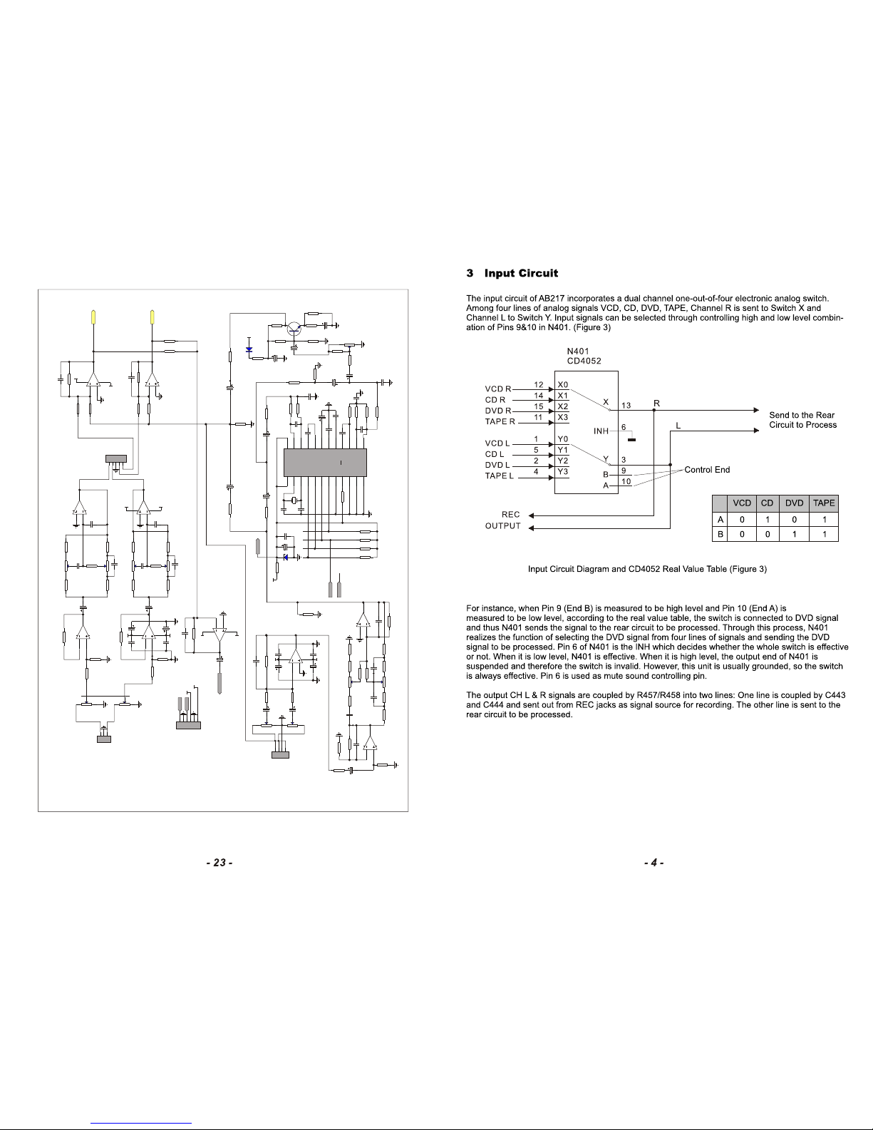
3. Input signals detect, search and frequency spectrum sampling cir
cuits
3.1 Input signalsdetect and searchcircuit: Thesix channel signallines of theinput IC
N402 are connectedwith 100K samplingresistors R533, R534,R657, R676 andR678
respectively.The signalsare mixed bythese resistors andadded to theopposite-phase
input terminal tobe amplified. VD431and C481 connectedto N403B's outputend
constitute half-wave rectifyingfilter circuit.Then the signalsreach the voltagecomparer
composed of N403A.The outputend of N403A(SEARCH)is connected tothe pin 28of
CPU. Thiscontrol signal isthe search anddetect signal: whenit is lowlevel, it entersthe
search mode; whenit is highlevel, it stopssearching. Its worksas follows:
3.1.1 When thisunit is gettingstarted, theA&B control signalsfrom the pins38&39 in
the domination ofthe CPU's interprogram are addedto the inputselect circuit to
search circularly once.When there areno signals inthese four inputconnectors, the
VCD mode stopsautomatically.When there aresignals in oneof the fourconnectors,
AC signals willappear in allchannels of theinput N402.These ACsignals are
amplified by N403Band rectified andfiltered by VD434and C481 tobecome DC
signals. Atthis time, theopposite-phase voltage ofN403A is0.01V.When this DC
voltage surpasses 0.01V, the outputend of N403Bsends out ahigh level (SEARCH)
close to positivepower supply voltage(A+6V) which reachesthe pin 28of CPU. CPU
keeps searching inthe connector inwhich there areinput signals andthe unit willplay
normally.
1.2.2 When pressthe SEARCH onthe front panel,CPU sends outA&B control
signals again tostart searching. Meanwhile,the pin 27(EX) sends outa high level
which makes V446inductive. Theemitter of V446sends out ahigh level whichpasses
through R498 whichmakes the opposite-phasevoltage of N403Ato be 0.4V. Thatis
to say, if youwant to stopsearching of CPU,the gained voltageafter the inputsignals
are rectified andfiltered must exceed0.4V.This voltageis higher than0.01V when
this unit isgetting started inorder to avoidthat the CPUreceives signals mistakenly
and stops searchingdue to thelarge external interferencesignals. If theinput signals'
amplitude is nothigh enough, CPUwill continue searching.When the amplitudeis
high enough, N403Asends out highlevel to thepin 28 tostop searching.The pin 27
(EX) will becomelow level againand the opposite-phasevoltage of N403Awill also
returns back to0.01V.The wholesearching process isfinished.

RP901A
B50K
RP901B
B50K
5
6
7
N902B
4558
5
6
7
N901B
4558
3
2
1
84
N902A
4558
R906
10k
R901
10k
R902
10K
R905
10k
C901
47u/16V
C902 47u/16V
-12V
+12V
R911
10K
R909
22K
R914
22K
R912
10K
R910
10K
R907
10K
R908
10K
RP902B
B50K
RP903B
B50K
RP903A
B50K
RP902A
B50K
C905
152
C908
152
R913
10K
R915
10K
R916
10K
C903
1u/16V
C904
1u/16V
C906
683
C909
683
C907
101
C910
101
+12V
-12V
R925
100k
R926
100k
1
2
3
4
5
6
XP5
6PIN
R927
470k
ToAMPBoard
TREBLE
BASS
BASS
TREBLE
ToAMPBoard
1
2
3
XP4
3PIN
L1
R1
GND
3
2
1
84
N601A
4558
R602
1k
R601
1k
R603
47k
RP602
C50K
-12V
+12V
MIC1
MIC2
FromMIBoard
1
2
3
4
XP6
4PIN
RP601
C50K
R4
L4
+12V
GND
-12V
GND
K-MUTE
R635
150/0.5W
+12V
-12V
R622
10k
C632
4.7u/16V
C621
224
C625
562
C622
224
C619
104
C617
561
R628
15k
RP605
B50k
C616
4.7u/16V
C618
562
R627
10k
R621
3.3k
C620
47u/16V
R624
12K
R623
15k
C615
4.7u/16V
C626
561
C624
104
VDD
1
XIN
2
XOUT
3
D1/REQ
4
D2/SCK
5
D3/DATA
6
D4/IDSW
7
TEST
8
EASY/CM
9
SLEEP
10
DGND
11
AGND
12
VCC 24
L1 IN 23
L1 OUT 22
O1 OUT 21
O1 IN 20
REF 19
CC1 18
CC2 17
O2 IN 16
O2 OUT 15
L2 IN 14
L2 OUT 13
N905 SC6931
G601
2M
C628
30p
C629
30p
R626
15k
R625
10k
R634
10k
R631
10k
R632
10k
R630
10k
R633
10k
C627
103
C630
47u/16V
R636
10k
R618
47k
5
6
7
N601B
NJM4558
R921
27K
R922
10K
R919
10k
3
2
1
84
N903A
4558
5
6
7
N903B
4558
R924
27k
R920
27k
R923
27K
C912
101
+12V
C911
101
3
2
1
84
N906A
4558
C913
101
C914
4u7/16V
R904
100k
+12V
-12V
C603
101
C614
4.7u/16V
R607
1.5k
R606
3.9k
+12V
VD601
5.1V
R903
100K
+5V
150mS
180mS
LEVEL
R4
L4
L4
R4
-12V
1
2
3
4
5
XP7
5PIN
TobanlanceBoard
R2
L2
L3
R3
GND
3
2
1
84
N901A
4558
C604
47uF/16V
C606
47uF/16V
C607
104
C605
104
C953
104
C952
104
C631
103
C635
470u/16V
R605
100K
R604
10k
C608
10u/16V 5
6
7
N906B
NJM4558
R6128.2k
RP604
B20k
RP603
B20k
C610
123
R614
10k
R615
20k
C611
471
BASS
TREBLE
C612
104
R608
12k
R616
10k
R613
10k R617
470k
C613
47p
R609
20k
R611
4.7k
R610
8.2k
C609
47p
R620
10k
R619
15k
C623
4.7u/16V
R629
2.2k
R644
47k
C633
4.7u/16V
V601
9014
R639
5.6k R640
4.7k
R641
8.2k
C634
10u/16V
R637
220k
R638
100k
C636
4.7u/16V
R643
10k
R642
1k
VD602
1N4148
+12V
C601
10u/16V
C602
10u/16V
R946
4.7k


47 CD CD11C 50V1U±20%4×7 1.5 C903,C904,C941
48 CD CD11C 50V10U±20%5×7 2 C601,C602,C608
49 CD CD11C 16V47U±20%5×7 2 C620,C630
50 CD CD11 35V220U±20£¥
10×15
5C956,C947
51 DIODE 1N4004 VD912,VD914
52 DIODE 1N4148 VD903~VD911,VD916,VD602
53
VOLTAGE
REGULATOR
DIODE
5.1V 1/2W VD601,VD915
54
VOLTAGE
REGULATOR
DIODE
24V 1/2W VD913
55 TRIODE 2N5551 V901
56 TRIODE 9014C V601
57 IC LM324N DIP N907,N910,N911,N912
58 IC NJM4558D DIP N901~N903,N906,N601
IC 4558C DIP N901~N903,N906,N601
59 IC CD4013BCN DIP N908
60 IC SC6931P DIP N905
61 CRYSTAL
OSCILLATOR 2.00MHz 49-U G601
62 VFD YW-3707A VFD901
63
LIGHT
TOUCH
RESTORE
SWITCH
VERTICAL 6×6×1 S901~S906
64 PCB 9217-4
65 CONNECTION
CORDS ¦µ
0.6 SHAPED 7.5mm
W1~W4,W7~W9,W11~W13,W16,W19~W22,W29,
W31~W34,W37,W38,W43,W46,W49,W52,W54,
W56~W58,W62,W65~W69,W74,W75,W81,W82,W83,
W90~W93,W99,W102,W103,W114,W116,W117
66 CONNECTION
CORDS ¦µ
0.6 SHAPED 10mm
W5,W17,W18,W23~W28,W35,W36,W39,W40,W42,
W47,W48,W59,W64,W70~W72,W76,W84~W86,W94,
W95,W98,W100,W101,W104,W109~W112,W115
67 CONNECTION
CORDS ¦µ
0.6 SHAPED 12.5mm W10,W14,W15,W30,W44,W51,W61,W77,W78,W88,
W89,W107,W108,R1013
68 CONNECTION
CORDS ¦µ
0.6 SHAPED 15mm W6,W41,W45,W50,W53,W55,W60,W63,W73,W79,
W80,W87,W96,W97,W113
69 CONNECTION
CORDS ¦µ
0.6 SHAPED 20mm W105,W106
CORDS 24# 50mm BLACK
70 RAFT CORDS 3P360 2.5 2 PLUG WITH L
NEEDLE XP3
71 RAFT CORDS 5P60 2.5 2 PLUG WITH L
NEEDLE XP7
72 RAFT CORDS 3P80 2.5 2 PLUG WITH L
NEEDLE XP2
73 RAFT CORDS 3P360 2.5 2 PLUG WITH L
NEEDLE , 2P SHIELDED XP4
74 RAFT CORDS 4P60 2.5 2 PLUG WITH L
NEEDLE, 3P SHIELDED XP6
75 RAFT CORDS 6P360 2.5 2 PLUG WITH L
NEEDLE, 2P SHIELDED XP5
76 SOFT SPONGE
SPACER
10×10×5 DOUBLE
FACED, HARD VFD/PCB


1. A+25Vpasses C941 andR983 and addsan instantaneous high level at the Pin 12 of
N907D when thisunit gets started. According to the above characteristics, the Pin 14 sends
out a voltagewhich is comparatively closer to the voltage of the power supply B+23V. This
voltage measures about+17V and is fed back to the Pin 12 through R960. Then this voltage
is divided intoabout +8.5V by the resistor R959. That is to say, the inphasevoltage of the
calculating amplifier N907Dkeeps at about +8.5V. At thesame time, +8.5V is divided by
VD903, R971 andR972 and the voltage of the Pin13 of N907D measures about +7.5V. That
is to say, the inphaseopposition of N907D keeps at about +7.5V. At this moment, the inphase
voltage (ca +8.5V)of the calculating amplifier N907D is higher than the inphase opposition
voltage (ca +7.5V).The output Pin 14 also keeps at about +17V. Therefore, the above status
retains. The Pin 14's high level of +17V passes R961 and reaches the display screen and
lightens the VCDindicator. The 0 level is obtained at the controllers A&B of theelectronic
switch in theinput circuit. According to the real value table, the electronic switch elects the
VCD input mode.C941 is the open restoration capacitor because of which the input mode
is switched tothe default VCD. The inphase opposition voltage of another three calculating
amplifiers is +7.5V(Their inphase opposition ports are connected together), but the positive
voltage doesn't existin the inphase ports. According to the voltage comparing characteristics,
there is notthe high level output in the inphase opposition ports. The other three input modes
are shut off.
2. When weselect other input modes, for instance, selecting DVD mode, we press the switch
S903. The voltage of B+23V passes R984, S903 and R965 and is divided into about +18V
voltage which issent to the inphase port of N907A. At the same time, the +18V voltage is
divided by VD905,R971 and R972 and there is about +17V level input at the inphase
opposition port ofN907A. The high level from N907A is fed back by R966. When loosening
S903, N907's workingvoltages (The working principle is the same as that in the above-
mentioned VCD mode.)are as follows: +8.5V at inphase port, +7.5V at inphase opposition
port, +17V atoutput port. As mentioned before, the inphase opposition port's voltage is +17V
when the switchis turned on. This voltage also reaches the calculating amplifier N907in the
VCD mode. Becausethe inphase port of N907D remains +8.5V and the inphase opposition
port increases to+17V, the original outputmode is breached and the high level cannot be
sent out. Therefore, the VCD mode is shut off. Atthis moment, the high level of +17V of
N907A's output isdivided into two lines: One line is sent to the display screen by R967 to
lighten the DVDindicator. Another line is divided by VD908, R974 and R975 and sent to the
Port B ofthe electronic switch in the input circuit. Now, the Port A of N401 is 0level and the
Port B ofN401 is 1 level. According to the real value table, the electronic switch selects the
DVD mode, andthe whole process is finished. When selecting other modes and pressing
other switches, thecaused motions are the same as above ones.
- 8 -- 19 -
8.2 Front Panel's Control Board
8.2.1 Main Parts List of The Front Panel's Control Board
NO. DESCRIPTION SPECIFICATIONS / PART
NUMBER LOCATION SPECIFICATIONS
1CARBON FILM
RESISTOR
1/4W470¦¸
±5% SHAPED
10 R979,R990,R994,R997,R1000,R1003,R1006,R1009,R1010
2CARBON FILM
RESISTOR 1/4W1K±5% SHAPED 10 R601,R602,R961,R964,R967,R970,R982,R988,R1016,
R1012,R1007,R985,R1014,R642
3CARBON FILM
RESISTOR 1/4W1.5K±5% SHAPED 10 R607
4CARBON FILM
RESISTOR 1/4W2.2K±5% SHAPED 10 R629,R1004,R977,R978
5CARBON FILM
RESISTOR 1/4W3.3K±5% SHAPED 10 R991,R621
6CARBON FILM
RESISTOR 1/4W3.9K±5% SHAPED 10 R606
7CARBON FILM
RESISTOR 1/4W4.7K±5% SHAPED 10 R1001,R611,R946,R640
8CARBON FILM
RESISTOR 1/4W5.6K±5% SHAPED 10 R639
9CARBON FILM
RESISTOR 1/4W10K±5% SHAPED 10
R901,R902,R905~R908,R910~R913,R915,R916,R919,
R922,R957,R971,R989,R995,R981,R987,R1015,R604,
R613,R614,R616,R620,R622,R625,R627,R630~R634,
R636,R643
10 CARBON FILM
RESISTOR 1/4W12K±5% SHAPED 10 R608,R624
11 CARBON FILM
RESISTOR 1/4W15K±5% SHAPED 10 R623,R626,R628,R619
12 CARBON FILM
RESISTOR 1/4W20K±5% SHAPED 10 R975,R976,R609,R615
13 CARBON FILM
RESISTOR 1/4W22K±5% SHAPED 10 R993,R996,R999,R1002,R984,R1008,R1005,R909,R914
14 CARBON FILM
RESISTOR 1/4W47K±5% SHAPED 10 R973,R974,R980,R983,R959,R960,R603,R618,R644
15 CARBON FILM
RESISTOR
1/4W100K±5% SHAPED
10
R903,R904,R925,R926,R962,R965,R968,R972,R963,
R966,R969,R992,R958,R605,R638
16 CARBON FILM
RESISTOR
1/4W220K±5% SHAPED
10 R1011,R637
17 CARBON FILM
RESISTOR
1/4W470K±5% SHAPED
10 R927,R617
18 CARBON FILM
RESISTOR 1/4W30K±5% SHAPED 10 R920,R921,R923,R924
19 CARBON FILM
RESISTOR 1/4W8.2K±5% SHAPED 10 R998,R610,R612,R641
20 CARBON FILM
RESISTOR 1/2W2K±5£¥
SHAPED 12.5 R986
21 CARBON FILM
RESISTOR
1/2W150¦¸
±5% SHAPED
12.5 R635
22
ROTATING
POTENTIO-
METER
A145GOED-H1B503-007 RP901
ROTATING
POTENTIO-
METER
A145GOED-H1B503-007-
01 RP901
ROTATING
POTENTIO-
METER
A145GOED-H1B503-007-
02 RP901
23
ROTATING
POTENTIO-
METER
A145GOED-H1B503-008 RP902,RP903

6.2 Channel and MIC Delay Selection
The delay circuitis made upof the Dtriggers N908A, N908Band voltage comparersN910B,
N910C, N911A. The inching switch S905 is the channel selection button in the front panel.
S906 is theMIC delay selectionbutton.
D, R andS are thecontrollers. It's lowlevel when Ris grounded. CLKis the triggeringport
whose output modeoverturns when ahigh level comes.When A+25Vpasses through R980
and R991, theinphase opposition voltageof those fourvoltage comparers isdivided into
about +1.6V. The working modes are as follows. (Figure 8)
Input Port Output Port
The Real Value Table of the D Trigger
CLK
/
/
D
/
0
1
0
R
0
0
0
0
S
1
0
0
0
Q
1
1
0
1
O
0
0
1
0
Figure 8
1
2
3
A
B
Ex
XP3
VD916
R990
V-5CH
~
- 9 - - 18 -
8.1.2 Schematic Diagram Of The Main Power Amplifying Board
V424
C9014
V405
2N5551
V423
C9014
V407
2N5551
V409
D718
V426
C9014
V421
C9014
V427
C9014
V404
2N5401
V410
B688
V408
2N5401
R401
220
R452
220/3W
R451
220/3W
R438
2.7k
R408
680
R406
1k
R416
0.25/3W
R415
0.25/3W
R414
220
R453
3k3
R403
4k7
R402
22k
C401
10u/16V
C405
33
C402
271
R417
220
R418
22k
C406
10u/16V
C407
271
R433
3.9k
R435
2.7k
R439
10/2W
R434
3.9k
R447
1M
C413
104
12
34
56Y401
DC 24V
VD405
1N4148
VD406
1N4148
VD407
1N4004
R461
47k
R444
10k
R445
10k
R450
47/3W
R462
47k
C416
220u/25V
C415
220u/25V
VD408
1N4004
C418
100u/35V
C422
6800u/35V
C425
47u/16V
C423
470u/25V
C426
47u/16V
C424
470u/25V
C421
6800u/35V
C431
102
CD R
VCD L
DVD R
VCD R
DVD L
TAPER
TAPEL
CD L
C
L
SL
SR
R
FL402
T6.3A/250V~
FL401
T6.3A/250V~
X0
12
X1
14
X2
15
X3
11
Y0
1
Y1
5
Y2
2
Y3
4
INH 6
A10
B9
VEE
7
X13
Y3
168
N401
CD4052
C430
47u/16V
R456
1k
VD416
6.8V
VD417
6.8V
R455
1k
C429
47u/16V
-12V
+12V
+33V
-33V
R413
22k
+33V
-33V
V425
C9015
C411
1u/16V
L 1
R 1
A
B
Ex
C403
47u/25V
C417
10u/50V
To VFD Board
To VFD Board
FromTrans
1
2
3
XS3
3PIN
C420
224
C419
224
R446
10k
1
2
3
XS4
3PIN
VD402
1N4148
VD401
1N4148
R409
150
V422
C9014
R436
3.9k
R440
10/2W
R437
3.9k
C414
104
+33V
-33V
C412
1u/16V
V429
2N5401
V428
2N5551
VD415
12V
VD414
12V
R454
3k3
C427
100u/16V
C428
100u/16V
+12V
-12V
R457
1k
R458
1k
C432
102
C435
10u/50V
C436
10u/50V
C437
10u/50V
C438
10u/50V
V401
2N5551 V402
2N5551
R405
10k
V403
2N5551
R407
22k
R404
4k7
V406
C9014
R411
3k
R412
1.2k
C404
33
R410
150
V415
2N5551
V417
2N5551 V419
D718
V414
2N5401
V420
B688
V418
2N5401
R424
680
R422
1k
R432
0.25/3W
R431
0.25/3W
R430
220
R419
4k7
C410
33
R429
22k
C408
47u/25V
VD404
1N4148
VD403
1N4148
R425
150
V412
2N5551
R421
10k
V413
2N5551
R423
22k
R420
4k7
V416
C9014
R427
3k
R428
1.2k
C409
33
R426
150
V411
2N5551
R443
1k
VD410
1N5404
VD411
1N5404
VD412
1N5404
VD413
1N5404
V430
2N5551
V431
2N5401
V432
2N5551
V433
2N5401
C433
10p
C434
10p
R459
220
R460
220
R463
220
R464
220
C439
47u/35V
C440
47u/35V
C441
47u/35V
C442
47u/35V
REC R
REC L
C443
10u/16V
C444
10u/16V
R466
47K
R465
47K
R4
L4
1
2
3
4
5
6
XS5
6PIN
R4
L4
+12V
-12V
~25V
0
~25V
VD409
12V
R448 10k
VD418 1N4148
V434
C9014
V435
C9014
12
34
56
Y402DC 24V
R441
10k R442
10k
VD419
1N4004
R467
1k
R468
1k
R469
1k
R470
1k
R471
1k
R472
1k
R473
1k
R474
1k

6.2.1 Channel selection section.
When this unitgets started, +5V is charged by C943 and adds an instantaneous high level
at the PortS. The Port R is grounded and is low level. According to the real value table,the
Port Q sendsout high level and the Port Q' sends out low level. Although the Port S becomes
low level becauseC943 is full of charges, the Port D still keeps the original output modes for
it stays inlow level caused by the connection between the Ports Q and Q'. The high level of
the Port Qof N908A is about 5V and reaches the inphase port of N910 through R1015.
However, theinphase opposition of N910A is about 1.6V. Thereby, the output port of N910A
sends out highlevel according to the voltage comparison characteristics. The level is sent
by R1016 tothe display screen to lighten 2CH indicator. This unit switches to the 2CH mode
automatically when itgets started.
When pressing theswitch S905, a triggered high level is sent to CLK. The output mode is
revered. Port Qbecomes low level and Port Q' becomes high level. Because Port Q' is
connected to PortD, Port D also remains high level. Let go the switch S905, the input mode
remains due tothe reaction of Port D. Because Port Q is low level, the positive voltage of the
inphase opposition ofN910A will disappear. According to the voltage comparison characteri-
stics, there's nohigh level sent out from the output port of N910A and thus the 2CH mode is
shut off. Meanwhile, the high level passes through R989 and reaches the inphase port of
N911A. The high level from the output of N911A isdivided by R990 into two lines: One line
reaches the displayscreen to lighten the 5CH indicator. Another line reaches to the amplifi-
cation circuit viaVD916 to switch on the multi-channel output relay Y402. The channels C,
SR, SL are opened and there will be 5CH outputs. Whenpressing the switchS905, the output
mode is reversedonce and returns to the 2CH mode.
6.2.2 The MIC delay selection section.
Its working principleis approximately the same to the channel selection. The difference is
that output Qand Q' will be divided into two lines: One line is sent to the voltage comparer.
Another line issent to thePins 4&6 of the echo processing IC N905 to control the delay time
of MIC signalsin the echo circuit.
- 10 -- 17 -
30 CD CD11 25V220U±20%8×12 3.5 C415,C416
31 CD CD11 35V470U±20%10×20 5 C423,C424
32 CD CD11 50V1U±20%5×11 2 C411,C412
33 CD CD11 50V10U±20%5×11 2 C435,C436,C437,C438,C417
34 CD CD11 35V47U±20%6×12 2.5 C439,C440,C441,C442
35 CD CD11 35V100U±20%8×12 3.5 C418
36 CD LUA 35V6800U±20£¥
30×45 10 C421,C422
37 DIODE 1N4004 VD407,VD408,VD419
38 DIODE 1N4148 VD401~VD406,VD418
39 DIODE 1N5404 VD410~VD413
40
VOLTAGE
REGULATOR
DIODE
12V 1/2W VD415,VD414,VD409
41
VOLTAGE
REGULATOR
DIODE
6.8V 1/2W VD417,VD416
42 TRIODE 2N5401 V404,V408,V414,V418,V429,V431,V433
43 TRIODE 2N5551 V401,V402,V403,V405,V407,V411~V413,V415,V417,
V428,V430,V432
44 TRIODE 9014C V406,V416,V421,V422,V423,V424,V426,V427,V434,V4
35
45 TRIODE 9015C V425
46 TRIODE KB688O V410,V420
TRIODE KB688Y V410,V420
47 TRIODE KD718O V409,V419
TRIODE KD718Y V409,V419
48 IC CD4052BCN DIP N401
49 RELAY JH4237-024-2H DC24V Y401,Y402
50 PCB 4217£-
3
51 TERMINAL
SOCKET AV6-8.4-3B XC2
52 TERMINAL
SOCKET AV4-8.4-3B XC1
53 SOCKET 3 PIN 2.5mm XS3,XS4
54 SOCKET 6 PIN 2.5mm XS5
55
SOCKET FOR
EXTERNAL
CORDS
WP6-1B XL1
56 POLE SOCKET WP4-10A XC3
57 CONNECTION
CORDS ¦µ
0.6 SHAPED 7.5mm W29,W32,W35,W36,W39,W48,W54,W58,W13
58 CONNECTION
CORDS ¦µ
0.6 SHAPED 10mm W10~W12,W15,W19~W21,W27,W31,W33,W34,
W37,W43,W44,W47,W51,W53,W55
59 CONNECTION
CORDS ¦µ
0.6 SHAPED 12.5mm W14,W16,W49,W50,W56
60 CONNECTION
CORDS ¦µ
0.6 SHAPED 15mm
W5,W7,W17,W18,W22,W23~W26,W28,W30,W45,W46
,
W40,W41,W52
61 CONNECTION
CORDS ¦µ
0.6 SHAPED 20mm W38,W42,W57
62 FUSE TUBE T6.3AL 250V FL401,FL402
63 LARGE
RADIATOR 204×80×61 AB217 CONNECT TO THE MAIN AMP BOARD
64 FUSE HOLDER 0FL401,FL402
65 SMALL CHIP AB207 FIX THE TRIODES V406 AND V416
66 TAPPING SCREW PB 3×12H COLOR ZINC 2 FOR SMALL CHIP AND LARGE RADIATOR
67 TAPPING SCREW PWT 3×8×8 COLOR ZINC 2 FOR PCB/RADIATOR
68 MACHINE
SCREW PWM 3×16×8 COLOR ZINC 4 FOR POWER TUBE / LARGE RADIATOR
69 SCREW NUT M3 POWER TUBE SCREW
70 SCREW SPACER ¦µ
3×7.2×0.5 POWER TUBE SCREW
71 SPRING SPACER ¦µ
3POWER TUBE SCREW
72 MICA SPACER 24×20×0.1 4 FOR POWER TUBE / LARGE RADIATOR

6.3 The spectrum analysis section (Figure 9)
We have mentioned a LEVELsignal in Chapter 4 Volume, Tone and Balance Adjusting
Circuits. That signal is the spectrum analysis source. It was sent to 6-band spectrum level
display circuit composedof 6 voltage comparers: N911D, N911C, N911B, N912D, N912C
and N912B.
N911D
N911C
N911B
N912D
N912C
N912B
PL6
PL5
PL4
PL3
PL2
PL1
The stronger thesource
signal is andthe more
the luminescent bands
there are, thehigher the
indicated level.
Illuminant
(Figure 9)
LEVEL
The detailed workingprocess: The inphase opposition voltages of these six voltage
comparers have theircorresponding voltages respectively for the distributing resisters
are connected differently. We call these separate voltages valve voltages: N912Bca 0.2V,
N912Cca 0.4V, N912Dca 0.8V, N911Bca 1.6V, N911Cca 3.5V, N911Dca 5.2V. It's obvious
that their valvevoltages increase by degrees. The LEVEL signal is coupled byR1010,
commutated and filteredby VD911 and C946. The output DC voltage isadded at theinphase
port of thesesix voltage comparers. According to the voltage comparison characteristics,
when the sourcesignal's voltage surpassesthe valve voltage, the corresponding voltage
comparer's outputs willexport high level to lighten the display screen's illuminant. For
instance, when inputsignal's voltage is 0.3V which exceeds the inphase opposition port's
0.2V valve voltageof the bottom N912B. Then the output of N912B exports high level to
lighten the bottommostilluminant on the display screen. On the other hand, 0.3V voltage
does not exceedthe valve voltageof another five voltage comparers, so they will not export
high level. Neitherthe display screen can be lightened. When the input signal exceeds 5.3V
which is beyondthe valve voltageof these six voltage comparers. Therefore, these six
voltage comparers' outputports will sent out high level and all six-band illuminants on the
display screen arelightened to achieve maximum display. Because the music signals are
changing continuously, these six illuminants will rise or fall accompanying with strong or
weak music signals.This is the basic working principle of the spectrum display circuit.
- 11 -
8 Detailed Circuit Explanations
8.1 The Power Amplifying Board
8.1.1 Main Parts List of The Matin Power Amplifying Board
NO. DESCRIPTION SPECIFICATIONS / PART
NUMBER LOCATION SPECIFICATIONS
1CARBON FILM
RESISTOR 1/4W680¦¸
±5% SHAPED 10 R408,R424
2CARBON FILM
RESISTOR 1/4W1K±5% SHAPED 10 R467-R474,R455,R456,R457,R458,R443,R406,R422
3CARBON FILM
RESISTOR 1/4W3K±5% SHAPED 10 R411,R427
4CARBON FILM
RESISTOR 1/4W3.3K±5% SHAPED 10 R453,R454
5CARBON FILM
RESISTOR 1/4W3.9K±5% SHAPED 10 R433,R434,R436,R437
6CARBON FILM
RESISTOR 1/4W4.7K±5% SHAPED 10 R403,R404,R419,R420
7CARBON FILM
RESISTOR 1/4W10K±5% SHAPED 10 R405,R421,R445,R448,R444,R446,R441,R442
8CARBON FILM
RESISTOR 1/4W22K±5% SHAPED 10 R402,R407,R413,R418,R423,R429
9CARBON FILM
RESISTOR 1/4W47K±5% SHAPED 10 R462,R465,R466,R461
10 CARBON FILM
RESISTOR 1/4W1M¦¸
±5% SHAPED 10 R447
11 CARBON FILM
RESISTOR 1/4W1.2K±5% SHAPED 10 R412,R428
12 CARBON FILM
RESISTOR 1/4W220¦¸
±5% SHAPED 10 R401,R417
13 CARBON FILM
RESISTOR 1/4W150¦¸
±5% SHAPED 10 R409,R410,R425,R426
14 CARBON FILM
RESISTOR 1/4W2.7K±5% SHAPED 10 R435,R438
15 CARBON FILM
RESISTOR 3W220¦¸
±5% R-SHAPED 20×8 R451,R452
16 CARBON FILM
RESISTOR 1/2W220¦¸
±5% SHAPED 12.5 R459,R460,R463,R464,R414,R430
17 CARBON FILM
RESISTOR 2W10¦¸
±5£¥
R-SHAPED 20×8 R439,R440
18 CARBON FILM
RESISTOR 3W47¦¸
±5£¥
R-SHAPED 20×8 R450
19 CEMENT
RESISTOR 3W0.25¦¸
±5£¥
R-SHAPED 25×8 R415,R416,R431,R432
20 PORCELAIN
CAPACITOR 50V 10P ±10% NPO 2.5mm C433,C434
21 PORCELAIN
CAPACITOR 50V 33P ±10% NPO 5mm C404,C405,C409,C410
22 PORCELAIN
CAPACITOR 50V 271 ±5% NPO 5mm C402,C407
23 PORCELAIN
CAPACITOR 50V 102 ±10% 5mm C431,C432
24 TERYLENE
CAPACITOR 100V 104 ±10% 7mm C413,C414
25 TERYLENE
CAPACITOR 100V 224 ±10% 8mm C419,C420
26 CD CD11 16V10U±20%5×11 2 C401,C406,C443,C444
CD CD11 25V10U±20%5×11 2 C401,C406,C443,C444
27 CD CD11 16V47U±20%5×11 2 C425,C426,C429,C430
28 CD CD11 16V100U±20%6×12 2.5 C427,C428
29 CD CD11 25V47U±20%5×11 2 C403,C408
- 16 -

7 Power Amplification and Protection Circuits
The power amplificationcircuit is this unit's hard core which is working under high voltage
and large currentvolume, so its failure rate is very high. A protection circuit is added to the
power amplification's outputto protect the amplifier and speakers' circuits. In addition, a
multi-channel switching circuitis also connected to the output of AB217. We take the R
channel as anample to analyzethe circuit as shown in the figure 10.
AC Negative
Feedback R413,
R408,C403
Compound Power
Amplification(NPN)
V430,V407,V409
Difference
Amplification
V401,V402
Temperature
Compensation
V406
Speakers
Mirror Image Constant
Current Source
V403,V405
VD401,VD402
Compound Power
Amplification(PNP)
V431,V410,V408
Protection
Circuit
Voltage
Amplification
V404
R
INPUT
- 12 -
Figure 10
7.2.3 Short Circuit over-current Protection
The channel R'soutput end isparallel connected with a over-current sampling triode V421.
R415 and R416are over-current samplingresistor. When current soars up sharply due to
short circuit, thepotential difference between R415 and R 416 also increases. The current
passes to thebase and emitter of V421 through R433 and R434. When their potential differ-
ence is beyond0.7V, V421 is conducted and its collector's potential decreases. Finally, the
current passes VD405and R443 to make V425 conducted and thus the relay is shut off.
Over
Current
Potential Difference
Between R415 andR416
Increases
V421
Conducted
V425
Conducted
Relay
Shut Off
7.3 Multi-channel Control Circuit
In the frontpanel circuit introductions, we have explained that when we choose the multi-
channel output mode,N911A's output end sends out high level which reaches the base of
a compound tubecomposed of V434and V435 through R441. V434 and V435 are
conducted and thereis current in the coil Y402. Y402 is switched on. Channels C, SR and
SL pick up signals from channels R and L and then send them out.
- 15 -

7.1 Power amplification section
The R channelsignals are coupled by R401 and C401 and sent to the base of difference
amplification section V401.V401 and V402 comprise the difference amplification circuit
of single inputand output. The sound signal is sent from the collector of V401 to the base
of the voltageamplification section V404. The amplified signals reach the compound power
amplification section. V403,V405, VD401 and VD402 constitute the mirror image constant
circuit. VD401 andVD402 provide a constant base current to V403 and V405. The emitter
resistor of V403determines the working current of the difference amplification section and
the V405's emitterresistor determines the working current of the voltage amplification section.
V430, V407 andV409 constitute the upper tube (NPN) of the compound power amplification
section. V430 andV407 are first parallel-connected to function as a triode (To raise the power)
and then compoundV409 to constitute a NPN type compound tube (To make amplification
multiplied). V431, V408and V410 constitute the bottom tube (PNP) of the compound power
amplification. Its circuitconstruction is the same as that of the upper tube except that it's PNP
typed after compounding.The temperature compensation section V406 has the following two
functions in thecircuit: First, it is composed of the voltage reversed triodes of the same
parameters, so itsworking mode determines the static working current of the compound power
amplification section. That is to say, we can set up the staticworking point ofcompound power
amplification section throughadjusting the V406 conducting level. The usual way is to change
the base resistorof V406. Second, it functions as automatically adjust the working mode of the
compound power amplificationsection when temperature rises. The adjusting process goes
as follows:
TOTAL OUTPUT CURRENT = WORKING CURRENT + LEAK CURRENT
When temperature rises,the leak current increases thus the total current increases (un-
favorable condition).At the same time, the base current of V406 increases and Uce
decreases thus theoutput section's bias current decreases. Therefore, the working status
changes and theback working current decreases. The total current is limited in acertain range.
7.2 Protection Circuit
The protection ofthe power amplifier'soutput section isperformed by arelay series connect-
ed between theoutput end andthe speaker.The power amplifying circuit is not stable when
getting started andan impact currentoutput will occur. If the output end has already been
connected to thespeaker when gettingstarted, BOO soundwill come outof the speaker.
This is veryharmful to thespeaker. Therefore, we serial connect a relay between the output
end and speaker. In this way, when this unit is getting started, the relay is switched off and
the output endand the speakerwill not beconnected and thusthe impact currentwill not
occur. The relay will open only when the circuit works stably. Therefore, the protection is
realized. In asimilar way, when thecircuit goes wrong and a high voltage and large current
will occur inthe output end,the protection circuitwill also cutoff the relay to realize the
protection function.AB217 boasts itsthree protection functions:delay switch-on protection
circuit, midpoint over-voltageprotection circuit and short circuit over-current protection
circuit. The working power of the protection circuit comes from a half-wave commutating
circuit composed ofVD408 and C418.It's about +26V.
- 13 -
7.2.1 Delay switch-on protection circuit
When this unitis getting started,+26V passes throughR447 to chargeC417. The positive
end voltage ofC417 increases slowly. When the voltage supersedes 12V, VD409 (12V
voltage regulator diode)is penetrated andits negative endoutputs high levelwhich makes
the compound tubecomposed of V426and V427 conductive.Therefore, their collectors'
potential is draggeddown and thereis current inthe relay Y401. The relay is switched on.
The delay timedepends on theconstant of R447and C417 chargingtime. The positive end
voltage of C417is a keypoint through detectingwhich whether thereis the voltageover +12V
to judge whetherthe whole protectioncircuit is started.When there isa voltage over+12V
and the relayis not switchedon, it indicatesthat the problemonly exists inthe back compon-
ents VD409, V426,V427 and Y401. When there is a voltage below +12 and the relay is
switched on, itindicates that theprotection circuit isstarted and youneed only tocheck the
corresponding circuits.
+26V
R447
charges
C417
Penetrates
VD409
V426 & V427
conducted
Y401
switched
on
7.2.2 Midpoint Over-voltage Circuit
A midpointover-voltage sampling resistorR462 is connected to the output end of Channel
R (Channel Lis R461). Becausethe power amplifyingcircuit is providedby twin power
supplies, the outputend usually has two conditions: positive or negative voltage. They will
be analyzed respectivelyas follows. This protection circuit's protecting range is the voltage
above +4V orbelow 4V.
When the outputend voltage surpasses +4V, the base receives a voltage above+0.7V
due to thevoltage division byR462 and R445. V424 is conducted and the collector's
potential is draggeddown.
When the outputend voltage is below 4V, the baseof V423 receivesa voltage below 0.7V
due to thevoltage division byR462 and R445. V423 is conducted and the collector's
potential is draggeddown..
According to theabove statements, the collector's voltage will be dragged down whether
the output endpotential is over +4V or below 4V. This low potential passes R444and
makes the base'svoltage of V425 decrease. V425 is conducted and thus its emitter's
voltage decreases. That is to say, the positive end voltage of C417 decreases and the
relay is shutoff, thus the protection function starts.
Over +4V V424 Conducted
Outp ut End
V425
Conducted
Relay Shut
Off
Below -4V V423 Conducted
- 14 -
Table of contents
Other BBK Amplifier manuals