INDEX
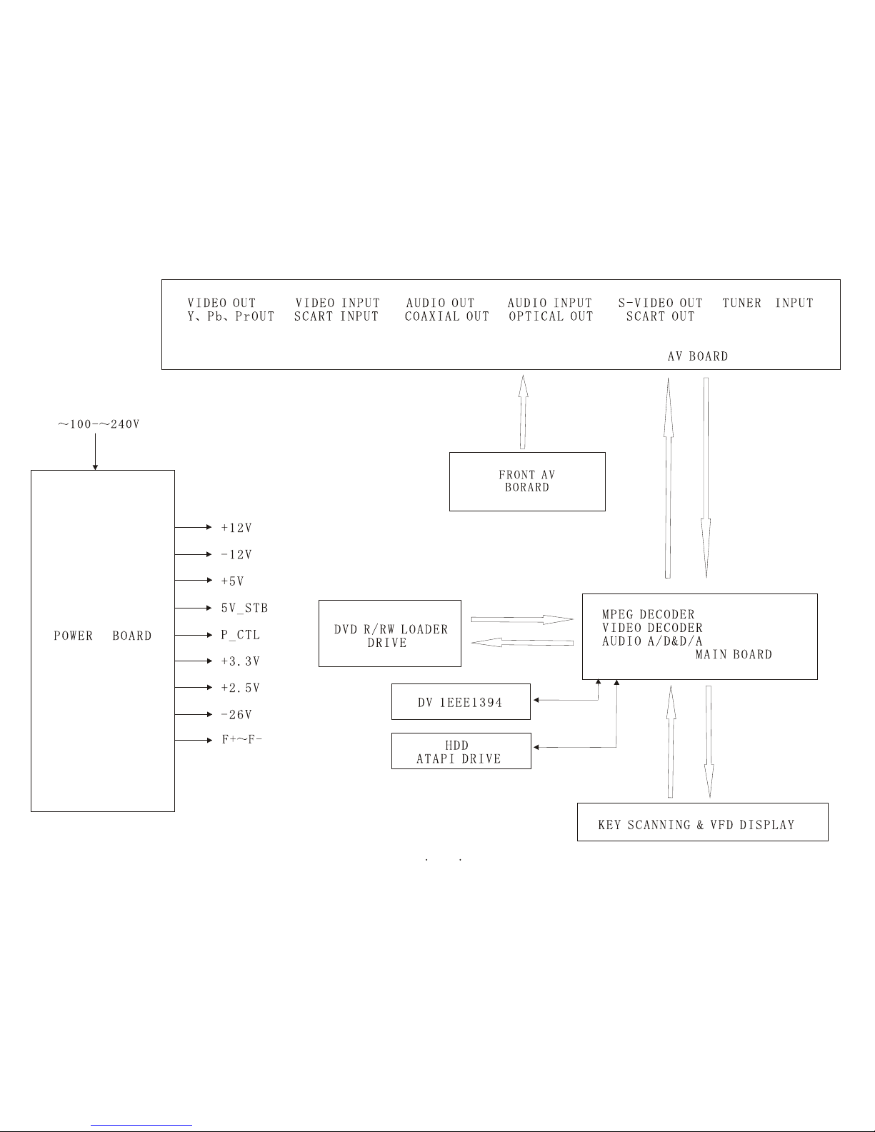
BLOCK DIAGRAM
...................................................................................................................
BLOCK DIAGRAM
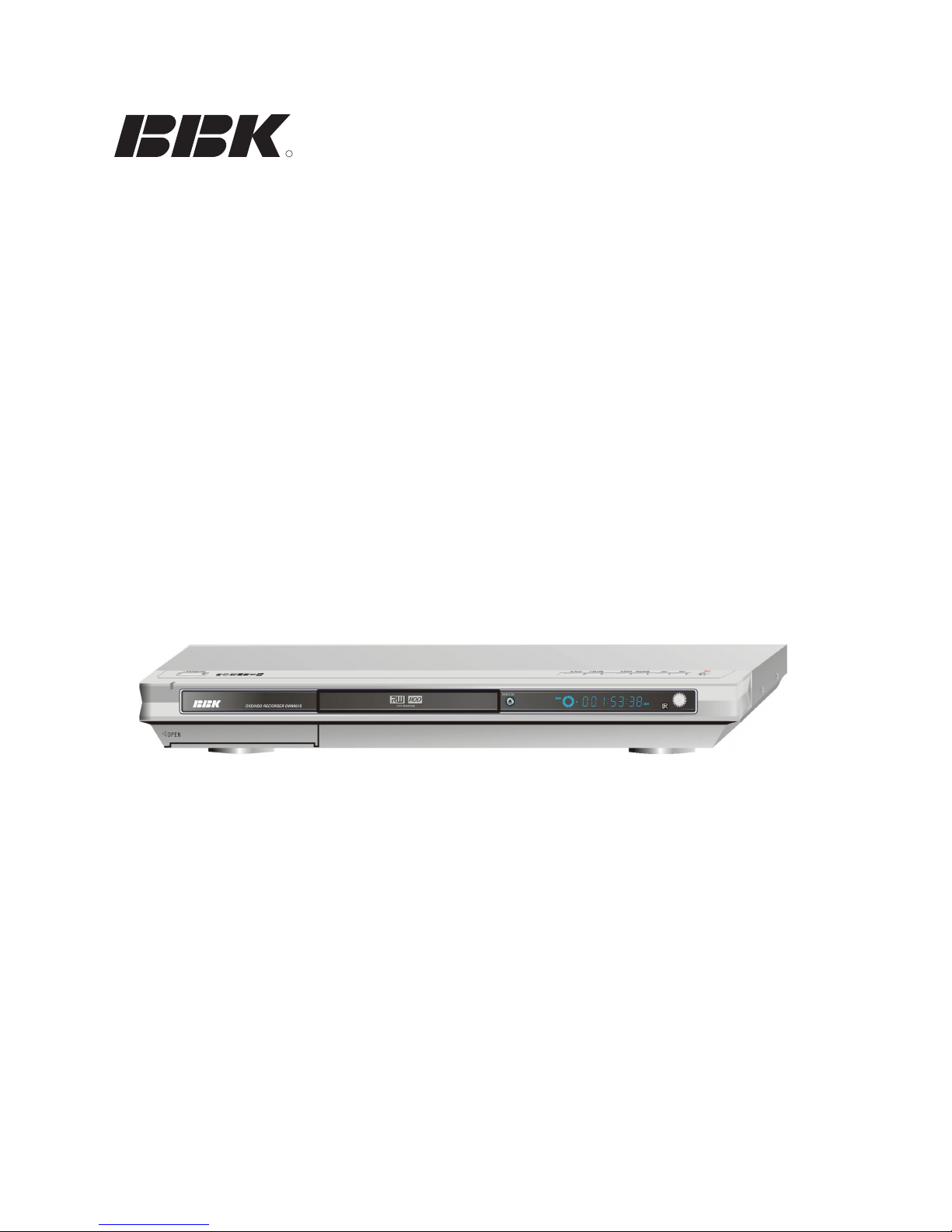
PREFACE
FEATURES
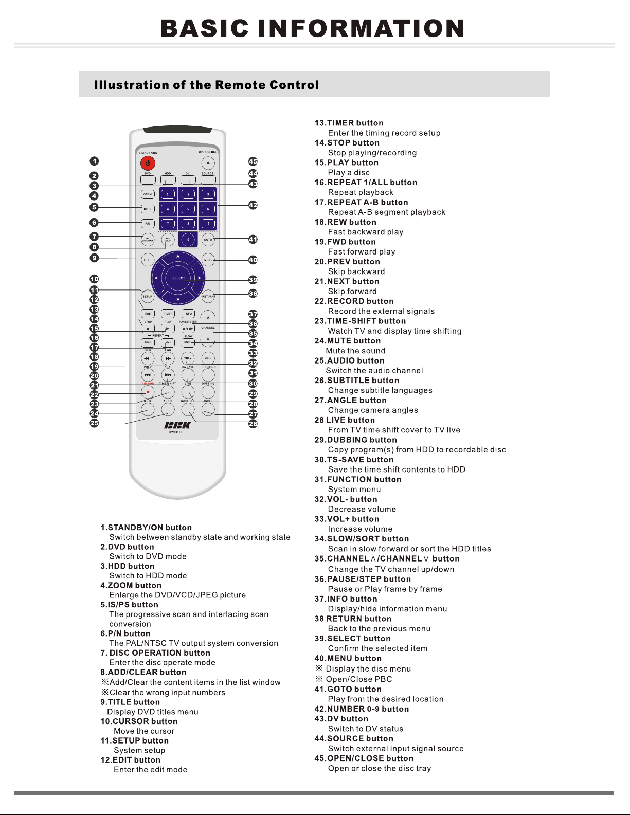
FRONT PANEL&REAR PANEL
REMOTE CONTROL ........................................................................................................................
...................................................................................................................................
..................................................................................................
SCHEMATIC DIAGRAM&PCB SILKSCREEN
MAIN BOARD SCHEMATIC AND PCB LAYOUT 25-39
AV BOARD SCHEMATIC AND PCB LAYOUT 40-51
52-56
KEY BOARD SCHEMATIC AND PCB LAYOUT
POWER BOARD SCHEMATIC AND PCB LAYOUT
...........................................................
...............................................................
.................................................................
...............................................................
57-59
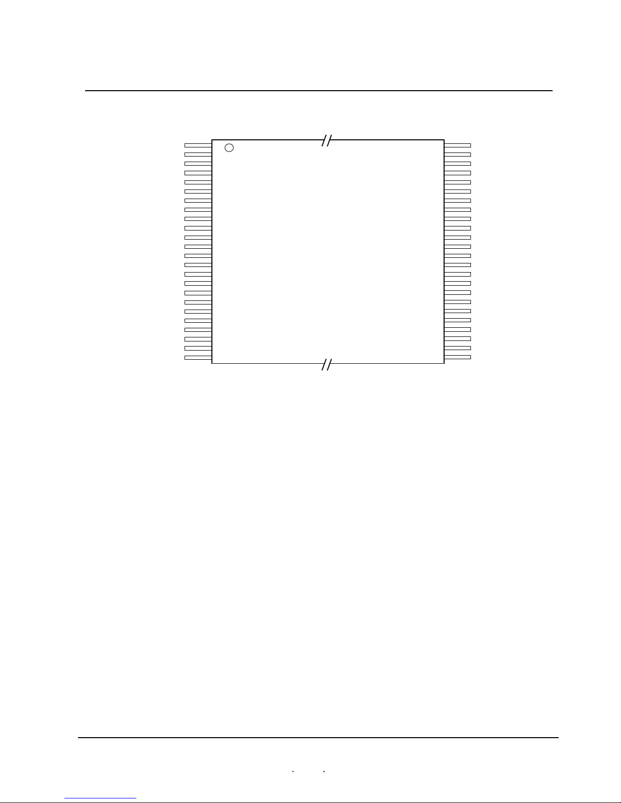
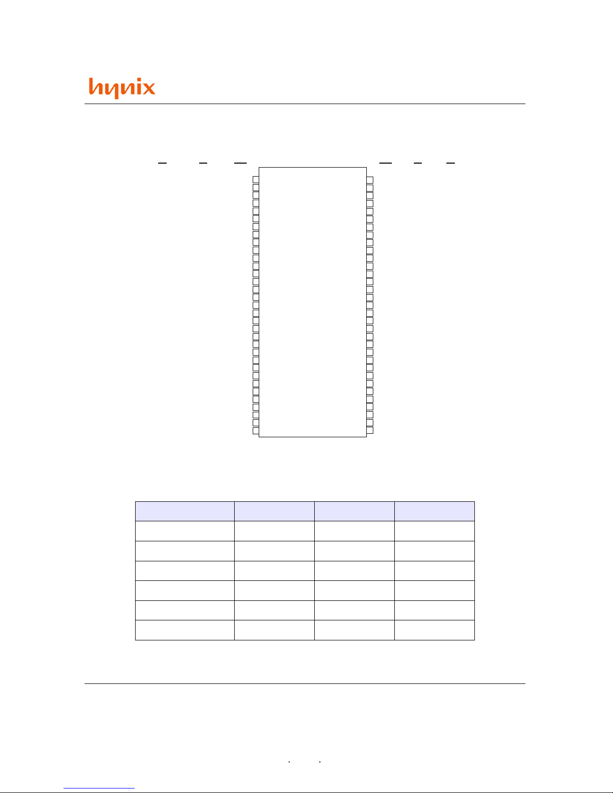
PARTS SPECIFICATIONS
SST39VF3201 ..................................................................................................................................
HY5DU561622CT .............................................................................................................................
TSB41AB1
..........................................................................................................
TVP5146
...........................................................................................................................
CS4360 ...................................................................................................................
CS5333 .............................................................................................................................................
74HC/HCT14 ..................................................................................................................................
74ALVT16373...........................................................................................................................
MM1221~MM1228 .................................................................................................................................
LP2995
.......................................................................................................................
PQXXXEZ02Z ..................................................................................................................................
MSP 34x5G
................................................................................................................
TUNER ...................................................................................................................
PARTSLIST
MAIN BOARD..................................................................................................................................
.......................................................................................................................................
.........................................................................................................................
..............................................................................................................
60-62
MAIN KEY BOARD
......................................................................................................................................
63
POWER BOARD
................................................................................................................
64-65
AV BOARD ............................................................................................................................................ 66-67
POWER SWITCH BOARD 68
DV BOARD 69
..............................................................................................................................
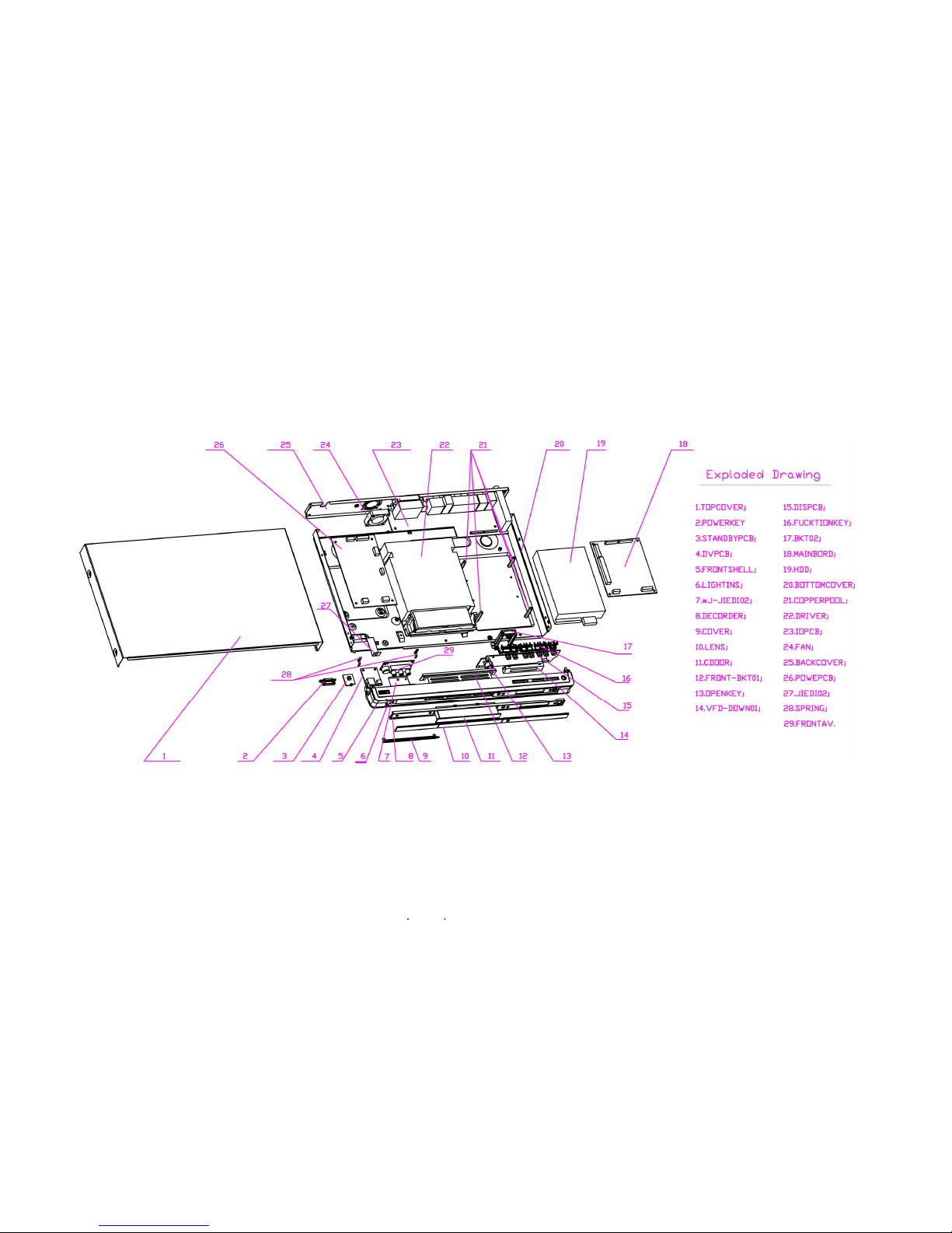
EXPLODED VIEW
EXPLODED VIEW
BLOCK DIAGRAM
6
7
8
9-12
13-14
15-16
17
18
19-20
21
22
23
24
1
2
3
5
4
BLOCK DIAGRAM
FRONT AV BOARD 70