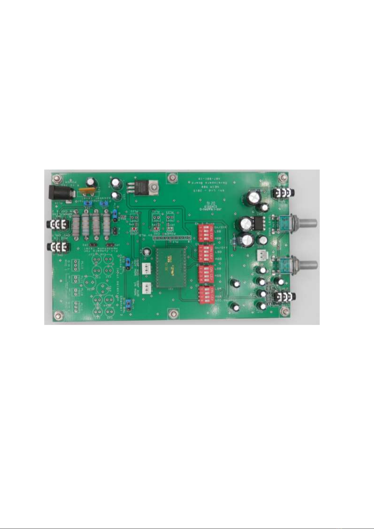
NEDSP900 Development Board
3
1.0 Introduction
The NEDSP900 is a dual channel audio DSP Noise Suppression pcb module for improving the speech
quality in Voice communication systems used in noisy environments. It is capable of handling a wide
range of audio inputs and providing up to 40dB of noise suppression. The module operates on a single
supply rain with on‐board voltage regulation and clock oscillator. It has low power consumption which
makes it suitable for portable applications.
The module has a 26 pin Dual-in-line format with 2mm pin spacing allowing it to ‘plug-in’ to a standard
2mm pitch socket strip.
The NEDSP900 development board was to aid the design-in of the NEDSP900 module. The board allows
various signals to be input to the module and then provides both a Line Out and a Headphone/Small
speaker output to evaluate the processed signal.
Parts of the board have not been populated, but Circuits, Bills of Material (BOM) and information as to
what components fit in these areas are given for the user to add to whatever level they require. This
information can be found throughout this document, but specifically in Section 7.0 and the various
Appendices.
The board has been created such that it can be mounted on standard M3 type pillars for ease of use.
However the format also allows a standard extruded case to be purchased and modified to may this test
board into a robust unit for field testing of the boards’properties.
1.1 Recommendation
We would like to suggest that you just take a few minutes to read through this document first
prior to using the eval board. Some comments have been highlighted in bold,which you should
consider before you connect this device up to your system.
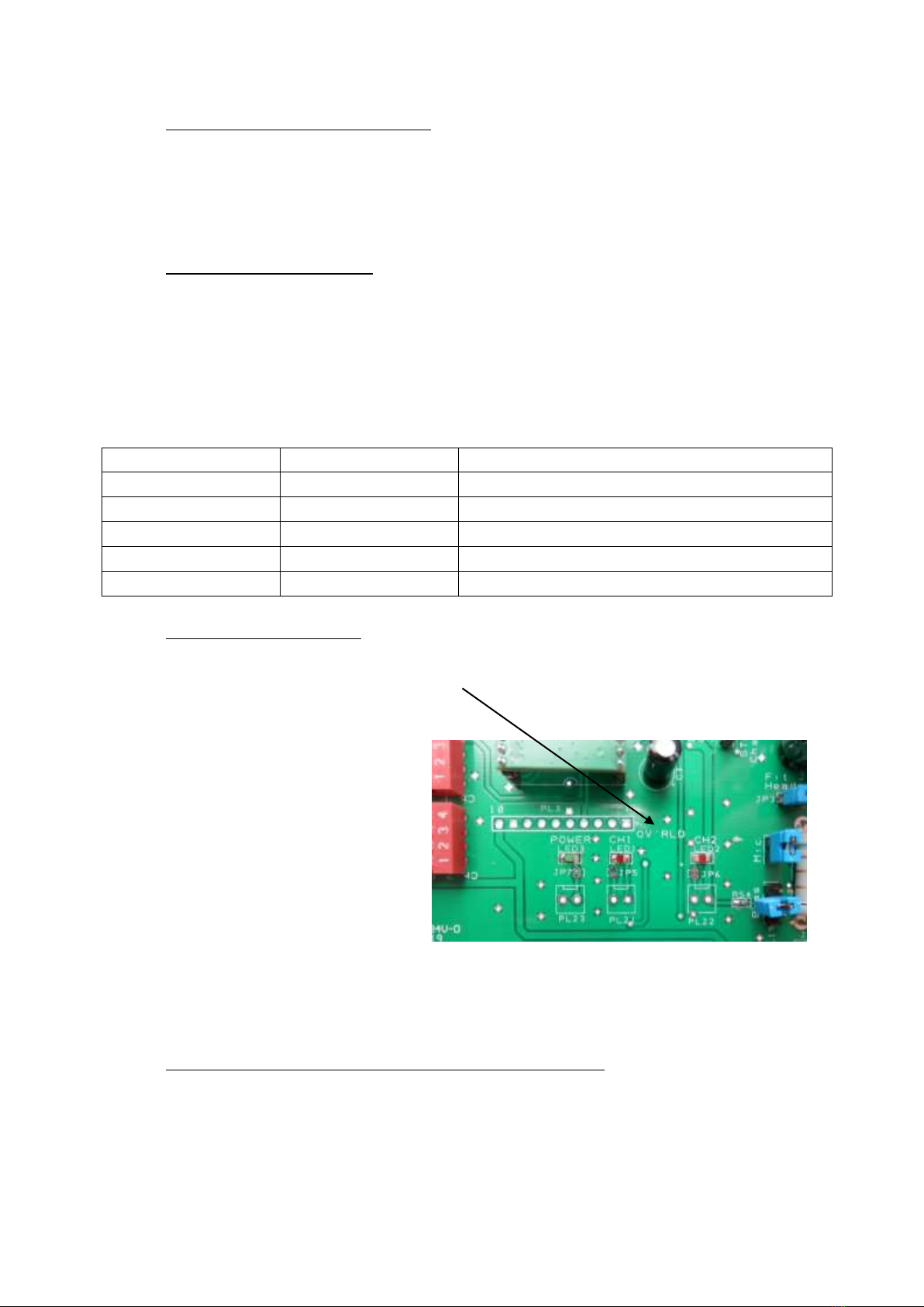
1.2 Board Mechanics
The PCB is approximately 99.5 mm x 159.5 mm and is supplied with M3 x 10mm standoffs as
supports (in 6 positions, see diagram overleaf). These allow components on the underside of the
board to clear the bench. If the PCB is to be fitted into an enclosure, these standoffs may be
used for this purpose or exchanged for shorter ones.
An extruded case can be used to house this board. This provides plenty of room for the board
plus protection for initial system integration when carrying out larger projects. Information
regarding this case and an alternative, if other supplementary circuitry is to be built in, is given
in Appendix C. Drilling patterns for both the front and back covers can also be found in
Appendix C.