Quark Up R1270 - R1270CEVB - Technical Information Manual
Index …
Scope of Manual............................................................................................................................................................................. 2
Change Document Record.............................................................................................................................................................. 2
Reference Document......................................................................................................................................................................2
Index … ......................................................................................................................................................................................................4
List of Figures.............................................................................................................................................................................................5
List of Tables..............................................................................................................................................................................................5
1Introduction ...................................................................................................................................................................................6
General Information.......................................................................................................................................................................7
Rea der................................................................................................................................................................................7
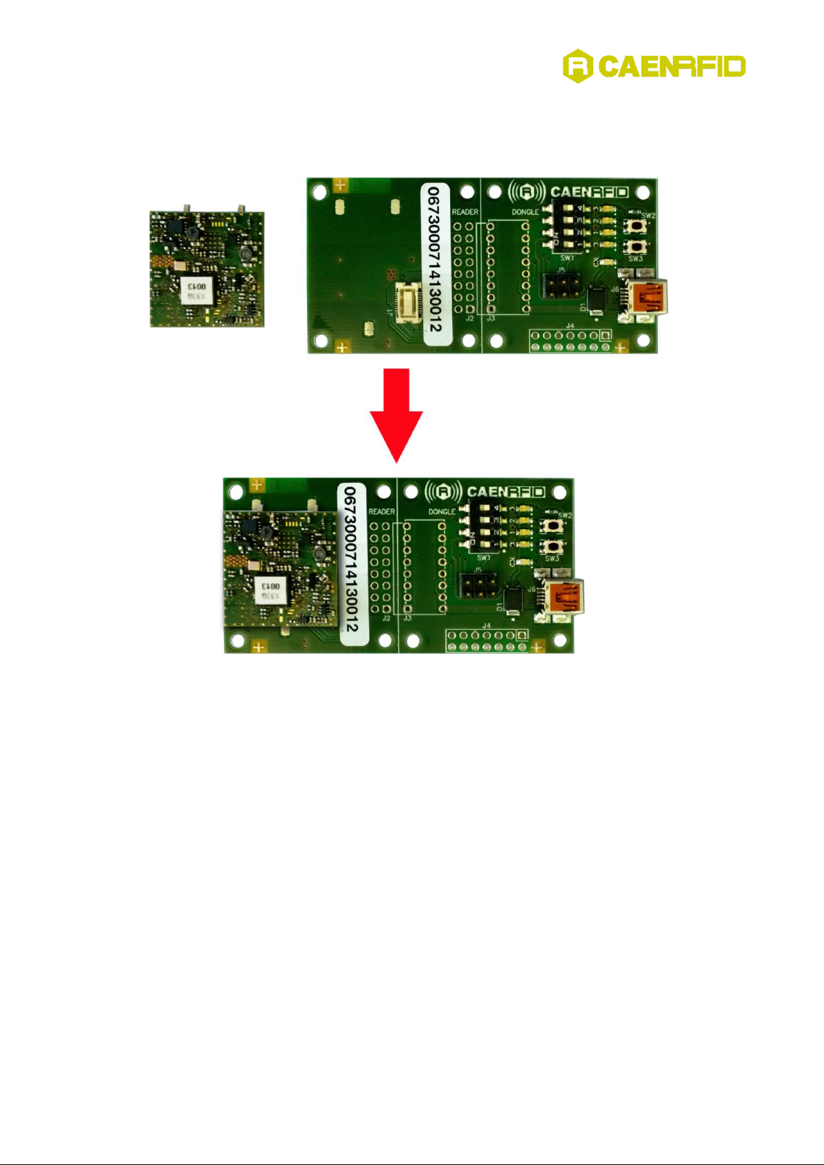
Evaluation Board................................................................................................................................................................ 7
Accessories .....................................................................................................................................................................................8
R1270 Quark Up ReaderAccessories .................................................................................................................................8
R1270CEVB Quark Up Evaluation Board Accessories........................................................................................................8
Development Ki t.............................................................................................................................................................................9
Orderi ng Options............................................................................................................................................................................9
Installation Noti ce ........................................................................................................................................................................10
2Quark Up R1270...........................................................................................................................................................................11
Technical Speci fications Table...................................................................................................................................................... 12
External Connections....................................................................................................................................................................13
R1270 s upply and I/O connector electri cal chara cteris tics.............................................................................................15
Power supply connection ................................................................................................................................................16
General purpose I/O connecti ons ...................................................................................................................................17
External reset...................................................................................................................................................................17
UART connection ............................................................................................................................................................. 18
USB connecti on................................................................................................................................................................ 19
Antenna port specifications.............................................................................................................................................19
Rea der –Tag Link Profiles ............................................................................................................................................................20
Fi rmwa re Upgrade........................................................................................................................................................................20
BSL opera tion...................................................................................................................................................................20
Fi rmwa re upgrade via R1270CEVB board........................................................................................................................21
PCB Pad Layout............................................................................................................................................................................. 23
3Quark Up R1270CEVB ..................................................................................................................................................................24
Technical Speci fications Table...................................................................................................................................................... 25
Connection diagra m.....................................................................................................................................................................25
Installation Noti ce ........................................................................................................................................................................26
Technical drawings .......................................................................................................................................................................26
Electri cal scheme..........................................................................................................................................................................27
External Connections....................................................................................................................................................................28
Installing the USB Vi rtual COM port dri ver ..................................................................................................................................29