Cal Power TrueWave TW5250 User manual

Contact Information
Telephone: 800 733 5427 (toll free in North America)
858 450 0085 (direct)
Fax: 858 458 0267
Email:
Domestic Sales: domorders.sd@ametek.com
International Sales: intlorders.sd@ametek.com
Web: www.programmablepower.com
TrueWave
™
Switching Amplifier
Service Manual
Models:
TW5250
TW3500
TW1750
This Service Manual is incomplete without the
TrueWave Operation Manual, which contains
detailed descriptions of the TrueWave system,
installation instructions, and operating instructions.
March 2011 Document No. M161469-03 Rev C
Via Acquanera, 29 22100 Como
tel. 031.526.566 (r.a.) fax 031.507.984
info@calpower.it www.calpower.it


i
About AMETEK
AMETEK Programmable Power, Inc., a Division of AMETEK, Inc., is a global leader in the design
and manufacture of precision, programmable power supplies for R&D, test and measurement,
process control, power bus simulation and power conditioning applications across diverse
industrial segments. From bench top supplies to rack-mounted industrial power subsystems,
AMETEK Programmable Power is the proud manufacturer of Elgar, Sorensen, California
Instruments and Power Ten brand power supplies.
AMETEK, Inc. is a leading global manufacturer of electronic instruments and electromechanical
devices with annualized sales of $2.5 billion. The Company has over 11,000 colleagues working
at more than 80 manufacturing facilities and more than 80 sales and service centers in the United
States and around the world.
Trademarks
AMETEK is a registered trademark of AMETEK, Inc.
Other trademarks, registered trademarks, and product names are the property of their respective
owners and are used herein for identification purposes only.
Notice of Copyright
TrueWave Switching Amplifier, Service Manual
© 2010 AMETEK Programmable Power, Inc. All
rights reserved.
Exclusion for Documentation
UNLESS SPECIFICALLY AGREED TO IN WRITING, AMETEK PROGRAMMABLE POWER, INC.
(“AMETEK”):
(a) MAKES NO WARRANTY AS TO THE ACCURACY, SUFFICIENCY OR SUITABILITY OF ANY
TECHNICAL OR OTHER INFORMATION PROVIDED IN ITS MANUALS OR OTHER
DOCUMENTATION.
(b) ASSUMES NO RESPONSIBILITY OR LIABILITY FOR LOSSES, DAMAGES, COSTS OR
EXPENSES, WHETHER SPECIAL, DIRECT, INDIRECT, CONSEQUENTIAL OR INCIDENTAL,
WHICH MIGHT ARISE OUT OF THE USE OF SUCH INFORMATION. THE USE OF ANY SUCH
INFORMATION WILL BE ENTIRELY AT THE USER’S RISK, AND
(c) REMINDS YOU THAT IF THIS MANUAL IS IN ANY LANGUAGE OTHER THAN ENGLISH,
ALTHOUGH STEPS HAVE BEEN TAKEN TO MAINTAIN THE ACCURACY OF THE
TRANSLATION, THE ACCURACY CANNOT BE GUARANTEED. APPROVED AMETEK CONTENT
IS CONTAINED WITH THE ENGLISH LANGUAGE VERSION, WHICH IS POSTED AT
WWW.PROGRAMMABLEPOWER.COM.
Date and Revision
March 2011 Revision C
Part Number
M161469-03
Contact Information
Telephone: 800 733 5427 (toll free in North America)
858 450 0085 (direct)
Fax: 858 458 0267
Email: sales@programmablepower.com
service@programmablepower.com
Web: www.programmablepower.com

ii
This page intentionally left blank.

iii
Important Safety Instructions
Before applying power to the system, verify that your product is configured properly for your
particular application.
WARNING
Hazardous voltages may be present when covers are removed. Qualified
personnel must use extreme caution when servicing this equipment.
Circuit boards, test points, and output voltages also may be floating above
(below) chassis ground.
WARNING
The equipment used contains ESD sensitive ports. When installing
equipment, follow ESD Safety Procedures. Electrostatic discharges might
cause damage to the equipment.
Only qualified personnel who deal with attendant hazards in power supplies, are allowed to perform
installation and servicing.
Ensure that the AC power line ground is connected properly to the Power Rack input connector or
chassis. Similarly, other power ground lines including those to application and maintenance
equipment must be grounded properly for both personnel and equipment safety.
Always ensure that facility AC input power is de-energized prior to connecting or disconnecting any
cable.
In normal operation, the operator does not have access to hazardous voltages within the chassis.
However, depending on the user’s application configuration, HIGH VOLTAGES HAZARDOUS TO
HUMAN SAFETY may be normally generated on the output terminals. The customer/user must
ensure that the output power lines are labeled properly as to the safety hazards and that any
inadvertent contact with hazardous voltages is eliminated.
Guard against risks of electrical shock during open cover checks by not touching any portion of the
electrical circuits. Even when power is off, capacitors may retain an electrical charge. Use safety
glasses during open cover checks to avoid personal injury by any sudden component failure.
Neither AMETEK Programmable Power Inc., San Diego, California, USA, nor any of the subsidiary
sales organizations can accept any responsibility for personnel, material or inconsequential injury,
loss or damage that results from improper use of the equipment and accessories.
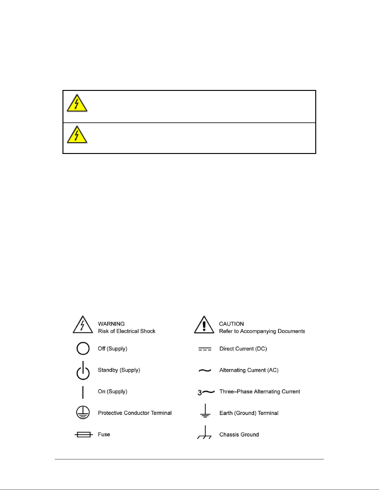
SAFETY SYMBOLS

iv
Product Family: Models: TW5250, TW3500, TW1750
Warranty Period: One Year
WARRANTY TERMS
AMETEK Programmable Power, Inc. (“AMETEK”), provides this written warranty covering the
Product stated above, and if the Buyer discovers and notifies AMETEK in writing of any defect in
material or workmanship within the applicable warranty period stated above, then AMETEK may,
at its option: repair or replace the Product; or issue a credit note for the defective Product; or
provide the Buyer with replacement parts for the Product.
The Buyer will, at its expense, return the defective Product or parts thereof to AMETEK in
accordance with the return procedure specified below. AMETEK will, at its expense, deliver the
repaired or replaced Product or parts to the Buyer. Any warranty of AMETEK will not apply if the
Buyer is in default under the Purchase Order Agreement or where the Product or any part
thereof:
is damaged by misuse, accident, negligence or failure to maintain the same as
specified or required by AMETEK;
is damaged by modifications, alterations or attachments thereto which are not
authorized by AMETEK;
is installed or operated contrary to the instructions of AMETEK;
is opened, modified or disassembled in any way without AMETEK’s consent; or
is used in combination with items, articles or materials not authorized by AMETEK.
The Buyer may not assert any claim that the Products are not in conformity with any warranty
until the Buyer has made all payments to AMETEK provided for in the Purchase Order Agreement.
PRODUCT RETURN PROCEDURE
1. Request a Return Material Authorization (RMA) number from the repair facility (must be
done in the country in which it was purchased):
In the USA, contact the AMETEK Repair Department prior to the return of the
product to AMETEK for repair:
Telephone: 800-733-5427, ext. 2295 or ext. 2463 (toll free North America)
858-450-0085, ext. 2295 or ext. 2463 (direct)
Outside the United States, contact the nearest Authorized Service Center
(ASC). A full listing can be found either through your local distributor or our
website, www.programmablepower.com, by clicking Support and going to the
Service Centers tab.
2. When requesting an RMA, have the following information ready:
Model number
Serial number
Description of the problem
NOTE: Unauthorized returns will not be accepted and will be returned at the shipper’s expense.
NOTE: A returned product found upon inspection by AMETEK, to be in specification is subject to
an evaluation fee and applicable freight charges.

v
TABLE OF CONTENTS
Warranty.........................................................................................................................i
Safety Notice.................................................................................................................iii
Safety Symbols............................................................................................................ iv
SECTION 1 –THEORY OF OPERATION
1.1 INTRODUCTION...............................................................................................1-1
1.2 SYSTEM OVERVIEW.......................................................................................1-1
1.3 INTERCONNECTION .......................................................................................1-3
1.4 DIGITAL CONTROL BOARD............................................................................1-4
1.5 ANALOG PROCESSOR BOARD......................................................................1-6
1.6 HOUSEKEEPING BOARD (HSKP)...................................................................1-7
1.7 POWER CONDITIONER MODULE..................................................................1-8
1.7.1 RECTIFIER INPUT..............................................................................1-8
1.7.2 POWER FACTOR CORRECTION (PFC) INPUT................................1-8
1.7.3 DC/DC CONVERTER..........................................................................1-9
1.8 AMPLIFIER MODULE.......................................................................................1-9
1.9 GLOSSARY.....................................................................................................1-10
SECTION 2 –MAINTENANCE AND TROUBLESHOOTING
2.1 GENERAL ........................................................................................................2-1
2.2 FACTORY REPAIR..........................................................................................2-1
2.3 REQUIRED TEST EQUIPMENT......................................................................2-2
2.4 PERIODIC MAINTENANCE.............................................................................2-2
2.5 FAULT SYMPTOMS/TROUBLESHOOTING ..................................................2-3
2.6 DISASSEMBLY & RE-ASSEMBLY ..................................................................2-5

TABLE OF CONTENTS TW SERIES
vi
SECTION 3 –CALIBRATION
3.1 SCOPE............................................................................................................. 3-1
3.2 APPLICABLE DOCUMENTS........................................................................... 3-1
3.3 REQUIRED TEST EQUIPMENT......................................................................3-1
3.4 SETUP............................................................................................................. 3-2
3.5 CALIBRATION RESET.................................................................................... 3-2
3.6 DC OFFSET CALIBRATION............................................................................ 3-3
3.7 DC LOCAL LOW RANGE CALIBRATION....................................................... 3-4
3.8 DC LOCAL HIGH RANGE CALIBRATION....................................................... 3-6
3.9 DC REMOTE LOW RANGE CALIBRATION.................................................... 3-8
3.10 DC REMOTE HIGH RANGE CALIBRATION................................................... 3-9
3.11 LOCAL LOW RANGE FREQUENCY CALIBRATION....................................3-11
3.12 LOCAL HIGH RANGE FREQUENCY CALIBRATION ................................... 3-14
3.13 REMOTE LOW RANGE FREQUENCY CALIBRATION ................................ 3-16
3.14 REMOTE HIGH RANGE FREQUENCY CALIBRATION................................ 3-19
3.15 EXTERNAL PHASE REFERENCE CALIBRATION....................................... 3-22
3.16 PHASE A TO PHASE B CALIBRATION........................................................ 3-23
3.17 PHASE A TO PHASE C CALIBRATION........................................................3-25
3.18 EXTERNAL GAIN CONTROL CALIBRATION...............................................3-27
3.19 LOW RANGE CURRENT CALIBRATION...................................................... 3-28
3.20 LOCAL LOW RANGE WATTS CALIBRATION.............................................. 3-29
3.21 REMOTE LOW RANGE WATTS CALIBRATION.......................................... 3-30
3.22 LOW RANGE CURRENT FREQUENCY CALIBRATION .............................. 3-31
3.23 LOCAL LOW RANGE WATTS FREQUENCY CALIBRATION ......................3-33
3.24 REMOTE LOW RANGE WATTS FREQUENCY CALIBRATION................... 3-34
3.25 HIGH RANGE CURRENT CALIBRATION..................................................... 3-36
3.26 LOCAL HIGH RANGE WATTS CALIBRATION............................................. 3-37
3.27 REMOTE HIGH RANGE WATTS CALIBRATION ......................................... 3-38
3.28 HIGH RANGE CURRENT FREQUENCY CALIBRATION.............................. 3-39
3.29 LOCAL HIGH RANGE WATTS FREQUENCY CALIBRATION...................... 3-40
3.30 REMOTE HIGH RANGE WATTS FREQUENCY CALIBRATION.................. 3-42

SERVICE MANUAL TABLE OF CONTENTS
vii
SECTION 4 –PARTS LIST
4.1 GENERAL ........................................................................................................4-1
4.2 PARTS LIST.....................................................................................................4-1
4.3 ORDERING SPARE PARTS............................................................................4-2
SECTION 5 –DIAGRAMS
5.1 GENERAL ........................................................................................................5-1
5.2 DIAGRAMS ......................................................................................................5-1
LIST OF FIGURES
FIGURE 1-1TW 5250...........................................................................................1-2
FIGURE 1-2DIGITAL CONTROL BOARD BLOCK DIAGRAM ............................1-4
FIGURE 1-3ANALOG PROCESSOR BOARD BLOCK DIAGRAM......................1-6
FIGURE 1-7POWER CONDITIONER MODULE BLOCK DIAGRAM...................1-8
LIST OF TABLES
TABLE 2-1REQUIRED TEST EQUIPMENT........................................................2-2
TABLE 2-2FUSES................................................................................................2-3
TABLE 2-3TROUBLESHOOTING........................................................................2-4
TABLE 3-1CALIBRATION TEST EQUIPMENT...................................................3-1
TABLE 4-1PARTS LIST.......................................................................................4-1
TABLE 5-1TRUEWAVE SYSTEM DIAGRAMS ...................................................5-1

TABLE OF CONTENTS TW SERIES
viii
This page intentionally left blank.

1-1
SECTION 1 –THEORY OF OPERATION
1.1 INTRODUCTION
This service manual is intended to assist in the maintenance, troubleshooting, repair
to the module level, and calibration of the Elgar TrueWave (TW) products. The topics
discussed in this manual may require a level of understanding of analog and digital
circuit theory somewhat higher than that required for normal Operator/Programmer
activities. For this reason, only qualified personnel should attempt to troubleshoot and
repair TrueWave products.
This section describes the TW Power Sources and associated circuit boards,
assemblies and interconnecting signals. Topics of this section provide a basis for
understanding the roles performed by the system electronics and should be a precursor
to any troubleshooting or maintenance.
Prior to the module level discussion of the assemblies and boards within the TW
system, a top-level system overview is provided. An understanding of both top level and
circuit activities at the module or board level is most valuable should the service person
find it necessary to investigate a suspected fault or malfunction within the power source.
1.2 SYSTEM OVERVIEW
Figure 1-1 shows a simplified block diagram of the TW system. The 3 phase input
voltage is delivered via the input filter to the power module(s) where it is rectified
providing bus voltages for the amplifier(s). Voltage and waveform control signals are
delivered to the amplifier(s) from the front panel assembly. The front panel assembly
contains the Digital Control Board, and the Analog Processor Board (see sections 1.4
and 1.5). From the bus voltages and control signals, the amplifiers then produce output
waveforms, which are delivered via the output filter to the output terminals.
There are three primary options that are available when ordering a TW system, which
with all permutations considered, translates into many different configurations of TW
systems. The options are: PFC or rectifier input, 208VAC or 400VAC input voltage,
power rating of the unit (number of phases installed).
The PFC/rectifier and input voltage options will be discussed in more detail later in this
manual.

THEORY OF OPERATION TW SERIES
1-2
FIGURE 1-1. TW5250
PWR MOD: ØA
RECTIFIER
-OR-
PFC DC/DC
PWR MOD: ØB
RECTIFIER
-OR-
PFC DC/DC
PWR MOD: ØC
RECTIFIER
-OR-
PFC DC/DC
BACKPLANE
AMPLIFIER: ØA
AMPLIFIER: ØB
AMPLIFIER: ØC
+290VDC BUS
-290VDC BUS
+290VDC BUS
-290VDC BUS
+290VDC BUS
-290VDC BUS
BACKPLANE
OUTPUT FILTER
• • •
INPUT
FILTER
•••
•••
3Ø
INPUT
208 VAC
-OR-
400 VAC
(W/NEUTRAL)
ØA OUT
ØB OUT
ØC OUT
ANALOG
PROCESSOR
BOARD
DIGITAL
CONTROL
BOARD
FRONT
PANEL
DISPLAY
AND
CONTROL

SERVICE MANUAL THEORY OF OPERATION
1-3
The system shown in Figure 1-1 is a TW5250 meaning that it contains three identical
output channels A, B, and C, with a channel consisting of a power module and an
amplifier module. Each channel is capable of delivering 1750 VA to the output. One and
two channel systems, TW1750 and TW3500, can be achieved by removing channels B
and C, or C only (Note: adding or removing a channel requires reprogramming of the
system). TW10500, TW15750, and TW21000 systems can be produced by adding
additional TW chassis.
1.3 INTERCONNECTION
The 3 phase input voltage is delivered via the fuse block and input filter to the power
module(s), through W1, 2 and 3, where it is rectified via the PFC or rectifier input
stage(s). The rectified voltages are then delivered to the DC/DC converter(s) where
290V buses are produced and delivered via the backplane board to the amplifier(s). A
48V bus is also produced by the DC/DC converter(s) and delivered via the backplane to
the HSKP board (see section 1.6). The amplifier(s) receive waveform drive signals and
power supply voltages via ribbon cables and a signal routing board. The Digital Control
Board receives external input locally from the front panel keypad or remotely from the
RS232 or GPIB (IEEE 488.2). The Digital Control Board then sends data and
commands to the Analog Processor Board with the desired waveform information to
drive the amplifiers as mentioned above.

THEORY OF OPERATION TW SERIES
1-4
1.4 DIGITAL CONTROL BOARD
FIGURE 1-2. DIGITAL CONTROL BOARD BLOCK DIAGRAM
The Digital Control Board is the central controller of the TW system. It handles all
communication with the outside world and the Analog Processor Board. It consists of
the following interfaces:
• Front panel keypad and display elements
• GPIB (IEEE 488.2 interface) SCPI Protocol
• RS-232 (9600 baud, 1 start bit, 8 data bit, no parity, 1 stop bit) SCPI Protocol
• QSPI for Analog Processor Board interface
The Digital Control Board is controlled by a Motorola 68332 processor, operating with a
16-bit data bus. The processor system memory consists of one 256K x 16 20ns static
RAM, one 256K x 16 90ns FLASH ROM, 64K x 8 120ns PROM and 8K x 8 EEPROM.
The PROM is used during boot for processor execution, the EEPROM is used for
calibration data, the FLASH is used for processor execution, and the RAM is used for
system data storage. For more information on the MC68332 processor, refer to the
Motorola MC68332 User’s Manual.
At power up the 68332 boots from a dedicated PROM. This PROM contains
executable code that allows the FLASH memory to be programmed from data received
either from the GPIB or serial port. During the boot process the FLASH memory is
KEYPAD
DISPLAY
GPIB
RS-232
MC68332
PROCESSOR
SYSTEM
MEMORY
QSPI Analog
Processor
Board

SERVICE MANUAL THEORY OF OPERATION
1-5
checked for corruption, and if no corruption is found program control is passed to the
FLASH memory.
The Digital Control Board communicates to the Analog Processor Board via the 68332
processor’s dedicated high speed QSPI. The Digital Control Board is the master in this
interface. Upon power-up of the TW system, the Digital Control Board performs the
following functions:
• Initializes all chip selects, PortE and PortF of the 68332 processor.
• Initializes the QSPI, QSCI, TPU, GPIB, display and keypad.
• Resets and loads run-time DSP code to the Analog Processor Board.
• Initializes Analog Processor Board to front panel settings.
• Programs the amplifier(s) to power-on reset values
(either default or user defined values).
• Performs system self test.
• Enters main control loop.
The main control loop reads the keypad for user input, updates the displays and data
buffers with current readback values from the Analog Processor Board, and interprets
SCPI strings received from either the RS-232 or GPIB bus. Additionally, the Analog
Processor Board is monitored for fault conditions. If a fault occurs, the fault is logged to
the front panel display and the appropriate fault buffer is generated for the remote
interfaces.
All calibration data is stored on the Digital Control Board. When an incoming SCPI
command or front panel programming value is processed, the appropriate calibration
data are applied to the value and the information is passed to the Analog Processor
Board for implementation. The TW relies heavily on software calibration and a detailed
calibration procedure can be found in section 3 of this manual.

THEORY OF OPERATION TW SERIES
1-6
1.5 ANALOG PROCESSOR BOARD
FIGURE 1-3. ANALOG PROCESSOR BOARD BLOCK DIAGRAM
The Analog Processor Board generates the three–phase sinewave references, signal
processes the sampled currents and voltages, performs output voltage servoing, and
drives the power amplifiers. Additionally the Analog Processor Board has a power
supply that provides fan power and front panel power.
Processing power is provided by a TMS320C50 digital signal processor (DSP). The
DSP’s firmware is loaded into the processor at power up from the Digital Control Board.
After initializing all registers and calibrating the analog to digital converter, the DSP
enters its main control loop. All waveform generation and measurements are handled
by the DSP. Current mode of operation is also controlled by the DSP. Hardware faults
are monitored by the DSP and appropriate actions are taken by the DSP when a fault
occurs.
The sinewave references are constructed using three waveform DACs and one
amplitude DAC driving the voltage reference. The DSP updates each of the waveform
DACs every 37.5 microseconds with the appropriate amplitude value for the phase
waveform being constructed. The output of the DACs are filtered by a 5 pole waveform
construction filter to eliminate any steps in the waveform. The amplitude DAC is
updated as necessary to set the maximum peak to peak output voltage generated by
the TW.
Digital
Control
Board
TMS320C50
PROCESSOR SERVO
AMPLIFIERS
QSPI
VOLTAGE
DAC
WAVEFORM
DACs
8CHANNEL
ADC
POWER
SUPPLY
POWER
AMPLIFIERS

SERVICE MANUAL THEORY OF OPERATION
1-7
The sinewave references are fed either directly to the servo amplifiers or are AC
coupled, depending on the selected coupling mode of operation. The servo amplifiers
operate on the sinewave reference and the local or remote sense lines. The output of
the servo amplifiers feed the power amplifier drivers. Phases B and C have a mux that
selects between the output of their respective servo amplifiers or phase A’s servo
amplifier. This allows the power supply to operate in multiphase or single–phase mode.
Each power amplifiers current is sampled and processed through a summing bus that
allows multiple TW chassis to be paralleled. This summing bus output is then filtered
and fed into the front end of the eight–channel analog to digital converter. The ADC
also samples sense voltage, redundant over–voltage, and external user input.
The DSP reads one of the eight analog inputs to the ADC once every 12.5
microseconds. The sampled values of voltage and current are processed into RMS
current, RMS voltage, peak current, and instantaneous power. These values are
passed to the Digital Control Board for further calibration scaling and presentation to
the user.
1.6 HOUSEKEEPING BOARD (HSKP)
The HSKP board receives 48Vdc input from the power module(s) via the backplane
board where the 48V inputs are paralleled and delivered via J7A connector to the HSKP
board. The 48V is then delivered to the housekeeping circuit and also via the J3
connector to power the fans of the fan panel assembly. The housekeeping power
supply circuit consists of a push-pull converter producing two non-isolated and five
isolated outputs. These seven output voltages supply power throughout the TW
chassis. The voltages developed by the housekeeping supply are as follows:
• +/-B (+/-13V) supplies (chassis potential): Used to power circuitry at chassis
ground potential throughout the front panel boards.
• +/-15V analog supplies: Used to power circuitry at analog ground potential
throughout the amplifiers and front panel boards.
• +5V & -24V supplies (chassis potential): Used to power circuitry at chassis
ground potential throughout the front panel boards.
• +5V digital supply: Used to power circuitry at digital ground potential throughout
the amplifiers and front panel boards.
Note that the HSKP board does not supply voltages to the PFC, rectifier, or DC/DC
assemblies. For an explanation on how the bus voltages for these assemblies are
supplied, consult the theory of operation for each individual assembly.

THEORY OF OPERATION TW SERIES
1-8
1.7 POWER CONDITIONER MODULE
FIGURE 1-7. POWER CONDITIONER MODULE BLOCK DIAGRAM
The power conditioner module, or power module, rectifies the AC input voltage into one
48 Vdc and two isolated 290 Vdc buses. This is accomplished in two separate stages of
the power module. The first stage (input stage) can consist of either a rectifier or a PFC
stage. Both the rectifier and the PFC input stages are configurable for two different
nominal AC input voltages: 208VAC L-L (USA) or 400VAC L-L (INTERNATIONAL). For
further information on configuring input voltages, contact the Elgar Customer Service
Department. The second stage consists of a DC/DC converter module that converts the
380 Vdc output of the input stage to one 48 Vdc and two isolated 290 Vdc buses.
1.7.1 RECTIFIER INPUT
The 3 phase AC input voltage to the rectifier input stage is delivered through a soft-start
circuit and rectified by a 3 phase bridge rectifier developing a 380 Vdc bus. When the
system is configured for USA input, the rectifier is wired as a 3 phase full-wave bridge
rectifier. When the system is configured for INTERNATIONAL input, the rectifier is
wired as a 3 phase half-wave rectifier. The rectified 380 Vdc bus is then delivered to the
DC/DC stage of the power module. The 380 Vdc bus is also used to power a series
regulator circuit, which provides +24 Vdc bus power for the control circuitry of the
rectifier stage.
1.7.2 POWER FACTOR CORRECTION (PFC) INPUT
The PFC module is used to limit the peak input current to the TW system by as much
as three to one, compared to the peak input current of the rectifier module. This
equates to a PFC input power factor of .99, compared to the power factor of the rectifier
module that is .6 (USA) and can be as low as .35 (INTERNATIONAL).
3 Phase
AC Input
Front Panel
On/Off
Switch
PFC
Input
Stage
Rectifier
Input
Stage
DC/DC
Converter
HSKP
Amplifier
POWER
+
48VDC
-290VDC
+290VDC

SERVICE MANUAL THEORY OF OPERATION
1-9
The PFC module is a two–board assembly consisting of a PFC Power and a PFC
Control board. The single–phase AC input voltage enters the PFC power board where it
is rectified by the full-wave bridge rectifier circuit, developing a raw 380 Vdc bus. The
raw 380 Vdc bus is then delivered through a soft–start relay to the PFC circuit, which is
comprised of a boost converter. The output of the PFC, a regulated 380 Vdc bus, is
then delivered to the DC/DC stage of the power module. The 380 Vdc bus is also
converted down to a 24 Vdc bus used to power the control circuitry for the PFC power
and control boards.
CAUTION
When the PFC module is configured for the INTERNATIONAL input
configuration, the input neutral must be connected. Failure to do so
will result in catastrophic damage to the PFC input.
1.7.3 DC/DC CONVERTER
The DC/DC converter module, or just DC/DC, is a two–board assembly consisting of a
DC/DC Converter Power and a DC/DC Converter Control board. The DC/DC serves two
purposes. First, to provide isolation between the 3 phase input voltage and the eventual
output voltage used by the customer. Second, to generate the two isolated 290 Vdc
buses used by the amplifier and a 48 Vdc bus used by the HSKP board and fan panel
assembly. The DC/DC converter circuit is rated for 2000 watts and consists of a PWM
controlled full H-bridge, which chops (switches) the 380 Vdc bus supplied by the
rectifier or PFC input stage at a rate of 140 kHz. The output transformer and three full-
wave bridge rectifier circuits then generate the two 290 Vdc and 48 Vdc buses. The
output transformer and associated rectifier circuitry also produces a 27 Vdc bus which
provides power for the DC/DC PWM control circuit.
1.8 AMPLIFIER MODULE
The amplifier module is a four board assembly consisting of an Amplifier Power, an
Amplifier Control and two Gate Drive boards. The amplifier module is in fact comprised
of two 156 V / 6.5 A amplifiers (upper and lower) which can be series or paralleled by
relay K1 on the Amplifier Power board to produce a single 312 V / 6.5 A or 156 V / 13 A
output. Relay K2 is the amplifier output relay but breaks only the line connection to the
output filter and not the neutral. The drive circuits for K1 and K2 are located on the
amplifier control board and respond to commands from the Analog board. Both the
upper and lower amplifiers consist of identical full H-bridges that vary only in the
method in which the bridge current is measured. The lower bridge uses a shunt resistor
to monitor the bridge current while the upper bridge uses a hall-effect current
transformer to provide isolation.
The amplifier control board contains the PWM circuit that generates the drive
waveforms to the upper and lower H-bridges from the input voltage reference signal
sent by the Analog board and the current feedback signals from the upper and lower
bridges. The amplifier runs at a frequency of 200 kHz, interleaved, which equates to an

THEORY OF OPERATION TW SERIES
1-10
overall switching frequency of 400 kHz. This high switching frequency allows smaller
filtering components to be used in the output filter network. The gate drive boards
provide isolation between the amplifier control and power boards. The amplifier control
board contains supervisory circuitry that monitors the amplifier bus voltages and output
neutral to chassis voltages for overvoltage conditions. Also monitored are amplifier
heatsink temperatures as well as output voltage and current feedback signals, all of
which are reported back to the Analog board.
1.9 GLOSSARY
DAC: Digital to Analog Converter
DC/DC: DC/DC Converter
HSKP: Housekeeping Supply Board
PFC: Power Factor Correction
Power Factor: Ratio of the real or active power (watts) to the apparent power (VA).
PLL: Phase Locked Loop
PWM: Pulse Width Modulator
QSPI: Queued Serial Peripheral Interface
This manual suits for next models
2
Table of contents