Casco Logix MSP430AFE253 Development Board User Guide Rev 1.3
www.cascologix.com Page 2
Table of Contents
1 Revision History ..................................................................................................................................................3
2 Features..............................................................................................................................................................3
3 Board Features ...................................................................................................................................................4
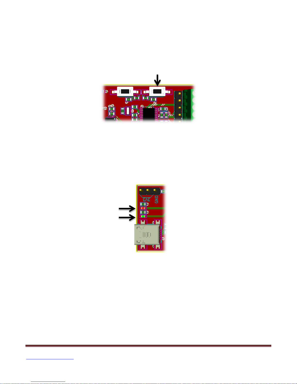
3.1 Mini USB Connector ...................................................................................................................................4
3.2 External Power Connector..........................................................................................................................4
3.3 Analog Connections....................................................................................................................................5
3.4 GPIO Header ...............................................................................................................................................5
3.5 3.3V Jumper................................................................................................................................................6
3.6 TX & RX Jumper ..........................................................................................................................................6
3.7 Spy-by-Wire Debug Header........................................................................................................................6
3.8 Reset Pushbutton .......................................................................................................................................7
3.9 Blue User LED .............................................................................................................................................7
3.10 User Switch 1 ..............................................................................................................................................7
3.11 User Switch 2 ..............................................................................................................................................8
3.12 UART RX & TX LED ......................................................................................................................................8
4 Schematic ...........................................................................................................................................................9
5 PCB Layers ....................................................................................................................................................... 10
6 Bill of Materials................................................................................................................................................ 12