CHIPS HiQVideo Series User manual


Copyright Notice
Copyright1998-99 Intel Corporation (Chips and Technologies, Inc. has been integrated into the Graphics Component Division
(GCD) of Intel Corporation. ALL RIGHTS RESERVED.
This manual is copyrighted by Intel Corporation. You may not reproduce, transmit, transcribe, store in a retrieval system, or
translate into any language or computer language, in any form or by any means - electronic, mechanical, magnetic, optical,
chemical, manual, or otherwise - any part of this publication without the express written permission of Intel Corporation.
Restricted Rights Legend
Use, duplication, or disclosure by the Government is subject to restrictions set forth in subparagraph (c)(1)(ii) of the Rights in
Technical Data and Computer Software clause at 252.277-7013.
Trademark Acknowledgment
CHIPS Logo is a registered trademark of Intel Corporation.
HiQVideo, is a trademark of Intel Corporation.
All other trademarks are the property of their respective holders.
3DQHO/LQN
technology is licensed by Intel Corporation from Silicon Image, Inc. of Palo Alto, CA.
3DQHO/LQN
is a trademark
of Silicon Image, Inc.
Disclaimer
This document provides general information for the customer. Intel Corporation reserves the right to modify the information
contained herein as necessaryand the customer should ensure thatit hasthe mostrecent revision of the document. Intel makes
no warranty for the use of its products and bears no responsibility for any errors which may appear in this document. The cus-
tomer should be on notice that many different parties hold patents on products, components, and processes within the personal
computer industry. Customers should ensure that their use of the products does not infringe upon any patents. Intel respects
the patent rights of third parties and shall not participate in direct or indirect patent infringement.


&+,36
DKHiQV-PCI(Fab.Rev.B)SubjecttoChange WithoutNoticeRevision 1.3 7/2/99
Table of Contents
1.0 Product Description ...............................................................................................................1
2.0 Features ................................................................................................................................2
3.0 Installation .............................................................................................................................3
4.0ABHiQV(Fab Rev.C)&DKHiQV-PCI(Fab Rev.B)Configuration Components.................4
4.1 Configuration Switch (S1) and Jumpers (W1 and W3) .........................................................6
4.2 Push-on Jumpers ..................................................................................................................7
5.0 Connectors ..........................................................................................................................10
6.0 Operation ............................................................................................................................10
6.1 Bus Interface .......................................................................................................................10
6.2 Programmable Linear Acceleration .....................................................................................11
6.3 Memory Interface ................................................................................................................11
6.4 Display Interface .................................................................................................................13
6.4.1 Flat Panel Interface .............................................................................................................13
6.4.2 CRT Interface ......................................................................................................................14
6.5 Clock ...................................................................................................................................16
6.5.1 14MHz Reference Clock .....................................................................................................16
6.5.2 32KHz Clock .......................................................................................................................16
6.6 PCI Configuration ................................................................................................................16
6.7 BIOS Interface .....................................................................................................................16
6.8 NTSC/PAL Composite Video Output (TV out) ....................................................................16
6.9 Multimedia Card Interface ...................................................................................................17
6.10 MPEG and ZV Port Connector ............................................................................................18
6.11 Activity Indicator ..................................................................................................................18
6.12 Mixed Voltage Generation and Power Measurement .........................................................19
6.13 Power Sequencing and Backlight Control ...........................................................................19
6.14 VEESAFE for Panel Operation ...........................................................................................20
6.14.1 Low Voltage for Panel Operation ........................................................................................20
6.14.2 High Voltage Operation for VEESAFE ................................................................................20
6.15
3DQHO/LQN
and LVDS Interfaces ......................................................................................20
7.0 Troubleshooting ..................................................................................................................21

DKHiQV-PCI (Fab. Rev. B) User’s Guide 0
&+,36
DKHiQV-PCI(Fab.Rev.B)SubjecttoChange WithoutNoticeRevision 1.3 7/2/99
List of Figures
Figure 1: Component Location ............................................................................................................4
Figure 2: DKHiQV-PCI based board Jumper Location ........................................................................5
Figure 3: DKHiQV-PCI Flat Panel Connector Pinout .........................................................................13
Figure 4: J11 Connector Pin Assignments ........................................................................................14
Figure 5: Media Connector Pinout .....................................................................................................17
Figure 6: MPEG and ZV Port Connector ...........................................................................................18
List of Tables
Table 1: Configuration Settings ..........................................................................................................6
Table 2: DKHiQV-PCI Jumper Descriptions .......................................................................................7
Table 3: DK Board Connector Functions ..........................................................................................10
Table 4-1: Resistor Connections for EDO Configuration .....................................................................11
Table 4-2: EDO Memory Configuration Types for B65555 ..................................................................12
Table 5: Flat Panel Connection Summary ........................................................................................15
Table 6: Video Sub-System Voltages ...............................................................................................19
Table 7: DKHiQV-PCI (Rev. B) Board Configuration Settings for 69xxx
TV Out and Multimedia Disabled ........................................................................................22
Table 8:ABHiQV(Fab.Rev.C)Daughtercard Configuration Settingsfor 69xxx
TV Out and Multimedia Disabled ........................................................................................23
Table 9: DKHiQV-PCI (Rev. B) Board Configuration Settings for B65555
TV Out and Multimedia Disabled ........................................................................................24
Table 10:ABHiQV(Fab.Rev.C) Daughtercard Configuration Settingsfor B65555
TV Out and Multimedia Disabled ........................................................................................25
Table 11: DKHiQV-PCI Jumper Configuration Settings
for TV Out Enabled on 69xxx and B65555 .........................................................................25
Table 12: DKHiQV-PCI Jumper Configuration Settings for Multimedia Enabled
on 69xxx and B65555 .........................................................................................................26

1 DKHiQV-PCI (Fab. Rev. B) User’s Guide
&+,36
DKHiQV-PCI(Fab.Rev.B)SubjecttoChange WithoutNoticeRevision 1.3 7/2/99
DKHiQV-PCI (Fab. Rev. B)
PCB Design Documentation
1.0 Product Description
The HiQVideoSeries accelerators (65555 and 69xxx) are very high performance LCD/CRT controllers
that provide a complete video subsystem solution with low power consumption, hardware acceleration for
GUI applications and a minimal component count. The high level of integration permits a direct interface to
the PCI Bus and DRAM/SDRAM-based display memory, thus making the HiQVideocontroller a low-cost,
high-performance graphics solution.
The design kits for these products in the PCI bus environment all use a common base board known as the
DKHiQVPCI-based Board. A daughtercard containing the HiQVideo controller is installed onto the main DK
board to complete the design kit. This User’s Guide describes the man DK board. The use of a B65555 or
69xxx HiQVideo accelerator on an ABHiQV daughtercard is also described in the ABHiQV User’s Guide.
The DKHiQVPCI-based board is a full-size PCI add-in card. It has bus connectors to interface with the PCI
Bus at speeds up to 33MHz. The multiple jumper configurations and connectors allow the DK board to test
performance benchmarks, demonstrate various features supported by the HiQVideofamily, measure
power consumption and connect to panels and monitors. Plug-and-Play is possible on the PCI Bus, thus
making PCI easy to use. The PCI autoconfiguration feature determines interrupt setting and software de-
faults. The HiQVideoVGA controllers are mounted on a daughtercard which plugs into a connector on
the DKHiQV-PCI based board to make a complete design kit. This allows the user to exchange silicon sim-
ply by replacing the daughtercard without having to replace the entire kit.
This document describes the revision "B" of the DKHiQV-PCI printed circuit board.

DKHiQV-PCI (Fab. Rev. B) User’s Guide 2
&+,36
DKHiQV-PCI(Fab.Rev.B)SubjecttoChange WithoutNoticeRevision 1.3 7/2/99
2.0 Features
The DKHiQV-PCI has the following features when running a HiQVideocontroller:
• High Performance Flat Panel/CRT GUI Accelerator running on PCI Bus
• Flexible display memory configurations support up to 4MB with a B65555. (The memory resides on the
daughtercard for the B65555.)
• 50-pin flat panel connector for interfacing to most types of flat panels (up to 24 data bits).
• 26-pin flat panel connector for 12 additional data bits for panels having up to a 36-bit data word width
• 15-pin standard VGA connector
• 40-pin MPEG connector for interfacing to an MPEG video card
• Two 25-pin and one 12-pin connector for interfacing to the multimedia daughtercard.
• PCI BIOS ROM support, located on the daughtercard
• Flexible power supplies individually configurable to 3.3V and 5V for different blocks of the video sub-
system
• Onboard power sequencing
• VGA to NTSC/PAL conversion to provide S-VHS video and composite video outputs
• Interrupt signal added for 69xxx support (INT# to INTA on PCI bus)
• TV out and CRT enable/disable under software control
Note: Limited solution, CRT HSYNC/VSYNC only, not RGB
• ACT125 buffer for CSYNC to TV out encoder (AD722) to met Vih spec
• 32 kHz improvement for better rise/fall times
• +5V removed from VCC jumpers; 3.3V-only for VGA controller VCC pins
Note: +5V can be reconnected with only one wire if needed for older products.
• RAMVCC separated from MVCC55X so that +5V can be used for DRAM while using 3.3V for VGA con-
troller VCC
• On daughtercard header, GVCC can be 3.3V instead of 5V to allow 3V EPROM to be used on the
daughtercard if desired
• Four new GND test points have been added and two existing GND points have been moved out from
under the daughtercard to be more accessible
• Low voltage option for VEESAFE (1K pot, fed by VDDSAFE)

3 DKHiQV-PCI (Fab. Rev. B) User’s Guide
&+,36
DKHiQV-PCI(Fab.Rev.B)SubjecttoChange WithoutNoticeRevision 1.3 7/2/99
3.0 Installation
1. Unpack the DKHiQV-PCI (Fab Rev. B) board and visually inspect for any damage that may have
occurred during shipping.
2. Read this DKHiQV-PCI (Fab Rev. B) User’s Guide to become familiar with the board operations.
3.Readthe ABHiQV(Fab.Rev.C)daughtercardUser’sGuideandschematicstobecomefamiliar
with board operations.
4.Read the MM6555x(Fab.Rev.C)Multimedia DaughtercardUser’sGuidetobecomefamiliarwith
board operations.
5. Check that all jumpers are in their default positions as shown in Tables 7 through 10. Refer to Fig-
ures 1 and 2 for jumper locations.
Note: For TV out and multimedia settings, refer to Tables 11 and 12.
6.Plug theABHiQV(Fab Rev.C)daughtercard onto theDKHiQV-PCIbased board.The connectors/
header in the ABHiQV daughtercard is composed of eight 2X16 header-socket-type pins (P1).
7. Power down the host system and plug the DKHiQV-PCI based board into an available PCI slot on
the motherboard.
Please note that the DK board does not support ISA or VL-bus.
8. Connect the monitor to the 15-pin VGA connector. The default configuration of the DK board is for
CRT display.
9. Turn on the system power and observe the sign-on message. The sign-on message does not ap-
pear, turn off the system power and follow the instructions in the troubleshooting section of this Us-
er’s Guide.
10. Load the proper driver, BIOS and utilities to activate the ABHiQV daughtercard.
DKHiQV-PCI (Fab. Rev. B) User’s Guide 4
&+,36
DKHiQV-PCI(Fab.Rev.B)SubjecttoChange WithoutNoticeRevision 1.3 7/2/99
4.0ABHiQV (FabRev.C)andDKHiQV-PCI (FabRev.B)ConfigurationCompo-
nents
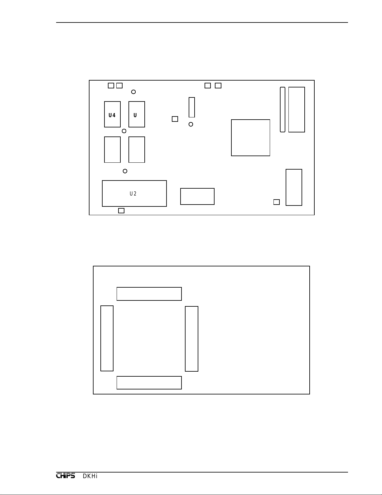
Figure 1 shows the location of the components used to configure the ABHiQV (Fab. Rev. B) daughtercard.
(front view)
(rear view)
Fi
g
ure 1: Component Location
MA0
RP1
GND3
GND4
GND2
GND1
MA1
W6
W5 W4
W3 W2
S1
W1
U8
U1
U7
U5 U6
U3 U4
U2
U4 U3
U6 U5
1
2
3
AB65555-QEDO
AB65560-SD
AB65560-QEDO
AB69000
5 DKHiQV-PCI (Fab. Rev. B) User’s Guide
&+,36
DKHiQV-PCI(Fab.Rev.B)SubjecttoChange WithoutNoticeRevision 1.3 7/2/99
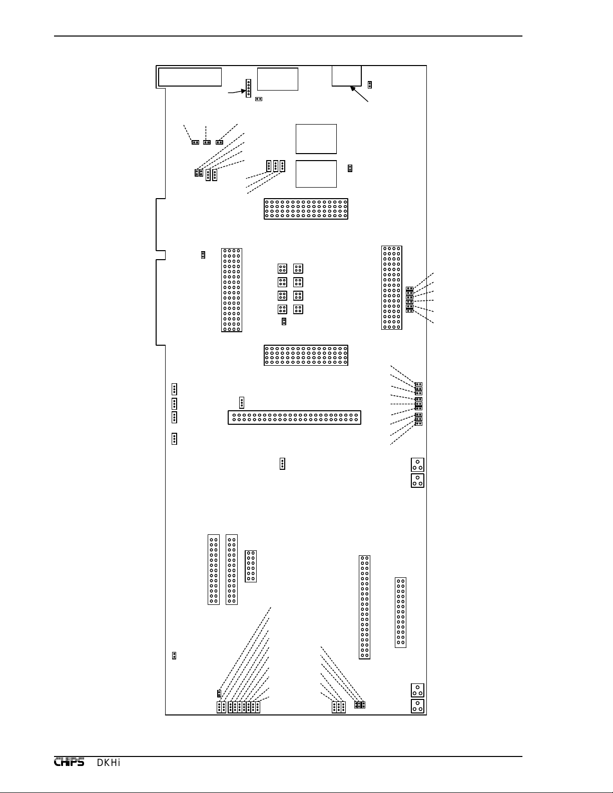
Figure 2: DKHiQV-PCI based board Jumper Location
STANDBY
J4 Video
J3 CMPS
Video
J1 S Video
W1
J2 Access Bus
JP1 JP2 JP3
W40
W8
W7
W9
W6
W5
W3
W4
JP10
JP5
JP11
JP9
JP7
JP8
JP6
JP12
JP13
W37
W36
JP4
W21
W39
W38
J5 Panel Connection
J10 J8 J9
W23
J7 MPEG Connection
J11 Panel Conn. II
R76
R75
W35
SH4
W34
W32
W33
W31
W30
W29
W28
W27
SH6
SH5
SH7
W24
W25
W26
R59
R82
W10
W12
W13
W14
W15
W16
W17
W18
W19
W20
JP19
JP15
JP16
JP18
JP20
JP17
DKHiQV-PCI (Fab. Rev. B) User’s Guide 6
&+,36
DKHiQV-PCI(Fab.Rev.B)SubjecttoChange WithoutNoticeRevision 1.3 7/2/99
4.1 Configuration Switch (S1) and Jumpers (W1 and W3)
The ABHiQV provides one on-board Dip Switch S1 and two jumpers W1 and W2 for various configuration
settings. There are three configuration bits (CFG7,4,1) which are latched from AA7,4,1 on reset. CFG7,4,1
are written into the HiQVideo controller extended register XR70[7:0].
Four additional configuration bits, CGF14:11 are latched into XR71[6:3] from MAD[6:3] on reset. The soft-
ware reserves these configuration bits for input of panel IDs. They correspond to DIP switch S1 positions
5:2 on the ABHiQV daughtercard.
All CFG pins have internal weak pull up and may be pulled down by 4.7k resistors on the daughtercard if
the DIP switches are set to ON. Table 1 summarizes all the CFG bits and corresponding DIP switches and
jumpers W1 and W3.
Refer to the applicable databook for additional configuration options.
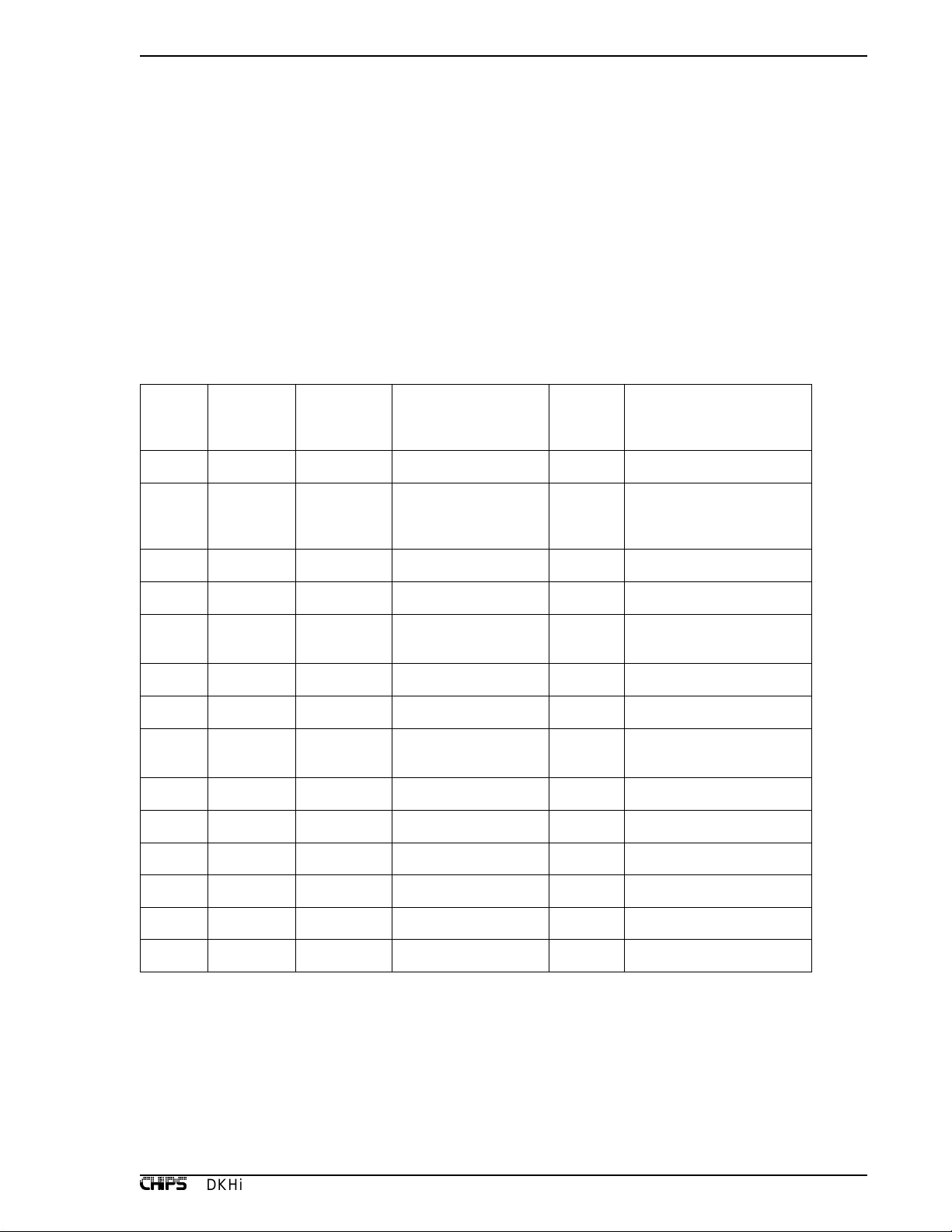
Table 1: Confi
g
uration Settin
g
s
Bits Latched
From Name Purpose XR Bits Dau
g
htercard DIP
Switch Position and
Defaults
CFG0 AA0 Reserved XR70[0]
CFG1 AA1 PCI VGA I/O Decoding
Enable/Disable on
PCI bus
XR70[1] S1[6]: open
CFG2 AA2 Reserved XR70[2]
CFG3 AA3 Reserved XR70[3]
CFG4 AA4 Ext. CLK External OSC for
MCLK and DCLK XR70[4] W1: open
CFG5 AA5 Reserved XR70[5]
CFG6 AA6 Reserved ACTI/ENABKL XR70[6] W3: open
CFG7 AA7 CLK-TST Internal clock test
mode disable XR70[7] S1[7]: open
CFG8 AA8 Reserved XR71[0]
CFG10 MA 2 Reserved XR71[2]
CFG11 MA 3 PID0 Panel Type XR71[3] S1[5]: open
CFG12 MA 4 PID1 Panel Type XR71[4] S1[4]: open
CFG13 MA 5 PID2 Panel Type XR71[5] S1[3]: open
CFG14 MA 6 PID3 Panel Type XR71[6] S1[2]: open

7 DKHiQV-PCI (Fab. Rev. B) User’s Guide
&+,36
DKHiQV-PCI(Fab.Rev.B)SubjecttoChange WithoutNoticeRevision 1.3 7/2/99
4.2 Push-on Jumpers
Table 2 lists the jumpers supported on the DKHiQV-PCI based board
Table 2: DKHiQV-PCI Jumper Descriptions
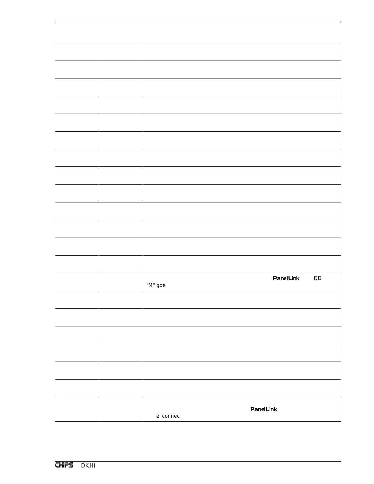
Jumper Setting Description
W1 OPEN
CLOSED Normal Mode
Standby mode
W2 OPEN
CLOSED AD722 is confi
g
ured as $FSC
AD722 is confi
g
ured as FSC
W3 OPEN
CLOSED 14 MHz oscillator enabled
14 MHz oscillator disabled
W4 1-2
2-3 External video encoder uses a dedicated 14 MHz oscillator
External video encoder shares the 14 MHz oscillator with B65555 and 69xxx
W5 OPEN
1-2
2-3
Enable TV out and disable HSYNC and VSYNC in CRT interface
Disable TV out; and enable HSYNC and VSYNC in CRT interface
ENTV controlled by SDA (GPIO 0)
W6 OPEN
CLOSED External video encoder is in NTSC mode
External video encoder is in PAL mode
W7 1-2
2-3 DDCDAT & DDCC0LK are pulled up to DVCC55X
DDCDAT & DDCC0LK are pulled up to GVCC
W8 OPEN
CLOSED External video encoder uses TSYNC (held hi
g
h)
External video encoder uses TSYNC derived from VSYNC
W9 1-2
2-3 EPROM power is from 3V main (3V)
EPROM power is from GVCC (5V)
W10 OPEN
CLOSED Combined with W11, provides card present and power requirement information
to system. See PCI spec for details.
W11 OPEN
CLOSED See description of W10
W12, 13, 14
Three 2-pin
jumpers, only
one of which
should be
closed at the
same time
-VEE uses ENAVEE (W14), ENABKL(W13) or ENAVDD (W12) as power se-
quencin
g
control
W15, 16, 17
Three 2-pin
jumpers, only
one of which
should be
closed at the
same time
VDDSAFE uses ENAVEE (W17), ENABKL(W16) or ENAVDD (W15) as power
sequencin
g
control
W18, 19, 20
Three 2-pin
jumpers, only
one of which
should be
closed at the
same time
+12VSAFE uses ENAVEE (W20),ENABKL(W19) orENAVDD (W18) as power
sequencin
g
control
W21 1-2
2-3 VEESAFE is -VEE
VEESAFE is +VEE
W23 OPEN
CLOSE U13 re
g
ulator output (3REG2) is clamped at 5V
U13 re
g
ulator output is adjustable by pot R75 (approx. 2.0-4.5V @ 1A)
DKHiQV-PCI (Fab. Rev. B) User’s Guide 8
&+,36
DKHiQV-PCI(Fab.Rev.B)SubjecttoChange WithoutNoticeRevision 1.3 7/2/99
W24 1-2
2-3 PVCC & SVCC are W25 volta
g
e
PVCC & SVCC are U13 output (see W23)
W25 1-2
2-3 W25 volta
g
e is 5VNC
W25 volta
g
e is W35 volta
g
e
W26 1-2
2-3 OSCVCC is 5V
OSCVCC is W35 volta
g
e
W27 1-2
2-3 AVCC55Xis 5VNC
AVCC55X is W35 volta
g
e
W28 1-2
2-3 IVCC55X is W29 volta
g
e
IVCC55X is output of U13
W29 1-2
2-3 W29 volta
g
e is 5VNC
W29 volta
g
e is W35 volta
g
e
W30 1-2
2-3 DVCC55X is 5VNC
DVCC55X is W35 volta
g
e
W31 1-2
2-3 MVCC55X from 5VNC
MVCC55X from 3VMAIN
W32 1-2
2-3 RAMVCC from GVCC for 5V DRAM
RAMVCC from 3VMAIN for 3V DRAM
W33 1-2
2-3 BVCC55X is +5VNC
BVCC55X is W35 volta
g
e
W34 1-2
2-3 XVCC55X is +5VNC
XVCC55X is W35 volta
g
e
W35 1-2
2-3 W35 volta
g
e is U15 output adjustable by pot R76 (approx. 2.0 - 5.5V @ 3A)
W35 volta
g
e is 3.3V from the PCI connector
W36 1-2
2-3 CVCC from 3VMAIN
CVCC from 5VNC
W37 1-2
2-3 PCLK
g
oes to panel connector J5 instead of "M" for
3DQHO/LQN
STN-DD
"M" goes to panel connector J5
W38 1-2
2-3 VDDSAFE uses GVCC (+5V)
VDDSAFE uses 3VMAIN (W35)
W39 1-2
2-3 VEESAFE is controlled by R82 (potrentiometer)
VEESAFE is controlled by W21
W40 OPEN
CLOSED 69xxx: INT# disconnected from INTA on PCI bus
69xxx: INT# connected to INTA on PCI bus
JP1 1-2
OPEN RED output has 37.5-ohm termination on-board (for TV out).
RED output has 75-ohm termination on-board (for CRT drive).
JP2 1-2
OPEN GREEN output has 37.5-ohm termination on-board (for TV out).
GREEN output has 75-ohm termination on-board (for CRT drive).
JP3 1-2
OPEN BLUE output has 37.5-ohm termination on-board (for TV out).
BLUE output has 75-ohm termination on-board (for CRT drive).
JP4 1-2
2-3
OPEN
Panel connector J5 has DVCC55X (for LVDS Interface)
Panel connector J5 has 3VREG2 (U13 for
3DQHO/LQN
Interface.
Panel connector J5 has no additional VCC
Table 2: DKHiQV-PCI Jumper Descriptions

9 DKHiQV-PCI (Fab. Rev. B) User’s Guide
&+,36
DKHiQV-PCI(Fab.Rev.B)SubjecttoChange WithoutNoticeRevision 1.3 7/2/99
Refer to schematics for additional information.
JP5
1-2
2-3
3-4
1-4
SCL for multimedia dau
g
htercard is driven by JP9 pin 3.
SDA for multimedia dau
g
htercard is driven by JP9 pin 3.
SDA for multimedia dau
g
htercard is driven by ACTI/GPIO0/CSYNC.
SCL for multimedia dau
g
htercard is driven by ACTI/GPIO0/CSYNC.
JP6
1-2
2-3
3-4
1-4
SCL for multimedia dau
g
htercard is driven by 54GPIO3.
SDA for multimedia dau
g
htercard is driven by 54GPIO3
SDA for multimedia dau
g
htercard is driven by JP9/JP10 pin 1.
SCL for multimedia dau
g
htercard is driven by JP9/JP10 pin 1.
JP7
1-2
2-3
3-4
1-4
DDCCLK for CRT is driven by 54GPIO3.
DDCDAT for CRT is driven by 54GPIO3.
DDCDAT for CRT is driven by JP9/JP10 pin 1.
DDCCLK for CRT is driven by JP9/JP10 pin 1.
JP8
1-2
2-3
3-4
1-4
DDCCLK for CRT is driven by JP9 pin 3.
DDCDAT for CRT is driven by JP9 pin 3.
DDCDAT for CRT is driven by ACTI/GPIO0/CSYNC.
DDCCLK for CRT is driven by ACTI/GPIO0/CSYNC.
JP9
1-2
2-3
3-4
1-4
JP9/JP10 pin 1 is driven by 32KHZ/GPIO1/GPIO2.
JP9 pin 3 is driven by 32KHZ/GPIO1/CSYNC
JP9 pin 3 is driven by ENABKL/GPIO1/CSYNC
JP9/JP10 pin 1 is driven by ENABKL/GPIO1/CSYNC
JP10
1-2
2-3
3-4
1-4
JP9/JP10 pin 1 is driven by 32KHZ/GPIO1/GPIO2.
32 KHz oscillator drives 32KHZ/GPIO1/GPIO2 si
g
nal
(NOT VALID)
JP9/JP10 pin 1 is driven by 54GPIO2
JP11
1-2
2-3
3-4
1-4
ENAVEE panel volta
g
e control is driven by ENABKL/GPIO1/CSYNC
ENABKL panel control is driven by ENABKL/GPIO1/CSYNC
ENABKL panel control is driven by ENAVEE/ENABKL
ENAVEE panel volta
g
e control is driven ENAVEE/ENABKL
JP12
1-2
2-3
3-4
1-4
CSYNC for TV Out is driven by ENABKL/GPIO/CSYNC.
Activity LED is driven by ENABKL/GPIO1/CSYNC.
Activity LED is driven by ACTI/GPIO0/CSYNC.
CSYNC for TV Out is drivven by ACTI/GPIO0/CSYNC.
JP13 OPEN
CLOSED CSYNC for TV out from JP11 or JP12.
CSYNC for TV out from CSYNC/HSYNC.
JP15 1-2
OPEN P34 panel data for 36-bit panels
JP16 1-2
OPEN P35 panel data for 36-bit panels
JP17 1-2
OPEN P32 panel data for 36-bit panels
JP18 1-2
OPEN P30 panel data for 36-bit panels
JP19 1-2
OPEN P33 panel data for 36-bit panels
JP20 1-2
OPEN P31 panel data for 36-bit panels
Table 2: DKHiQV-PCI Jumper Descriptions
DKHiQV-PCI (Fab. Rev. B) User’s Guide 10
&+,36
DKHiQV-PCI(Fab.Rev.B)SubjecttoChange WithoutNoticeRevision 1.3 7/2/99
5.0 Connectors
The table below identifies the function of the twelve different connectors on the DKHiQV-PCI based board.
Refer to Figure 2.
Table 3: DK Board Connector Functions
6.0 Operation
The HiQVideosingle chip LCD/CRT controllers provide a low power, high performance and minimum
component video subsystem solution. The DKHiQV-PCI evaluation board is a video adapter card that im-
plements theHiQVideocontrollers for PCI bus operation. The DK boards are very flexible and can support
the variety of high performance and low cost options supported by the HiQVideocontroller. The DK
boards support a variety of direct panel and CRT interfaces. They provide a simple and accurate way to
measure the power dissipation of various blocks of the subsystem such as the bus interface, the video mem-
ory interface and the display logic.
The DK boards have bus connectors with gold fingers which connect to the 32 bit PCI-Bus. The board pro-
vides the capability to evaluate all the following HiQVideointerfaces: bus, flat panel, CRT, memory,
MPEG, multimedia card and composite video. The boards also provide a mixed voltage capability with the
ability to measure power for different blocks of the video subsystem. The minimal component video sub-
system consists of the HiQVideochip and two blocks of DRAM (U3 and U5).
Refer to the B65555 and 69xxx HiQVideoData Books for the available resolution modes.
The user may check the power-down operation of the HiQVideocontroller using a jumper (W1) on the DK
board.
The DKHiQV-PCI based board also provides such features as:
z
Linear Acceleration
z
DC-to-DC Conversion
z
Mixed Voltage Interface
z
Power Sequencing
z
Backlight Control
6.1 Bus Interface
The DK boards interface with the standard 32-bit PCI Bus and supports burst mode operation. PCI is a local
bus interface standard widely used in the PC industry. It provides a high performance, high integration low
cost reliable and flexible solution to personal computing.
Connectors Function
J1 SVIDEO Video connector
J2 Access Bus
J3 RCA jack, composite video out
J4 15-pin VGA connector
J5 50-pin panel connector
J7 MPEG video in connector
J8, J9, J10 Multimedia card connector
J11 P30-35 Panel data for 36-bit panels
P1 PCI Bus ed
g
e connector

11 DKHiQV-PCI (Fab. Rev. B) User’s Guide
&+,36
DKHiQV-PCI(Fab.Rev.B)SubjecttoChange WithoutNoticeRevision 1.3 7/2/99
6.2 Programmable Linear Acceleration
The DKHiQV-PCI based board improves graphics performance by supporting a programmable linear ad-
dressing mode to take advantage of CHIPS 32-bit linear acceleration drivers. The programmable ’Linear
Acceleration’ video memory provides the ability to ’linearly map’ the video memory to anywhere in the 32-
bit system memory in 8MB increments, thus overcoming paging and I/O bottlenecks. High performance lin-
ear acceleration drivers are available for popular application programs such as Windows.
The user can enable or disable linearaddressing using configuration bitXR0A[1]. The user can also specify
the desired video buffer start address using PCI configuration register MBASE. When reset, the linear ad-
dressing mode is disabled and the base addresses of the video memory is at A000:0 See the PCI config-
uration section for additional information.
6.3 Memory Interface
For the B65555, the ABHiQV daughtercard is designed to support 256K x 32 EDO memory in the 100pin
PQFP mechanical package. Refer to Tables 4-1 for the resistor connections for EDO configurations.
Note: C is connected and NC is not connected.
Table 4-1: Resistor Connections for EDO Confi
g
uration
EDO
CONFIGURATION
R1 NC
R2 NC
R9 C
R14 NC
R15 NC
R16 NC
R17 NC
R18 C
R19 NC
DKHiQV-PCI (Fab. Rev. B) User’s Guide 12
&+,36
DKHiQV-PCI(Fab.Rev.B)SubjecttoChange WithoutNoticeRevision 1.3 7/2/99
The user can set the display memory type through XR41[0,1], memory size through XR42[2] and the DRAM
data bus width through XR43[4,5] for the B65555. The tables below show the possible configurations:
Note: XR41 = 01h for EDO memory, XR42 = 00h for 256-wide column and XR43 = 10h for 64-bit interface.
Table 4-2 EDO Memory Configuration Types for B65555
SIZE BANDWIDTH ORGANIZATION Qty. needed Modules
2 MB 64-bit (single bank) 256Kx32 2 U3, U5
4 MB 64-bit (dual bank) 256Kx32 4 U3, U4, U5, U6

13 DKHiQV-PCI (Fab. Rev. B) User’s Guide
&+,36
DKHiQV-PCI(Fab.Rev.B)SubjecttoChange WithoutNoticeRevision 1.3 7/2/99
6.4 Display Interface
6.4.1 Flat Panel Interface
The DKHiQV-PCI based board has a 50-pin connector (J5)which provides allnecessary signals tointerface
with any flat panel having a data word size of 24 bits or less. A second connector (J11) provides the 12
additional data bits needed for 36-bit panels. The HiQVideocontroller has enough drive for most panels
and does not require any buffering on connectors J5 and J11. Table 5 shows all the pin names for different
panel hook-ups. The HiQVideoSeries controllers provide 8mA drive on all data and control signals
(FR0A[2] must be set to 1 when DVCC = 3.3V). Figure 3 shows the pin assignments for the J5 connector.
Fi
g
ure 3: DKHiQV-PCI Flat Panel Connector Pinout
The DKHiQV-PCI based board supports simultaneous flat panel and CRT display. The HiQVideocontrol-
lers do not need an additional frame buffer for simultaneous display of CRT and single-scan flat panel dis-
plays such as TFT color panels (including 24-bit) or plasma and EL panels. For LCD-DD panels, the
HiQVideocontrollers can support simultaneous display with 60 Hz vertical refresh on both the CRT and
flat panel, or even 60 Hz vertical refresh on the CRT and 120 Hz vertical refresh on the flat panel. In this
mode, the ENAVEE(61), ENABKL (54), ACTI (53), M (69) and LP (68) pins have multiple functions. For
detailed functions, and implementations, please refer to the B65555 and 69xxx Databooks and the
DKHiQV-PCI schematics.
Name Pin # Pin # Name
[+5V] VDDSAFE 1 2 +12 VSAFE
(12 to 45V) or (-12 to -45V) VEESAFE 3 4 nc or DVCC55X (see JP4)
ENABKL 5 6 GND
M78 DE
GND 9 10 LP
FLM 11 12 GND
SNFCLK 13 14 GND
P0 15 16 P1
GND 17 18 P2
P3 19 20 GND
P4 21 22 P5
GND 23 24 P6
P7 25 26 GND
P8 27 28 P9
GND 29 30 P10
P11 31 32 GND
P12 33 34 P13
GND 35 36 P14
P15 37 38 GND
P16 39 40 P17
GND 41 42 P18
P19 43 44 GND
P20 45 46 P21
GND 47 48 P22
P23 49 50 GND

DKHiQV-PCI (Fab. Rev. B) User’s Guide 14
&+,36
DKHiQV-PCI(Fab.Rev.B)SubjecttoChange WithoutNoticeRevision 1.3 7/2/99
Pin assignments for J11 (36-bit panels) are shown in Figure 4:
Figure 4: J11 Connector Pin Assignments
6.4.2 CRT Interface
The DK Board provides direct interface to analog CRTs through an industry standard 15-pin connector (J4).
The DKHiQV-PCI based board supports non-interlaced CRT monitors with resolutions up to 1280x1024
with 16 million colors at 75 Hz. Table 5 summarizes the HiQVideopin connections for the different flat
panel configurations. Refer to the 65555 and 69xxx Databooks for the 36-pin panel support information and
pin assignments.
Name Pin # Pin # Name
GND 1 2 P24
GND 3 4 P25
GND 5 6 P26
GND 7 8 P27
GND 9 10 P28
GND 11 12 P29
GND 13 14 P30
GND 15 16 P31
GND 17 18 P32
GND 19 20 P33
GND 21 22 P34
GND 23 24 P35
GND 25 26 GND

15 DKHiQV-PCI (Fab. Rev. B) User’s Guide
&+,36
DKHiQV-PCI(Fab.Rev.B)SubjecttoChange WithoutNoticeRevision 1.3 7/2/99
Table 5: Flat Panel Connection Summary
Monochrome Color
Pin # Pin
Name DK 50pin
Connect. Single
Panel DD 8bit DD
16bit TFT
16bit TFT
18/24bit TFT HR
18/24bit STN 4bit
pack
STN
Extended
4bit Pack
STN DD
8bit STN DD
16bit
Pixels Transferred
per Shift Clock 5 1/3 2-2/3 2-2/3 5-1/3
W6 P0 15 P0 UD3 UD7 B0 B0 B00 R0... R0... UR0... UR0...
V7 P1 16 P1 UD2 UD6 B1 B1 B01 GO... B0... UG0... UG0...
Y6 P2 18 P2 UD1 UD5 B2 B2 B02 B0... G1... UB0... UB0...
W7 P3 19 P3 UD0 UD4 B3 B3 B03 R1... R2... UR1... UR1...
V8 P4 21 P4 LD3 UD3 B4 B4 B10 G1... B2... LR0... LR0...
V7 P5 22 P5 LD2 UD2 G0 B5 B11 B1... G3... LG0... LG0...
W8 P6 24 P6 LD1 UD1 G1 B6 B12 B2... R4... LB0... LB0...
U9 P7 25 P7 LD0 UD0 G2 B7 B13 G2... B4... LR1... LR1...
V9 P8 27 - - LD7 G3 G0 G00 B2... SHFCLKU - UG1...
Y9 P9 28 - - LD6 G4 G1 G01 R3... - - UB1...
V10 P10 30 - - LD5 G5 G2 G02 G3... - - UR2...
Y9 P11 31 - - LD4 R0 G3 G03 B3... - - UG2...
V10 P12 33 - - LD3 R1 G4 G10 R4... - - LG1...
W10 P13 34 - - LD2 R2 G5 G11 G4... - - LB1...
Y10 P14 36 - - LD1 R3 G6 G12 B4... - - LR2...
U10 P15 37 - - LD0 R4 G7 G13 R5... - - LG2...
U11 P16 39 - - - - R0 R00 - - - -
W11 P17 40 - - - - R1 R01 - - - -
Y11 P18 42 - - - - R2 R02 - - - -
V11 P19 43 - - - - R3 R03 - - - -
Y12 P20 45 - - - - R4 R10 - - - -
Y13 P21 46 - - - - R5 R11 - - - -
V12 P22 48 - - - - R6 R12 - - - -
U12 P23 49 - - - - R7 R13 - - - -
U6 ENABKL 5 ENABKL ENBKL ENABKLENABKL ENABKL ENABKL ENABKL ENABKL ENABKL ENABKL
Y5 SHFCLK 13 SHFCLK SHFCLK SHFCLKSHFCLK SHFCLK SHFCLK SHFCLK SHFCLK SHFCLK SHFCLK
V6M7MMMMMMMMMM
Y4 LP 10 LP LP LP LP LP LP LP LP LP LP
W5 FLM 11 FLM FLM FLM FLM FLM FLM FLM FLM FLM FLM
Y4/Y6 DE 8 DE DE DE DE DE DE DE DE DE DE
VDDSAFE 1----------
+12VSAFE 2----------
VEESAFE 42----------
GND
6,9,12,14,
17,20,23,
24,29,32,
35,38,41,
44,47,50
This manual suits for next models
1
Table of contents


