C286-LT
SERVICE
MANUAL
TABLE
OF
CONTENTS
SECTION
1
—
SPECIFICATIONS
TECHNICAL
SPECIFICATIONS.
....ueueueesesenenenenennnsnenensnnnnnnnnnenenenenne
sense
nen
1-1
SECTION
2
—
THEORY
OF
OPERATIONS
2.1
MAIN
PCB
BLOCK
DIAGRAM........ccunseneenennunsensnennensnntnnenneeneenteeteereerenn
2-1
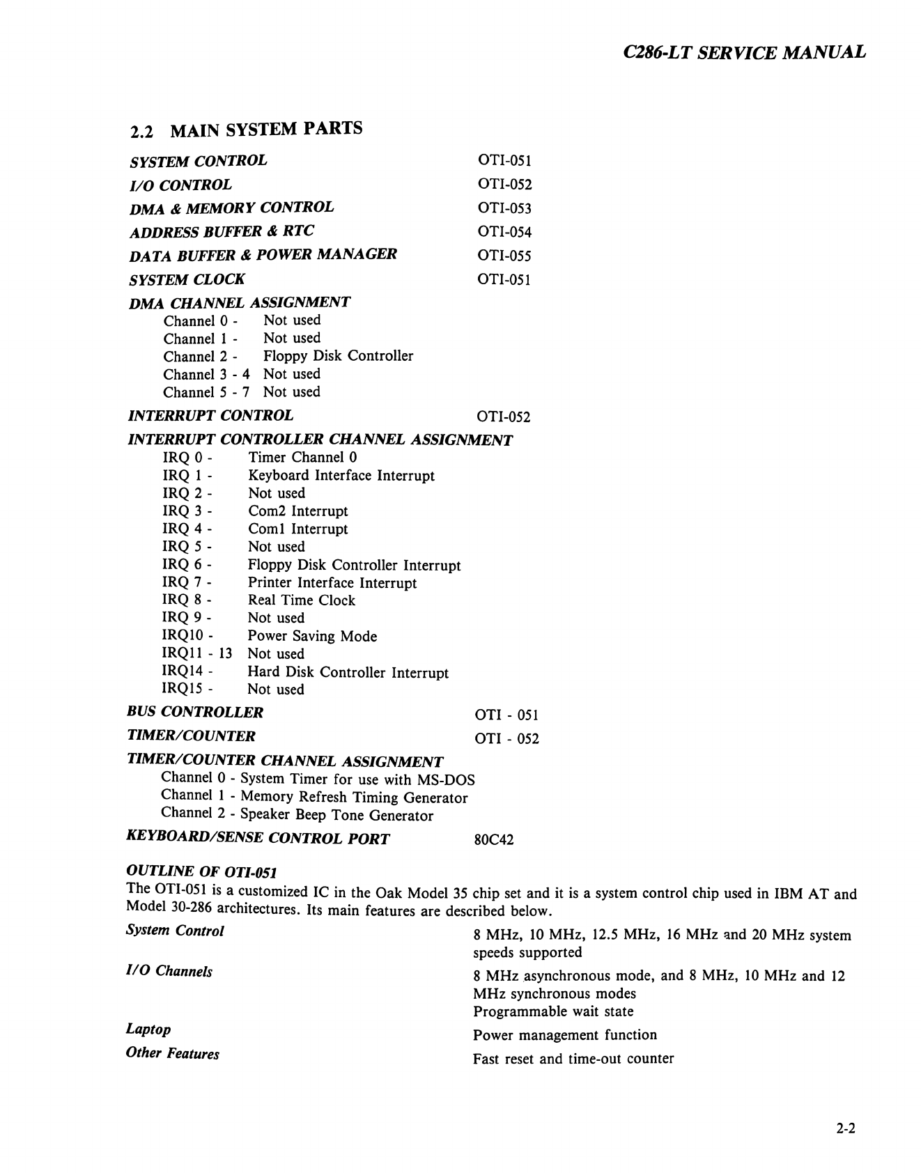
2.2
MAIN
SYSTEM
PARTS..........2222enseneensensnnsunennnunnneeennuneenneeneenteeteereeteen
2-2
2.3
SYSTEM
OVERVIEW.
.....ounnnssenseesensensunsunsnnenneneeentennenetneteeteettereeteeeeen
2-4
DD)
19
2
N
Ze
R
2-5
2.5
VGA
SYSTEM
BLOCK
DIAGRAM......uncenseesenennennsuneensenneenseeeeeeeneeereetennenn
2-6
2.6
FLOPPY
DISK
DRIVE
AND
CONTROLLER.
........cuccnneenennsunnnensunseneneneenee
nennen
2-7
2.7
HARD
DISK
DRIVE.
......2eeeneeseneeseesesunsnennunennnnensenenenenneneeneneneeeneneeenen
2-7
2.8
PARALLEL
PRINTER
INTERFACE........ceccecceneeneeneensunsnnennnennneneeneenenee
nenn
2-8
2.9
RS-232C
INTERFACE.........cccceceseeneneeeensnnunsnennenseneuneneeneeneneeneneenneeenen
2-9
2.10
MODEM
UF
SLOT.......22222eseeseseesenseseennenennennenennenneneeneneenennenennenennen
2-10
2.11
C286-LT
MEMORY
MAP.
......uceeesseeeeseesesnenesnnenenneneenenseneeneeseeenseeneeneeen
2-11
2.12
WO
ADDRESS
MAP.
.....cececeeseeeesenenseeensnennensnneesenennensenesnensenenseesenenen
2-12
SECTION
3
—
TROUBLESHOOTING
3.0
TROUBLESHOOTING
SECTION
—
CAUTION.........2ceeeeseeeneeseeeeneeseeeeeeessennenn
3-1
DISASSEMBLY
INSTRUCTIONS
FOR
C286-LT
3.1
KEYBOARD
REMOVAL
INSTRUCTIONS..........2222esseseeseeeeeeeeenseneeneneen
nennen
3-2
3.2
NICAD
BATTERY
PACK
AND
LITHIUM
CELL
REMOVAL
INSTRUCTIONS................
3-3
3.3
HDD
REMOVAL
INSTRUCTIONS........22e@seeseeeeeeseesenenesenneeneenneen
essen
nenn
3-4
3.4
LCD
POWER
UNIT
INVERTER
REMOVAL
INSTRUCTIONS...........22c2sssesseneenenen
3-5
3.5
MAIN
PCB,
POWER
SUPPLY
PCB,
FDD
AND
SPEAKER
REMOVAL
INSTRUCTIONS......
3-6
3.6
MEMORY
PCB
(OPTION)
INSTALLATION.............22cnsenseseeeeeeenesenseensennenenn
3-7
3.7
WIRING
DIAGRAM.......2cneeneeseseneseenesesneeneeseeeensenensensenessensensenennensene
3-8
3.8
TROUBLESHOOTING
ERROR
MESSAGES.
..........2.cessesseeeenseeneeeseneseee
tens
nnne
3-9
3.9
POWER
ON
DIAGNOSTICS.........2.22eeseeeeseeeeeeeeeeneeneneeeeeseneensenneren
nennen
3-10
SECTION
4
—
PARTS
COMMODORE
STOCKED
PARTS.
......ceeesseseeeeeseeeeenennneneeeennssnn
nennen
nnn
seen
4-1
SERVICE
REFERENCE
PARTS
DIAGRAM.
........cecenseeeeeenseeeeeenenesen
sense
nr
nennen
4-2
SECTION
5
—
SCHEMATICS
C286-LT
>.
|||‘
een