Crown IQ-USM 810 User manual

Digital Processor / Digital Mixer
SERVICE MANUAL
130447-1
04-00
Rev. A
©2000 by Crown International, Inc., P.O. Box 1000, Elkhart, Indiana 46515-1000 U.S.A.
Telephone: 219-294-8000. Trademark Notice: Distributed Intelligence™and IQ for Windows™
are trademarks and Crown®, IQ®, and IQ System® are registered trademarks of Crown
International, Inc. Other trademarks are the property of their respective owners.
Models:
IQ-USM 810
Some models may be exported under the name Amcron.®

IQ-USM 810 Service Manual
II
130447-1 Rev. A
©2000 Crown International, Inc.
À PRÉVENIR LE CHOC
ÉLECTRIQUE N’ENLEVEZ
PAS LES COUVERTURES.
RIEN DES PARTIES
UTILES À L’INTÉRIEUR.
DÉBRANCHER LA BORNE
AVANT D’OUVRIR LA
MODULE EN ARRIÈRE.
TO PREVENT ELECTRIC SHOCK DO
NOT REMOVE TOP OR BOTTOM
COVERS. NO USER SERVICEABLE
PARTS INSIDE. REFER SERVICING
TO QUALIFIED SERVICE
PERSONNEL. DISCONNECT
POWER CORD BEFORE REMOVING
REAR INPUT MODULE TO ACCESS
GAIN SWITCH.
CAUTION AVIS
WARNING
TO REDUCE THE RISK OF ELECTRIC
SHOCK, DO NOT EXPOSE THIS
EQUIPMENT TO RAIN OR MOISTURE!
The information furnished in this manual does not include all of the details of design, production, or variations
of the equipment. Nor does it cover every possible situation which may arise during installation, operation or
maintenance. If you need special assistance beyond the scope of this manual, please contact the Crown
Technical Support Group.
Mail: P.O. Box 1000 Elkhart IN 46515-1000
Shipping: Plant 2 SW 1718 W. Mishawaka Road Elkhart IN 46517
Phone: (800) 342-6939 / (219) 294-8200
FAX: (219) 294-8301
The lightning bolt
triangle is used to
alert the user to the
risk of electric shock.
The exclamation point
triangle is used to alert the
user to important operating
or maintenance instructions.

III
130447-1 Rev. A IQ-USM 810 Service Manual
©2000 Crown International, Inc.
Revision History
Revision Number Date Comments
Rev. A 04-2000 Initial Printing

IQ-USM 810 Service Manual
IV
130447-1 Rev. A
©2000 Crown International, Inc.
This page intentionally left blank

V
130447-1 Rev. A IQ-USM 810 Service Manual
©2000 Crown International, Inc.
Table of Contents
1 Introduction ............................................................................ 1-1
1.1 Introduction ................................................................................1-1
1.2 The IQ-USM 810 ........................................................................1-1
1.3 Warranty.....................................................................................1-1
2 Specifications ......................................................................... 2-1
3 Circuit Theory ........................................................................ 3-1
3.1 Overview ....................................................................................3-1
3.2 Power Supply .............................................................................3-1
3.3 Input ...........................................................................................3-1
3.3.1 Input Analog Processing...................................................3-1
3.3.2 Clock Signals ....................................................................3-2
3.3.3 A/D Conversion .................................................................3-2
3.3.4 DC Voltages ......................................................................3-4
3.4 Output ........................................................................................3-4
3.4.1 Clock Buffers.....................................................................3-4
3.4.2 DAC Conversion................................................................3-4
3.4.3 Output Analog Processing................................................3-4
3.5 SHARC Processing ....................................................................3-5
3.5.1 +3.3V Power Supply..........................................................3-5
3.5.2 Clocks ...............................................................................3-5
3.5.3 Reset .................................................................................3-5
3.5.4 System Control Interface...................................................3-5
3.5.5 PLDs..................................................................................3-6
3.5.6 Bus Arbitration...................................................................3-6
3.5.7 Bus Utilization....................................................................3-6
3.5.8 DSP Processing ................................................................3-6
3.5.9 Audio Routing....................................................................3-8
3.6 System Controller.......................................................................3-8
3.6.1 Control Processing............................................................3-9
3.6.2 RS232..............................................................................3-10
3.6.3 Crown Bus Loop..............................................................3-10
3.6.4 Real Time Clock ..............................................................3-10
3.6.5 Front Panel ......................................................................3-10
3.6.6 Control Port .....................................................................3-10
3.7 Front Display ............................................................................3-10
4 Maintenance........................................................................... 4-1
4.1 General Information....................................................................4-1
4.2 Definitions...................................................................................4-1
4.3 Required Test Equipment ..........................................................4-1
4.4 Message String Syntax ..............................................................4-2

IQ-USM 810 Service Manual
VI
130447-1 Rev. A
©2000 Crown International, Inc.
4.5 Standard Initial Conditions........................................................4-2
4.6 Test Procedures.........................................................................4-2
4.7 Typical Measurements...............................................................4-7
4.8 Test/Debug Objects...................................................................4-7
4.9 Display Test Patterns .................................................................4-8
4.10 Error Codes..............................................................................4-9
4.11 Troubleshooting FAQs .............................................................4-9
5 Parts Information................................................................... 5-1
5.1 General Information ..................................................................5-1
5.2 Ordering and Receiving Parts ..................................................5-1
5.2.1 Terms .....................................................................................5-1
5.2.2 Shipment ................................................................................5-1
6 Exploded View Parts ............................................................. 6 -1
7 Module and Schematic Information..................................... 7 -1
8 Module Parts.......................................................................... 8-1
PWA 126451-3 .................................................................................8-3
PWA 126690-3 ...............................................................................8-13
PWA 126693-4 ...............................................................................8-47
PWA 126744-3 ...............................................................................8-59
PWA 128045-1 ...............................................................................8-65
PWA 128047-3 ...............................................................................8-75
PWA 128047-4 ...............................................................................8-87
PWA 128049-1 ...............................................................................8-99
PWA 128051-3 .............................................................................8-117
9 Schematics ............................................................................ 9-1
Table of Contents

Introduction1-1
130447-1Rev.A IQ-USM 810ServiceManual
©2000 Crown International, Inc.
1.1 Introduction
This manual contains complete service information
on the Crown®IQ-USM 810 Digital Processor/Digital
Mixer. It is designed to be used in conjunction with
the Reference Manual; however, some important in-
formation is duplicated in this Service Manual in case
the Reference Manual is not readily available.
NOTE: THE INFORMATION IN THIS MANUAL IS
INTENDEDFORUSEBYAN EXPERIENCEDTECH-
NICIAN ONLY!
1.2 The IQ-USM 810
The Crown IQ-USM 810 is an 8x10 mixer/processor
that provides unique dual input processing paths. As
an IQ®component, it can be controlled by an IQ Sys-
tem®, and with its distributed intelligence™capability,
continue to operate even when an IQ System is not
connected. The IQ-USM 810 can also act as a sys-
tem interface to other IQ components.
The IQ-USM 810 features high-quality 24-bit A/D and
D/A converters along with 240MIPS of full 32-bit float-
ing point DSP for optimum dynamic range.
Thedualinput processingpathsinclude a full comple-
ment of signal processing features, including ad-
vanced algorithms for gating, auto-leveling, filtering,
compression and automixing.
A full 8x8 Matrix Mixer allows any combination of rout-
ing and mixing from any input to any output. The Ma-
trix Mixer outputs are routed to the two Main Audio
Outputs and eight AUX Audio Outputs. The Main and
AUX Audio Output sections further process the sig-
nal with individually adjustable signal delay and fil-
ters along with an Ambient-Leveler and a high perfor-
mance Output Limiter for system protection.
A Multi-Function Control Port implements analog and
digital I/O for control and monitor by simple potenti-
ometer and switch wall controllers and indicator pan-
els.
All of the IQ-USM 810 parameters are backed up via
reliable FLASH memory. System configurations may
be stored for recall from any of thirty-two system pre-
sets from the front panel control or via IQ for Windows
software.
1.3 Warranty
Each Reference Manual contains basic policies as
relatedtothecustomer. In addition,itshould be stated
that this service documentation is meant to be used
only by properly trained personnel. Because most
Crown products carry a 3-Year Full Warranty (includ-
ing round trip shipping within the United States), all
warrantyservice should bereferredto the CrownFac-
tory or Authorized Warranty Service Center. See the
applicable Reference Manual for warranty details. To
find the location of the nearest Authorized Warranty
Service Center or to obtain instructions for receiving
Crown Factory Service, please contact the Crown
Technical Support Group (within North America), or
yourCrown/AmcronImporter(outsideNorth America).
If you are an Authorized Warranty Service Center and
have questions regarding the warranty of a product,
please contact the Crown Factory Service Manager
or the Crown Technical Support Group.
1 Introduction
Crown Customer Service
Technical Support Group
Factory Service
Parts Department
Mailing Address: P.O. Box 1000, Elkhart IN 46515
Shipping Address: Plant 2 S. W.
1718 W. Mishawaka Rd., Elkhart IN 46517
Phone: (219) 294-8200
Toll Free: (800) 342-6939
Fax: (219) 294-8301
http://www.crownaudio.com

IQ-USM810ServiceManual
1-2Introduction
130447-1Rev.A
©2000 Crown International, Inc.
Figure 1.1 IQ-USM 810 Front and Rear Views

Specifications 2-1
130447-1 Rev. A IQ-USM 810 Service Manual
©2000 Crown International, Inc.
2 Specifications
General
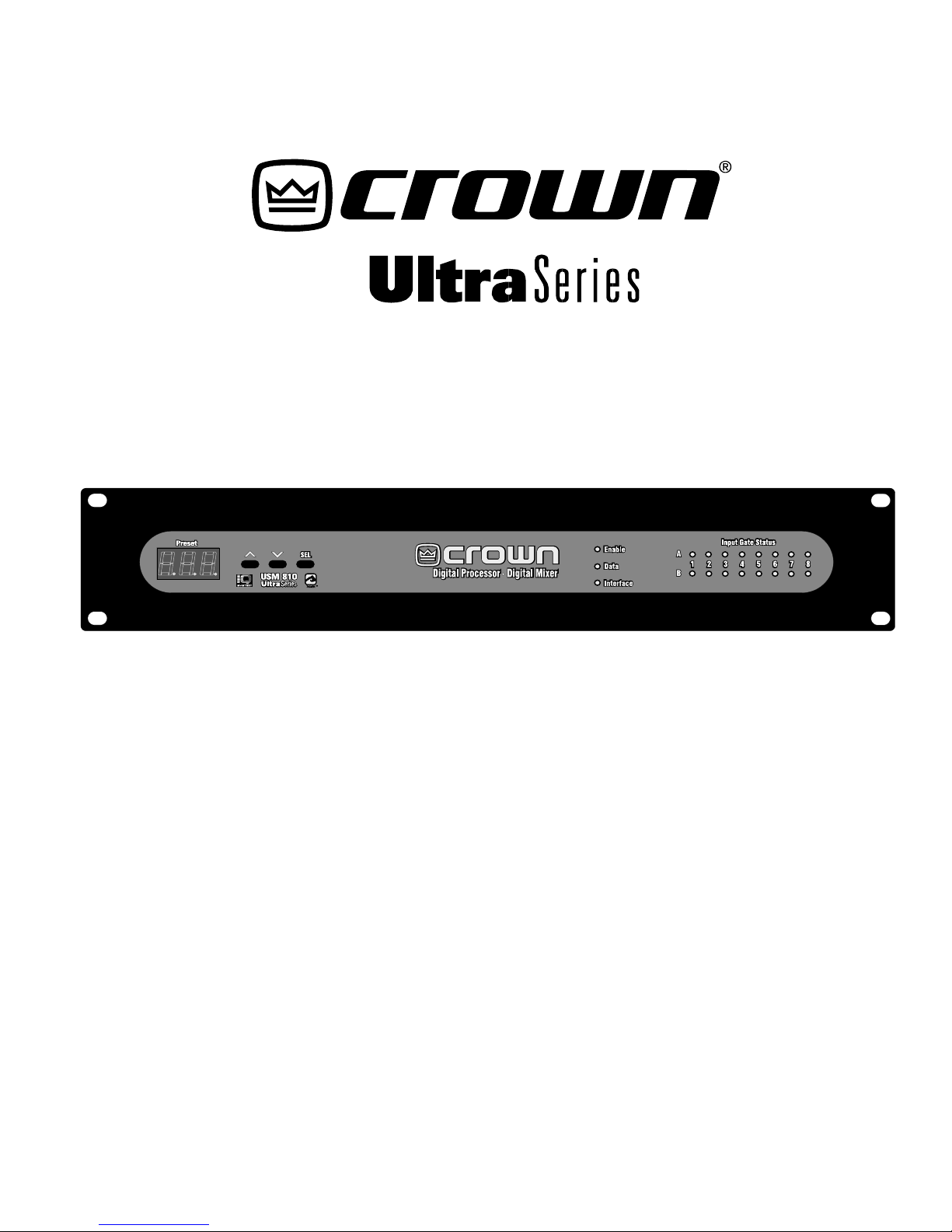
Front Panel Controls: Front-panel switches select IQ
Address, Baud Rate, factory default preset (P00), and
any of 32 user-defined presets (P01–P32).
Rear-Panel Controls: A 3-position selector switch
(mic/line/phantom) and a calibrated gain control for
each input.
Connectors: Crown Bus: RJ-45 for input/output, RJ-45
for daisy output, RS232: DB9F computer interface for
both component and interface modes. Multi-function
Port: DB37M for analog inputs, digital inputs, digital
outputs, +5VDC, +10VDC and Ground. Audio Inputs
and Outputs: 3-pin male removable barrier block con-
nectors, Euro-style cable connector supplied. AC
Power: IEC320 connector for AC power cord.
Display:A blue front-panel Enable indicator lights to
show that the unit is plugged in and AC power is being
supplied. An amber front-panel Data Signal Presence
Indicator (DATA) flashes whenever commands ad-
dressed to the IQ-USM 810 are received. A green
front-panel Interface indicator lights when the IQ-USM
810 is being used as system interface. A three-digit
digital display indicates the IQ-USM 810’s initialization
sequence by displaying each processor’s name as it
comes online, indicates the presently selected preset,
indicates the IQ address and baud rate while those
parameters are being adjusted, indicates when a pa-
rameter has been stored in flash memory, and when
any parameter is varied from its value within the cur-
rently selected preset. Ladder Display: A front panel,
sixteen-segment LED display matrix can be set to
three different operating modes: Level Meter, Input
Gate Status, and Infinity Pattern.
Power Requirements: 100VAC to 240VAC, 35VA
nominal.
Protection: if communication is lost, the unit will con-
tinue to function with the last commands received.
RS232 Data Communication
Baud Rate: Selectable to 19.2 K, 38.4 K, 57.6 K, or
115.2 K BAUD.
Data Format: Serial, binary, asynchronous; 1 start bit;
1 stop bit; 8 data bits; no parity.
Crown Bus Data Communication
Data Rate: 38.4 K BAUD.
Data Format: Serial, binary, asynchronous; 1 start bit;
1 stop bit; 8 data bits; no parity.
Crown Bus Interface Type: Optically isolated 20 mA
current loop.
Operation: Half-duplex.
Transmission Distance: Variable from 200 to 3000
feet (61 to 914 meters), depending upon wire capaci-
tance. Typically 1000 feet (305 meters) using shielded
twisted-pair wire, #26 AWG or larger. Can be extended
with an IQ Repeater.
Audio
PhantomVoltage: +24VDC at 10 mA.
Input Gain Range: +20 dB to –12 dB.
Digital Sampling: 24 bit, 48 kHz.
Input Impedance: 20 k ohms balanced, 10 k ohms
unbalanced.
Dynamic Range: Greater than 100 dB (A-weighted,
20 Hz–20 KHz).
Frequency Response: ± 0.5 dB, 20 Hz–20 kHz.
Common Mode Rejection: 50 dB (typical).
Crosstalk: Greater than 80 dB at 10 kHz.
Total Harmonic Distortion: Less than 0.05% THD + N
(1 kHz, 0 dBu).
Output Impedance: 100 ohms balanced, 50 ohms
unbalanced.
Max Input Level: +32 dBu (line) or +7 dBu (mic).
Max Output Level: +20 dBu.
Control Port
Power Supply: +5VDC and +10VDC outputs are pro-
vided. The total output current is limited to 1A.
Outputs
Logic Low: less than 0.1V.
Logic High: 10V (via internal pull-up).
Output Current is limited to 10mA max per pin.
Inputs
Input Impedance: greater than 50 k ohms.
Logic Low: less than 0.5V.
Logic High: greater than 5V.
Analog Range: 0 to 10V (for inputs 9-16 only).
Max InputVoltage: 25V.
Mechanical
Weight: 13 pounds, 4 ounces (6.1 kg).
Dimensions: 19-inch (483-cm) standard rack mount
width (EIA RS-310-B), 16-inch (40.6-cm) depth behind
mounting surface, and 3.5-inches (8.9-cm) height.

IQ-USM 810 Service Manual
2-2 Specifications
130447-1 Rev. A
©2000 Crown International, Inc.
This page intentionally left blank

©2000 Crown International, Inc. Circuit Theory 3-1
130447-1 Rev. A IQ-USM 810 Service Manual
3 Circuit Theory
3.1 Overview
This section explains operation of the IQ-USM 810 cir-
cuitry.PleaserefertotheIQ-USM810ReferenceManual
and IQ for Windows help files for information about the
IQ-USM 810 features and operation.
The IQ-USM 810 consists of a universal power supply
and 5 PWAs (see Figure 3.1). Each PWA has a particu-
lar function and initial troubleshooting should focus on
attemptingtodeterminewhichPWAiscausingthemal-
function.ThePWAsarenotunit-dependent, so aknown
goodworkingPWAorunitcanbeusedtopinpointwhich
PWA is faulty.
3.2 Power Supply
The universal power supply used by the IQ-USM 810
resides underneath the System Controller at the back
of the unit. It receives AC input from the IEC filter lo-
cated on the back panel and supplies +15V, –15V, and
+5VDCtotheSystemController. Thereisafuselocated
onthe supplyand shouldbe checkedif thepower sup-
ply is suspected. Replace fuse with the same rated
typeonly.
3.3 Input
The input Printed Wire Assembly (PWA) is located at
the back of the unit on the bottom. It offers eight bal-
anced input audio channels via 3 pin connectors. Fig-
ure 3.2 shows the block diagram of the input PWA. The
PWA is composed of the following sections: Input Ana-
logProcessing,ClockSignals,A/DConversion,andDC
Voltages.
3.3.1 Input Analog Processing
Each input channel has analog processing that pro-
vides filtering, line/mic switching, phantom power, op-
tionalinputtransformerisolation,andvariablegaincon-
trol.Thebalanced output ofeach analogchannel isfed
to a shared A/D converter.
Alleightanaloginputchannelsareidentical(Figure3.3).
The balanced analog input is RF filtered by FB100,
FB101, C102, and C103. Capacitors C100 and C101
provide filtering to ensure that no noise from the unit
goesout. R100-102providea 10 k ohm balanced input
impedance in the line mode. Switch SW100 provides
switching between Phantom, Line, and Mic modes.
• Phantom: SW100 shorts R103/C104 and R104/
C105 to allow the phantom DC voltage (+24VDC)
to be available on the input connector. In addi-
tion, no gain reduction is provided on the input
path. R105 & R106 allows current limiting of the
phantom voltage.
Figure 3.1 Overall Block Diagram

©2000 Crown International, Inc.
IQ-USM 810 Service Manual
3-2 Circuit Theory
130447-1 Rev. A
• Line: In Line mode, both the coupling capacitors
(C104 & C105) and the series resistors (R103 &
R104) are in the signal path. The capacitors block
the phantom voltage from the input while the se-
ries resistors work as a voltage divider with R105
& R106 to provide a 17.7x (25 db) reduction in
gain.
•Mic:Thecouplingcapacitorsareprovidedtoblock
the phantom power, but the series resistors are
shorted, allowing full gain through the input chan-
nel.
L100/C106(L101/C107)provideanadditionallow-pass
filter. C108 & C109 provide coupling to the variable
gain preamp, except when the optional input isolation
transformer (T100) is in place. Q100 and Q101 form a
differential amplifier whose gain is adjusted by R111.
U100B provides a filtered differential to single-ended
conversion. U101C provides a gain reduction and bi-
ases the input signal to +2.2VDC. The output bias volt-
ageoftheA/Dconverter'spin15isfedtotheopampto
bias the signal to the A/D's bias point. Lack of voltage
at pin15 is an indication that the A/D converter is either
in reset or is not being clocked.
3.3.2 Clock Signals
The master oscillator for the audio signals is Y1, which
generates a 12.288 MHz signal (256Fs). This clock is
buffered by U3 and provides separate outputs to each
of the A/D converters, the Output PWA for the DAC's,
and to the SHARC PWA for distribution to the optional
CobraNet™ (CNET) PWA.
U1 normally acts as the generator of the Serial Clock
and the Frame Clock. Serial Clock provides the timing
of the serial audio data, 3.032 MHz (64Fs), and Frame
Clock is the actual sampling clock frequency, 48 kHz
(Fs). U1 monitors the CNET line from the SHARC PWA
immediately out of reset. If the pin is low, it acts as a
master source and begins providing Serial Clock and
FrameClocktoU4& U5 for bufferingand distribution. If
U1 senses a high on the CNET pin out of reset, it oper-
ates in slave mode like the other A/D converters and
waits for Serial and Frame Clocks from the CNET PWA.
3.3.3 A/D Conversion
Each A/D converter processes 2 input channels. Full
scale input signals are 2.82Vp-p and are sampled at a
48-kHz rate with 24-bit resolution. The converters are
reset by the DSP's by the IO_RST line with a low being
reset.The convertersprovideanI2S32-bit time-division
multiplexed data audio stream. The most significant 24
bits are linear PCM (two's complement) audio data fol-
lowed by 8 bits of converter peak hold data that is un-
Figure 3.2 Input PWA Block Diagram

©2000 Crown International, Inc. Circuit Theory 3-3
130447-1 Rev. A IQ-USM 810 Service Manual
Figure 3.3 Input Analog Processing Circuitry (one channel)

©2000 Crown International, Inc.
IQ-USM 810 Service Manual
3-4 Circuit Theory
130447-1 Rev. A
Each DAC takes a 2 channel I2S 32-bit time-division
multiplexed data audio stream from the SHARC PWA
andconverts it at a 24-bit,48-kHzrate(Figure3.4).Like
the A/D converter, the audio output of the DAC is bi-
ased positive by 2.2V and a full signal is 2.82Vp-p.
3.4.3 Output Analog Processing
Alltenanalogoutputchannelsareidentical(Figure3.6).
The balanced output of the DAC drives a unity gain
amplifier that also filters the audio signal. The single-
ended output is fed to U101A which provides gain of
either 1.2 (+10 dbu) or 3.9 (+20 dbu). Z100 is normally
open, which provides a +20 dbu output for a full scale
signal from the DAC. U101C provides a gain reduction
of 2, then U101D inverts the signal and provides the
otherbalancedoutput.Anoutputimpedanceof50ohms
is provided by the series resistors while the output fer-
rite bead provides RF filtering to ensure isolation. Op-
tional isolation transformers are available on the Main
outputs by removing the series resistors and placing
the transformers.
Figure 3.5 Output PWA Block Diagram
used. This data is routed to the SHARC PWA for pro-
cessing(ADC1-4).Figure3.4showstheaudiodataand
its relationship to the clock signals.
3.3.4 DC Voltages
The Input PWA receives +/–15V and +5V from the Sys-
temController.+15VfromP900 isfilteredandthenregu-
lated by a low dropout regulator, U900. R900 & R901
set the output voltage of the regulator at +14.5V. The
–15VisprocessedsimilarlybyU901.The+5Visfiltered
separately for the digital portion of the PWA than the
analog side.
ThephantompowervoltageisgeneratedbyU902.+15V
from P900 drives L904 while Q900 acts as a switch to
charge L904. R905 acts as a current sense and limits
the output current of the phantom power by reducing
the voltage at currents over 50 mA. R904 & R908 set
the output voltage at about +26V. U902 is driven from a
96-kHz clock provided by U10. This ensures that the
switching supply is synced to the sampling frequency
of the converters (2Fs). During reset, U902 will run at a
slightlylowerfrequencyduetothelackofaninputclock.
3.4 Output
The Output PWA sits on top of the Input
PWAandprovides10audiooutputs;Main
A/B and AUX 1-8. The Output PWA re-
ceivesallofitssignals fromtheInputPWA
via a 26-pin ribbon cable. Functionality
can be divided into Clock Buffers, DAC
Conversion, and Output Analog Process-
ing. A block diagram of the Output PWA
is shown in Figure 3.5.
3.4.1 Clock Buffers
Threeclockbuffers,U1-3,accepttheMas-
ter(12.288MHz),Serial(3.032MHz),and
Frame(48kHz)clocksfromtheInputPWA
and provide separate outputs to each of
the five DAC's.
3.4.2 DAC Conversion
Figure 3.4 Audio Data and Clock Signals

©2000 Crown International, Inc. Circuit Theory 3-5
130447-1 Rev. A IQ-USM 810 Service Manual
3.5 SHARC Processing
TheSHARC PWAsitsin thecenter ofthe chassisand is
the DSP engine that provides all of the signal process-
ing for the unit. At the core of this processing is four
Analog Devices ADSP-21065L SHARC 32-bit floating
point DSP's running at an internal rate of 60 MHz. Full
speed SDRAM interface is provided. Figure 3.8 shows
theblockdiagram oftheSHARCPWA.Featuresinclude
a +3.3V Power Supply, Clocks, Reset, System Control-
lerInterface,PLD's,BusArbitration,BusUtilization,DSP
Processing, and Audio Routing.
3.5.1 +3.3V Power Supply
TheentireSHARCPWAutilizes+3.3Vbytakingthe+5V
fromP1andconvertsitto+3.3Vusinga300-kHzswitch-
ing supply IC, U29. Q2 & Q3 work with U29 to control
the charging of L1. R200 current senses the supply for
overload protection. C27 & C113 provide output filter-
ing of the supply.
3.5.2Clocks
Oscillator Y1 provides a 30-MHz clock to buffer U3 for
distribution to all SHARC's, SRAM, and other circuitry.
3.5.3 Reset
U8 monitors both the +5V and +3.3V power supplies
and places the SHARC's into reset if either supply
droops. In addition, the System Controller uses U8 to
reset the SHARC's using pulldown via D1. Switch S1
allows manual reset of the SHARC's for troubleshoot-
ing.Q1monitorstheresetlinetotheSHARC'sandlights
LED E5 when the SHARC's are not in reset. The active
low \RST line resets all four SHARC's and the PLD's
(U9, U11, U23, U24, and U30).
3.5.4 System Controller Interface
Communications between the System Controller and
SHARC processors occurs through a series of latches
(U12-22) that provide address and data. PLD U23 re-
ceives commands from the System Controller (SH_A0-
2, \HCS, HR/W) to load data and addresses into these
latches. Once the data is in the latches, U23 communi-
cateswithArbiterPLDU24(\SYSBR,\SYSBG,\RD,\WR)
to request access to the SHARC bus.
There are no non-volatile memory resources on the
SHARC PWA, so the System Controller stores the
SHARC firmware and downloads it during boot. The
SystemControllerbootseachSHARCinsuccession by
loading code into SRAM and into each SHARC via the
Interface. OnceallfourSHARChavebeenbooted,they
are allowed to begin audio processing.
If the System Controller encounters any problems dur-
ing the boot process, it will display an error code on the
front panel display. These error codes are shown in the
table in Figure 3.7:
Figure 3.6 Output Analog Processing Circuitry (one channel)
Note: Errors 1-9 are for power-up self test and other
miscellaneous errors. Errors 10-25 are errors related to
the SHARC subsystem.
Figure 3.7 System Controller Error Codes
E1 UART failed system controller power-on self test
E2 RAM failed system controller power-on self test
E3 Application code in flash failed CRC test
E4 Flash verify error
E5 Unrecoverable firmware error
E10 SHARC 0 interface hardware error (timeout, etc.)
E11 SHARC 1 interface hardware error (timeout, etc.)
E12 SHARC 2 interface hardware error (timeout, etc.)
E13 SHARC 3 interface hardware error (timeout, etc.)
E22 SHARC 0 software watchdog timeout
E23 SHARC 1 software watchdog timeout
E24 SHARC 2 software watchdog timeout
E25 SHARC 3 software watchdog timeout

©2000 Crown International, Inc.
IQ-USM 810 Service Manual
3-6 Circuit Theory
130447-1 Rev. A
Figure 3.8 SHARC PWA Block Diagram
The System Controller will display the error code, then
begin the boot process again. By watching the boot
processon the frontdisplay,theerrorcode can beread
at the end of the boot process before the next boot be-
gins.
3.5.5 PLDs
There are five Programmable Logic Devices (PLD) on
the SHARC PWA (U9, U11, U23, U24, and U30). These
IC's are programmed on the PWA and can be repro-
grammed. They have common control and clock lines
(ETCK, ETMS) and are daisy-chained by having each
output (TDO) tied to the next PLD's input (TDI). P3 al-
lows connection to the external PLD programmer.
3.5.6 Bus Arbitration
The32-bitdataand24-bitaddressbussesoftheSHARC
PWA are shared between the System Controller and
the four SHARC processors. Shared SRAM memory
(U5-6) is also available to all processors. The Arbiter
PLD,U24,policeswhichhas access to the busthrough
the use of control signals such as bus requests (\HBR,
\SYSBR, \BR0-3), bus grants (\HBG, \SYSBG, \BG0-3),
and SHARC chip selects (\CS0-3). It regulates which
and when each processor has control of the bus to en-
sure there is no contention.
3.5.7 Bus Utilization
TheArbiterPLDalsoworks with theBusUtilizationPLD,
U30,tomonitor each SHARCprocessoranddetermine
howmuchofthe availableSHARCbusbandwidtheach
is using. The Arbiter tells the Utilization PLD on an indi-
vidualbuscycle basis wheneach SHARC isonthe bus
(UTILIN0-5) and this information is fed to the individual
SHARC's pulse width modulation inputs (UTILOUT0-3)
for calculation of bus access time. This information is
thenreportedtothe System Controllerwhenrequested.
3.5.8 DSP Processing
Asstated,thefourSHARCprocessors(U25-28)arethe
core of the DSP engine. These processors are 208-pin
PlasticQuadFlatPacks(PQFP)andthepinoutisshown
in Figure 3.9.
Each SHARC has a specific task in the audio process-
ing chain. SHARC 0 (U25) processes the input audio
for channels 1-4, while SHARC 1 (U27) is tasked with
the input audio processing for channels 5-8. Two chan-
nel serial audio data from the Input Router, U9, is sent
totheappropriateSHARC'sserialportalongwithaudio
clocksignalsSerialClock(SCK)andFrame Clock (FS).
TheinputaudioisstoredbytheSHARCuntil16samples
are accumulated, then this audio “brick” is processed.

©2000 Crown International, Inc. Circuit Theory 3-7
130447-1 Rev. A IQ-USM 810 Service Manual
The time allotted for the SHARC to process this audio
data is 330us (16 samples x 48-kHz). At that point the
next audio brick has been collected and is ready for
processing. The processed output audio brick is then
deposited into SRAM (U5, U6). The audio bricks are
then taken by the Output SHARC's for mixing and out-
putprocessing. SHARC2(U26)processesMainAand
Outputs 1-4 while SHARC 3 (U28) is responsible for
Main B and Outputs 5-8. If additional delay is required,
the bricks are allowed to remain in SDRAM before pro-
cessing.Theminimumdelaythroughtheaudioprocess-
ing is as follows:
• A/D Conversion 667us
• 5x "brick" delay 1667us
• DAC Conversion 520us
• Total Delay 2854us
This delay is constant and not dependent upon the
particular processing being done.
SDRAM provides a high speed synchronous memory
resource. Only the four SHARC processors have ac-
cess to SDRAM and they are responsible for the ac-
cess and maintenance of it. Each SHARC monitors the
Figure 3.9 SHARC Pinout

©2000 Crown International, Inc.
IQ-USM 810 Service Manual
3-8 Circuit Theory
130447-1 Rev. A
bus and accesses SDRAM when it is available. The
SHARC blocks access to the bus through the use of
the \SDLOCK pin during SDRAM transfers. SDRAM is
utilizedonlyforaudiodelayprocessingandhasnofirm-
ware. If audio is available at the input SHARC's, but is
notbeingseenbytheoutputSHARC's,a good place to
begin troubleshooting would be with SDRAM.
The System Controller periodically accesses the
SHARC'sto query about meter data. As discussed, the
System Controller utilizes the Interface to ask and re-
ceive this data.
3.5.9 Audio Routing
Serial audio from the Input PWA is sent to the SHARC
PWA for processing. ADC1-4 is fed to PLD U9 for rout-
ing to the input SHARC's, U25 & U27. Serial digital au-
dio from the optional CobraNet PWA is also available
as CNET_TX1-4. The Input Router sends the appropri-
ate serial audio data to the input SHARC's as directed
by the System Controller via SHARC 1. A serial control
link (IN_MOSI, IN_SPICK) tells the Input Router which
oftheserialdigitalinputsaretobesenttoeachSHARC's
serial ports.
The Input Router is also responsible for buffering the
audioclocks.By sensingtheCNETinputfromtheCNET
PWA, the Input Router can tell if the CNET PWA is con-
nected. If CNET is available, the CNET PWA is respon-
sible to provide the Serial and Frame Clocks. The PLD
accepts the CNET audio clocks and routes them to the
SHARC's and Input PWA. If the CNET PWA is not con-
nected, the audio clocks from the Input PWA are ac-
cepted and routed to the SHARC's.
The Output Router, U11, is responsible for sending the
serial audio outputs of the output SHARC's to the ap-
propriate place. Five output lines, DAC1-5, allow 10
audio channels to be sent to the Output PWA for DAC
conversion.In addition, fouroutput lines, CNET_RX1-4,
allow 8 audio channels to be directed to the optional
CNET PWA for inclusion onto the CNET system. The
Output Router is programmed by SHARC 2 via
OUT_MOSI & OUT_SPICK.
3.6 System Controller
The System Controller PWA sits on the one side of the
chassis and is supported over the power supply. It is
responsibleforthecoordinationandcommunicationwith
the outside world, non-volatile memory storage of all
code, and various other functions. The System
Controller's tasks includes Control Processing, RS232,
Crown Bus loop, Real-Time Clock, Front Panel, and
Control Port. Figure 3.10 shows a block diagram for the
System Controller PWA.
Figure 3.10 System Controller Block Diagram

©2000 Crown International, Inc. Circuit Theory 3-9
130447-1 Rev. A IQ-USM 810 Service Manual
3.6.1 Control Processing
The brain of the System Controller PWA is the Motorola
68HC12 microcontroller, U15. The 112pin QFP pinout
is shown in Figure 3.11.
TheHC12hasa BackgroundDebug Mode (BDM)con-
nection that allows access to the internal workings of
themicrocontroller.ByconnectingapodtoP9andplac-
ingtheHC12inBDMmode,theHC12canbeaccessed.
This function is not used in normal operation or trouble-
shooting, and the BDM jumper should be left in the
NORM position.
The HC12 provides all of the processing for the control
of the IQ-USM 810. U16 provides sensing of the +5V
power supply and brings the HC12 out of reset once
the supply is stable. Switch S1 allows resetting of the
controllerexternally.Q17monitorstheresetlineandLED
E1 is lit whenever the processor is not in reset.
Crystal Y2 provides the 14.7456-MHz clock for the
HC12. The clock is buffered by U5D and is provided to
dual UART U2 for baud rate creation.
When the HC12 comes out of reset, it looks to the flash
memory (U13) and begins its boot process. Due to the
slow response of flash memory, normal code process-
ing is carried out in SRAM. The HC12 copies its firm-
ware out of flash memory into SRAM (U14) and once
complete, jumps to SRAM and begins code process-
ing. The HC12 initializes the dual UART and looks for a
break on the RS232 input. If a break is detected, it acti-
vates its loader routine and waits for 'S' records from
theRS232porttobedownloadedtoflash memory.This
process allows external programming of firmware revi-
sions.
If no break is detected, the HC12 begins loading the
SHARC firmware from flash memory into SHARC
memory via theSystem ControllerInterface. U8 andU9
provide buffering to the SHARC PWA via P1.
Figure 3.11 68HC12 microcontroller Pinout

©2000 Crown International, Inc.
IQ-USM 810 Service Manual
3-10 Circuit Theory
130447-1 Rev. A
The HC12 firmware uses a real time operating system
(RTOS) to make efficient use of the HC12's processing
capability. Various tasks are given priorities, and the
RTOS supervises what task has control of the proces-
sor at any particular time.
3.6.2 RS232
As mentioned, the RS232 port is used to load firmware
into flash memory. UART U2 provides the serial port
interface to the HC12. The baud rate is programmed
by the HC12 as directed by the front panel (19.2 k to
115 kbps) and the clock is generated from the 14-MHz
clock. The 8-bit parallel interface to the UART is con-
trolled by the U_RD (read), U_CS (chip select), and
FLSH_WE (write) lines. Internal registers control vari-
ous functions such as baud rate, fifo usage, etc. The
serialI/OoftheUARTisbufferedbyRS232Tx/Rxdriver
U1. This buffer takes the +5V and creates the +/–12V
needed for RS232 levels. These signals are available
on the DB9F connector, J1, which is available on the
back panel of the chassis.
The other half of dual UART U2 is used as a serial inter-
facetotheoptional CNETPWA.ItconnectstotheCNET
PWA via SHARC connector P1.
3.6.3 Crown Bus Loop
The HC12 has two serial ports and one of them is used
for the interface to the Crown Bus loop hardware. This
is a fixed 38.4-kbps baud rate and uses a dual RJ45
connector J2 to the back panel. In normal operation,
data detected at the input of the Crown Bus loop hard-
ware is sent back out via U19A & B, U20B, and U21A.
WhentheHC12wantstocommunicate,MSTR0ispulled
highand the TX0goes out tothe CrownBus loop. R142
provides 20 mA of current to the OUT+ line during nor-
mal operation. Communication occurs by interrupting
the OUT– path via D4 and U21A.
The input of the Crown Bus loop is buffered by
optoisolator U17 which senses the 20-mA current and
sendsthesignals to theHC12(RX0) and directsit back
out the Crown Bus loop via U19A.
Relay K1 provides paths to the I/O circuitry while the
IQ-USM810ispowered.Whentheunitisturnedoff,the
relay allows the Crown Bus loop to pass through the
unit to prevent Crown Bus loop communication from
being interrupted.
3.6.4 Real Time Clock
U11 is a Real Time Clock (RTC) IC that provides timing
to the HC12 for scheduling of real time events. U11 has
aninternaloscillatorprovidedby32-kHzcrystalY1.The
HC12 communicates with the RTC via a serial interface
composed of RTCLK (serial clk), RTC (data), and
RTC_CS (chip select) and periodically queries the RTC
to get or set the time.
Capacitor C25 is a 1F supercap that allows the RTC to
continue to keep time after the unit is powered down.
The RTC senses the loss of power and automatically
switchestothecapacitortoprovidepower.Thecapaci-
tor can keep the RTC running for up to 45 days without
externalpower. Whiletheunitispowered,theRTCtrickle
charges the capacitor.
3.6.5 Front Panel
The HC12 interfaces the Front Display PWA via P6. The
three front panel switches are sensed by the HC12 and
display of the front panel LED's are controlled via a se-
rialinterface;SCK,MOSI,MISO,andLED_CS. Twodis-
play IC's on the Front Display PWA interface both the
discrete LED's and the triple 7-segment display.
3.6.6 Control Port
The control port interface allows external signals or
events to control objects within the box. Additionally,
outputs allow signaling of object status to the outside.
TheDB37MconnectorP7 providesbackpanelaccess.
+5V, +10V, and GND is also provided via the connec-
tor. Regulator U18 takes the +15V and provides +10V
out.Theexternalpowerisprotectedbyresettablefuses
limited to 1 A.
The HC12 interfaces the output buffers through latches
U6andU7.These16outputsdriveNPNtransistorsthat
provide 10V @ 10 mA to the outside. Ferrite beads and
transient voltage suppressors (TVS) protect the output
circuits.
The digital inputs are buffered by NPN transistors that
allowcurrentdriveoftheinputs.Voltages upto+25VDC
can be used to drive these inputs. The transistor buff-
ers drive a latch that the HC12 polls to collect the input
status. U4 is used by the HC12 to address the particu-
lar I/O latch it wishes to query.
The analog inputs allow a 0 to +10VDC input to be digi-
tized by the HC12's eight 8-bit A/D converters. A volt-
age divider ensures that the HC12's inputs will not be
overdriven.
3.7 Front Display
The Front Display PWA has the three front panel
switches, triple 7-segment display, Input Status LED's,
Enable, Data, and Interface LED's. The three switches
are sensed and processed directly by the HC12 on the
System Controller PWA. The two IC's, U1 & U2, control
all of the front panel LED's by switching the LED's at a
20%, 1-kHz rate. The serial control from the HC12 tells
the IC's which LED's to light.
Other manuals for IQ-USM 810
2
Table of contents
Other Crown Processor manuals
Popular Processor manuals by other brands

Dolby Laboratories
Dolby Laboratories CP650 installation manual

Intel
Intel Quad-Core Xeon 3300 Series datasheet

Bacharach
Bacharach Microprocessor Module Replacement Kit instruction manual

Analog Devices
Analog Devices EZ-KIT Lite ADSP-BF506F Hardware reference

Icop
Icop VSX-6115 user manual

D.A.S.
D.A.S. DSP-226 user manual