DIY PICmicro K149 User manual


Board Construction
The board is quite easy to construct and it is advisable to read through these
notes before starting. The USB chip is quite tiny and should be mounted on the
underside of the PCB ready for use.
WARNING
Be aware that the premounted USB chip is sensitive to static electricity discharge
and could be damaged by mishandling of the PCB. Be careful with the board and
avoid touching any of the tracks or pads while assembling it. Try to handle it only
by the edges.
Other chips in this kit are also sensitive to static discharge. These are the
PIC16F628 and ICL232 chips. Do not touch the pins and only handle them by
their ends. It is advisable to use sockets for these two chips.

Starting
The first thing to do is inspect the PCB for shorted or open tracks or other
damage. Be aware of the static warning when doing this check. When you are
satisfied that all is well, then you can proceed.
Start with the flattest parts first, which are the resistors. Hold each resistor body
by the thumb and forefinger and use your other hand to loosely bend both of the
leads over at right angles at the same time. Try not to make the bends too sharp,
and you will find that they slide straight into the mounting holes on the board.
Leave the pigtails on each of the components until after soldering as the extra
lead length serves as a heat sink for the component. Try not to leave the
soldering iron on the components too long or you risk damaging them. The usual
method is to hold the iron tip so that it touches the component lead and the PCB
pad at the same time, and then apply a small dab of solder. This operation
should only take about a second or two. If you are unsure of your soldering
ability, find some spare components and practice on these before building the
programmer board.
Check that each solder joint is bright and shiny and doesn't look like a big dull
blob which could mean a dry solder joint. The solder should flow freely onto the
component lead and solder pad if it is to be a good joint.
After the resistors are soldered in, recheck your work and then mount the diodes
D1, D2 and D3
There are 4 LEDs that can be mounted next. Make sure they
are oriented correctly. The Anode is marked on the PCB and
is the longer of the two leads on the component. The
Cathode has a flat surface on the LED body and is also
marked on the board.
Next, if supplied, mount the IC socket for the PIC16F628 chip.
Now you can mount the box poly (MKT) capacitors. Most of these look the same,
so check the values and make sure they are inserted into the correct positions.
Then solder the four 22p ceramic capacitors.
Next, mount all the electrolytic capacitors. These are polarity sensitive
components so make sure they are mounted properly. The positive lead is longer
than the negative lead, and the negative lead is also marked on the side of the
capacitor. On the PCB overlay, there are holes marked [+] as the positive lead
for each of these components.

There are five transistors supplied. Four of them are PNP type BC558, and one
is an NPN BC547. Do not mix them up and mount them as shown on the PCB
overlay.
Now solder the 9 pin RS232 socket, the USB socket and the power jack on to
the board followed by the 7805 and 78L08 regulators, again carefully checking
orientation.
The next parts to mount are the 2 crystals. One is a 4MHz type and the other is a
6MHz so don't get them mixed up.
You can now mount the DPDT switch and the ZIF socket.
There is 1 wire link that needs to be fitted to the board.DO NOT insert it at this
stage.
The last things to fit to the board are the rubber feet. These stick to the
underside of the PCB, one in each corner.
Now you should go over all of your work and inspect for dry or unsoldered joints
and check all components for correct orientation and placement.
If you are satisfied that all is well, then you will need an 18VDC power supply to
test the board. Positive should be on the inner connection of the power jack as
shown on the PCB overlay.
Connect the power and observe that
the power LED (L4) lights. If not,
turn off the power immediately and
check the orientation of diode D2 nd
the power wiring. Re-check the PCB
for any other mistakes.
Turn the power back off if the LED
did light up. Make sure you have a
multimeter ready for use and set it to
measure 5 volts DC. Turn the PCB
back on and measure the voltage
between a test pads marked on the
PCB (+5V) and (Gnd) near the
RS232 socket.
The meter should read close to 5 volts. If not, turn off the power immediately and
check that the regulators are inserted properly.

Go over the PCB again and check thoroughly for incorrectly placed components,
shorts or open circuit joints.
If all is well, turn off the power again.
Next, mount the 7406 hex open collector inverter, U4, and the ICL232 chip, U3,
taking care of chip orientation as it is very hard to remove these chips once
soldered. Remember about chip handling and static.
Now comes the time to insert the wire link LK1 near the
power jack. This can be a discarded pigtail from a
resistor or capacitor. This link completes the power
connection to the USB chip and its circuitry.
Now insert the PIC16F628 into its socket. Pin 1 is towards the power jack.
Image of the finished PCB.
Connect a serial cable between the board and your PC. This cable is a straight
through type, NOT a null modem cable. In other words, pin 1 at one end
connects to pin 1 at the other end, pin 2 to pin 2 etc.
Make sure the switch is operated towards the [SERIAL] side.
Run the programmer software for the kit. MicroPro.exe

Click [File] -> Port or double click the COM x label on screen to bring up
the COM port window. Select the COM port that you will use for serial
communications, then [OK].
Re-check the power and PC connections and turn on the programmer board.
You should see Board connected appear on screen. If not, check your cable,
the PC port setting and also that the switch is set properly.
If all is well, then as a simple system test, select 16F84 from the chip select
menu and click on Read. You should see some LEDs light and the programmer
will read from a non existant chip. The screen will most likely fill with0000's.
Now you can turn off the PCB and prepare it for the USB test.
First off, disconnect the serial cable and move all of the switch to the [USB] side.
To enable USB capability for your PC and this project you will need to install a
special driver. This is a piece of software that handles the communications
between the PC and the special USB chip on the programmer PCB.
Create a USB driver sub directory into the directory where your programmer
software was installed. C:\diyk149 was the default. Therefore you would have
a new directory calledC:\diyk149\usb.
The drivers come in 2 flavours, plug and play support and no plug and play
support. As this programmer does not have plug and play support, that narrows it
down to 1 choice.
You will need to visit this web page and download this driver.
VCP drivers for Win 98/2000/ME/XP (without PNP support)
http://www.ftdichip.com/FTDriver.htm
Download and unzip the file into the newly created USB directory.
Now visit this other web page and download the PDF application note that
describes how to install the driver for your particular system.
http://www.ftdichip.com/FTApp.htm

For example you would download...
AN232-03 for Win 98
AN232-05 for Win2000
Download the PDF file into the USB driver directory listed above.
Open and follow the simple directions given in the PDF file. This should only take
a few minutes to do.
When the driver installation is completed, connect a USB cable from the PC to
the programmer board.
Make sure MicroPro.exe is not running on the PC.
Turn the board on. Nothing will appear to happen at this stage although you may
get a message from Windows saying that it has found new hardware..
Now run MicroPro.exe.
Click [File] -> Port or double click the COM x label on screen to bring up
the COM port window. Select the COM port that you selected for use for USB
communications while installing the driver, thenOK.
The PC may take a short while to establish communications with the USB port.
When it has done so, the COM port number will appear on screen and the
programmer is ready for use on the USB port.
If all is well, then again as a simple system test, select 16F84 from the chip
select menu and click on Read. You should see some LEDs light and the
programmer will read from a non existant chip. The screen will most likely fill with
0000's.
Your new programmer is now ready for use.
When using the USB interface, always turn the
programmer on before starting MicroPro.exe.
When finished with the programmer, close MicroPro.exe
then turn off the board.
Failure to use this power up sequence may result in a stalled PC because of the
non responding USB port.


In Circuit Serial Programming
This programmer is capable of doing In Circuit Serial Programming (ICSP).
ICSP allows you to program a PICmicro® that is already plugged into it’s target
circuit. That is, the chip does not need to be in the programmer socket to
program it.
The circuits on the following page give some ICSP connection examples.
ICSP programming needs to have control of two PIC pins which are used for
Clock and Data. These are usually PORTB pins RB6 and RB7. It also needs to
control the MCLR pin and the VCC pin(s). A common ground connection must
also be made.
In some cases the ICSP programmer cannot reliably control the programming
pins on the PIC because of any connections to these pins that form part of your
circuit. Voltage rise times can be critical for programming and if your circuit draws
too much current, or has a high capacitive load then ICSP may not work.
If your target circuit draws more than around 60mA, or your circuit is not suitable
for an external 5 volt supply. then your circuit will need to supply the 5 volt power.
In this case leave the VccP wire disconnected. Some PIC chips need to have the
5 volt rail specifically controlled, and will not be able to be programmed with the
VccP wire disconnected. The 16F675 is one example.
Not all circuits will accept ICSP programming, so if you cannot get the chip to
program properly using this mode, then the only options are to totally isolate the
PIC on the target board, or just use the programming socket.
Be aware that incorrect connections between your circuit and the ICSP
connector may cause damage to both your circuit and the programmer.
Please note that LVP programming is not supported.
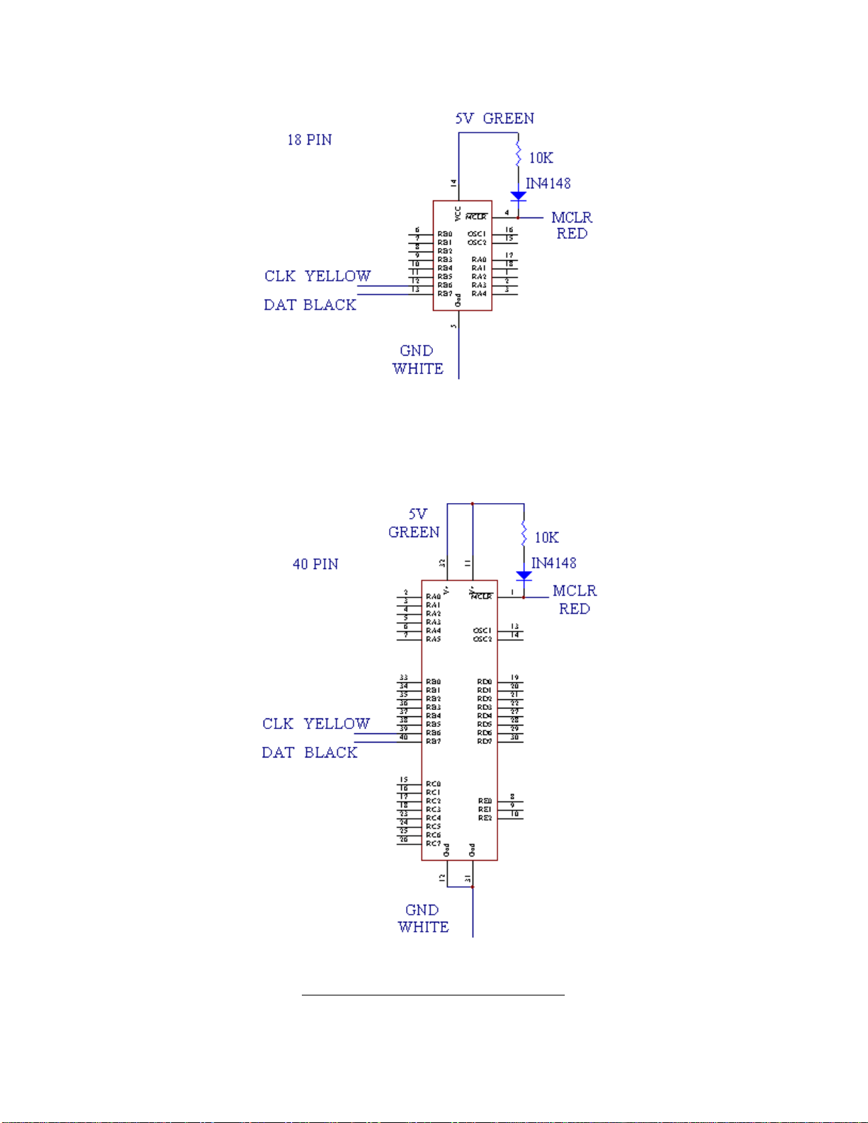
ICSP PROGRAMMING EXAMPLES

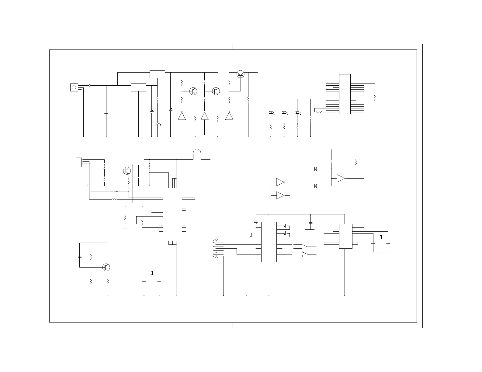
PARTS LIST
Used Part Type Designators Description
SEMICONDUCTORS
174LS06 U4 OC Hex Inverter
1ICL232 U3 RS232 transiever
1PIC16F628 U5 PIC Processor
1FT232BM U6 USB
1 78L08 U1 Regulator
1 7805 U2 Regulator
14MHz X1 Crystal
16MHz X2 Crystal
4BC558 TR1 TR2 TR3 TR5 PNP Transistor
1BC547 TR4 NPN Transistor
1IN4004 D2 Diode
2IN4148 D1 D3 Diode
1PWR L1 3mm LED
1VPP1 L4 3mm LED
1VPP2 L3 3mm LED
1VCCP L2 3mm LED
RESISTORS all 1/4W 5%
210R R20, R23
1 470R R25
51K R1, R4, R12, R13
11K5 R22
32K2 R5, R10, R15
13K3 R8
34K7 R11, R14 R16
810K R2, R3, R6, R7, R9 R21 R28, R29
122K R17
4100K R18, R19, R24, R26
1470K R27
CAPACITORS
4 22p C9, C10, C11, C12 Ceramic
110N C13 MKT
133N C15 MKT
4100N C7, C8, C14, C16 MKT
41uF C1 C3 C4 C5 Electrolytic 16V
110uF C2 Electrolytic 16V
147uF C6 Electrolytic 16V
MISCELLANEOUS
1BLANK PCB PCB1
1IC SOCKET 18 pin
1SERIAL CN1 Female RA DB9
1USB CN2 UT-5676
4FEET Rubber Feet
1JACK JK1 3 Pin Power Jack
1SWITCH SW1 DPDT
1HEATSINK
1SCREW & NUT
1 2 3 4 5 6
A
B
C
D
654321
D
C
B
A
C7
100N
X1
4MHz
C9
22p
C10
22p
Vcc
Vin
1
GND
2
Vout 3
U2
7805
Vin
1
GND
2
Vout 3
U1
78L08
Vcc
C2
10uF
1
2
3
4
5
6
7
8
9
10
11
12
13
14
15
16
17
18
19
20 21
22
23
24
25
26
27
28
29
30
31
32
33
34
35
36
37
38
39
40
SKT1
PROGRAMMER
C6
47uF
SVP1
SVP2
C8
100N
Gnd
Gnd
VON
R5
2K2
L2
VCCP
CS
L1
PWR
R8
3K3
R7
10K
PV
R3
10K
1
2
3
JK1
18VDC
L3
VPP2
L4
VPP1
R15
2K2 R10
2K2
SVP1
SVP2
VON
1
6
2
7
3
8
4
9
5
CN1
SERIAL
C3
1uF
C4
1uF
C1
1uF
C5
1uF
C1+ 1
C1- 3
C2+ 4
C2- 5
+10
2
-10
6
T1in 11
T2in 10
R1out 12
R2out 9
T1out
14
T2out
7
R1in
13
R2in
8
GND
15 VCC 16
U3
ICL232
Gnd
R14
4K7 R11
4K7
DATA
DATA
DATA
DATA
CLOCK
CLOCK
CLOCK
CLOCK
PV
CS
VPP1
VPP2
VPP2
Gnd
Gnd
Gnd
Gnd
Gnd
Gnd
Gnd
VccP
VccP
VccP
VccP
R1
1K
R12
1K R13
1K
TR3
BC558 TR1
BC558
R9
10K R2
10K
VPP1
VPP2
1 2
U4A
3 4
U4B
TR2
BC558
R6
10K
R4
1K
5 6
U4C
VON
SVP1
SVP2
Vcc VccP
Gnd
Gnd
VccP Gnd
Gnd
AVCC 30
VCC 3
VCC 13
VCC 26
USBDP
7
USBDM
8
3V3OUT
6
XTIN
27
XTOUT
28
RCCLK
31
RESET#
4
EECS
32
EESK
1
EEDATA
2
TEST
5
AGND
29
GND
9
GND
17
SLEEP# 10
RXLED# 11
TXLED# 12
PWRCTL 14
USBEN 15
TXDEN 16
RI# 18
DCD# 19
DSR# 20
DTR# 21
CTS# 22
RTS# 23
RXD 24
TXD 25
U6
FT232BM
1
2
3
4
CN2
USB
R20
10R
R23
10R
R25
470R
R22
1K5
R24
100K
R27
470K
R19
100K
R26
100K
TR5
BC558 X2
6MHz
C12
22p
C11
22p
C15
33N C14
100N
C16
100N
C13
10N
XA
XA
XB
XB
Vcc
URST
URST
UV
UV
Gnd
Gnd Gnd
TX
RX
UTX
URX
UTX
URX
RA0 17
RA1 18
RA2 1
RA3 2
RA4 3
RB0
6
RB1
7
RB2
8
RB3
9
RB4
10
RB5
11
RB6
12
RB7
13
MCLR 4
OSC1 16
OSC2 15
Gnd
5VCC 14
U5
16F628
RX
TX
CLOCK
DATA
9 8
U4D 11 10
U4E
13 12
U4F
D2
IN4004
TR4
BC547
R17
22K
R18
100K
UV
R28
10K MCLR
USBRST
74LS06
THIS LINK IS SOLDERED
IN POSITION AFTER THE
POWER CHECKS HAVE BEEN MADE
UV
1
2
LK1
USBPWR
R21
10K
Vcc
MCLR
USBRST
RS2RST
RS2RST S1
SERIAL USB
TXA
TXA
RXA
RXA
D3
1N4148
D1
1N4148
R16
4K7
Vcc
R29
10K
VccP
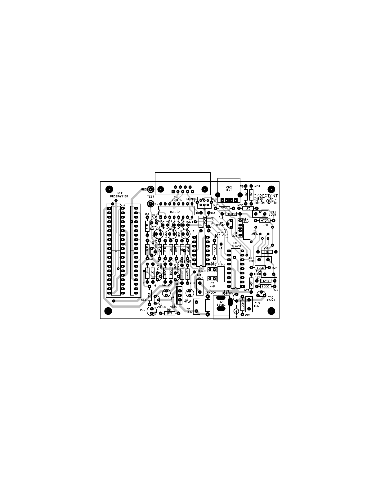


Table of contents
Other DIY Motherboard manuals


