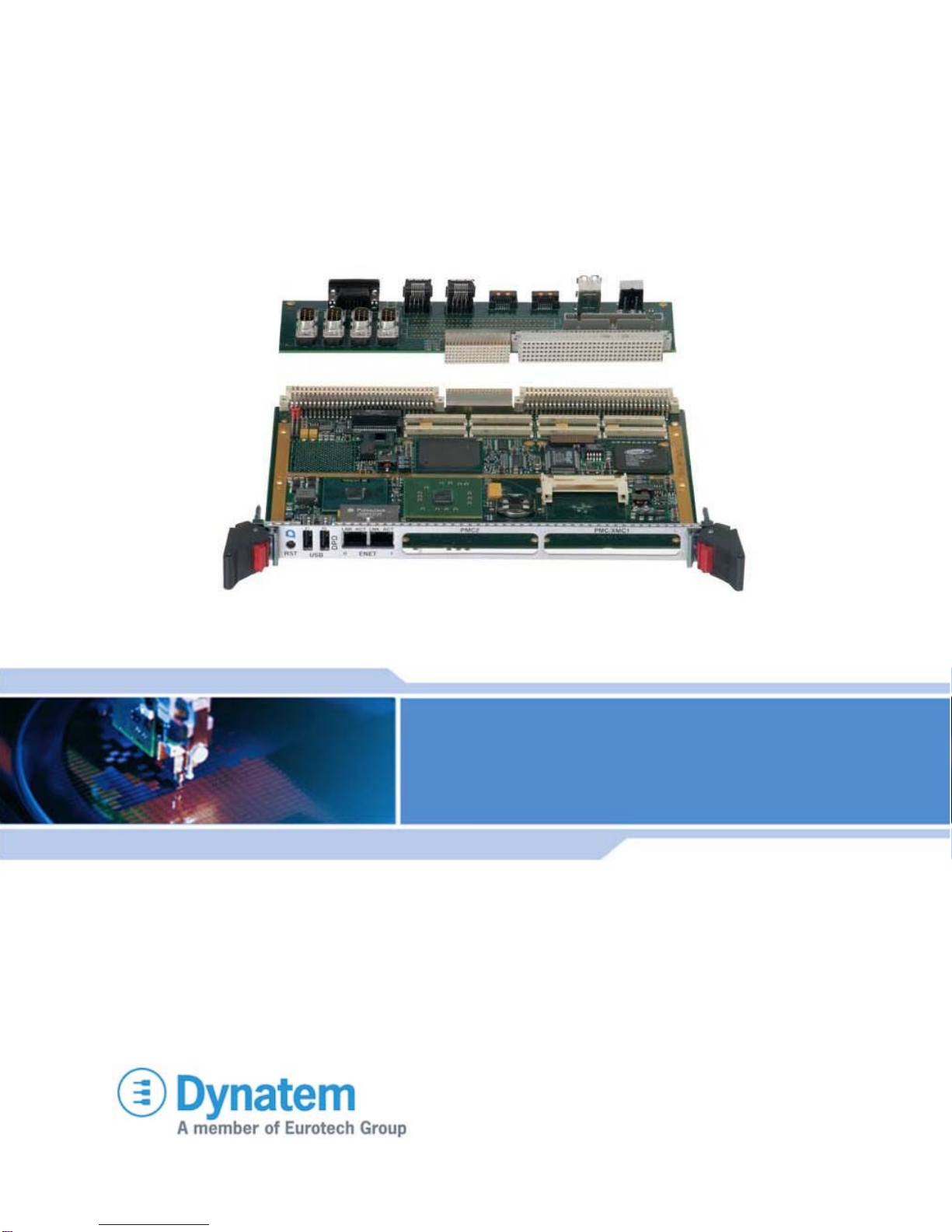
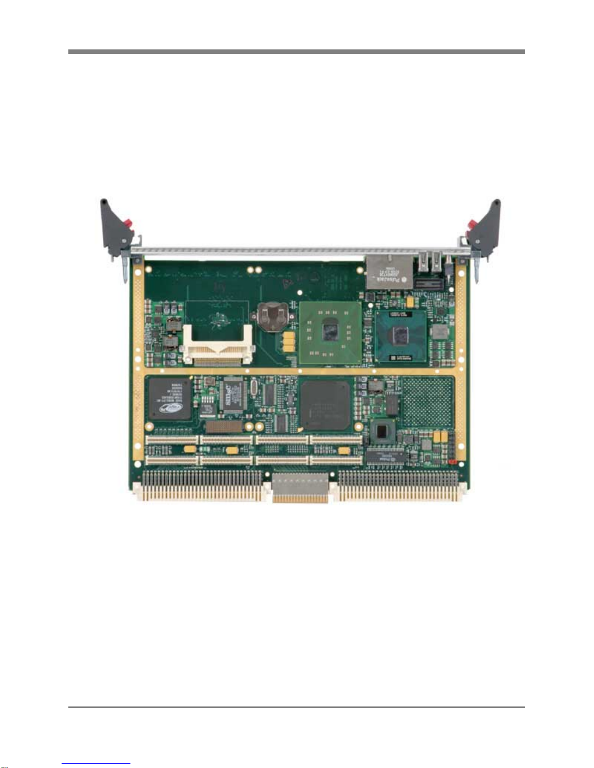
Chapter 3 – Hardware Description
6 CPU-71-10 (XPD/RPD/DPD) VMEbus Core 2 Duo Processor Board – User’s Manual
3.2 Processor
The XPD supports a Core Duo processor at 1.66 GHz. The Intel Core Duo processor with 2 MB of L2 cache is the
first dual core processor available for mobile and embedded applications. Features include:
667 MHz front side bus (limited by the E7520 FSB).
On-die 4 MB of L2 cache with Advanced Transfer Cache Architecture.
On-die, primary 32-KB instruction cache and 32-KB write-back data cache.
Second-generation Streaming SIMD Extensions 2 (SSE2) and streaming SIMD Extensions 3 (SSE3)
Supports Intel® Architecture and Dynamic Execution.
For further information on the Core2 Duo processor available from Intel Corporation, search at:
http://ark.intel.com/products/28026?wapkw=l7400
The Intel® Core™ Duo processor was designed to deliver high, dual processor high performance with low power
consumption. With its 65 nm processing technology and 2 MB of L2 advanced transfer cache, the Core Duo offers
more performance per Watt. The Thermal Design Power (TDP) is 15 W. Advanced power management included
Enhanced Intel SpeedStep Technology are supported. SpeedStep enables clock and core voltage throttling based on
temperature or processor loading.
The processor’s 667 MHz Front Side Bus utilizes a split-transaction, deferred reply protocol. The FSB uses a
Source-Synchronous Transfer (SST) of address and data to improve performance by transferring data four times per
bus clock. The address bus can deliver addresses twice per clock cycle. Together, the 4X data bus and 2X address
bus provide a data bus bandwidth of up to 5.33 GB/second.
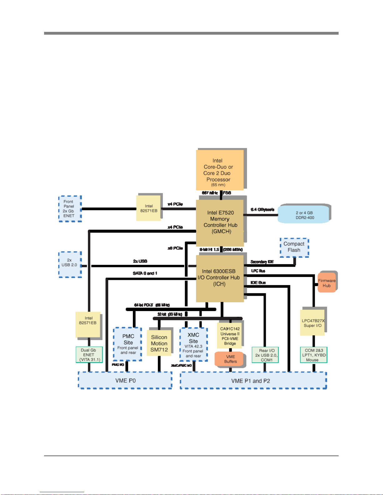
3.3 Chipset
The Intel® E7520 Memory Controller Hub (MCH) and Intel® 6300ESB I/O Controller Hub (ICH) chipset provide
memory control, mass storage and basic I/O, and standard PC system resources including the real time clock, NV-
RAM, timers, thermal management, and interrupt management. Also, the MCH provides 24 lanes of PCI Express
expansion (16 of which are implemented on the XPD) for high-speed expansion through the two dual 1000BaseTX
controller chips and the XMC site.. The ICH supports a 32 bit @ 33 MHz PCI bus, to support the Universe
VMEbus interface controller and the Silicon Motion SM712 graphics chip, and a 64 bit @ 66 MHz PCI-X bus for
user I/O expansion through the two PMC sites. The ICH also provides a Low Pin Count (LPC) interface for the
BIOS flash chip and for Super I/O and an SMBus interface for on-board resources like the DRAM circuit’s SPD
PROMs and the thermal monitors.
The MCH supports a base system bus frequency of 200 MHz. The address and request interface is double pumped
to 400 MHz while the 64-bit data interface (+ parity) is quad pumped to 800 MHz. This provides a matched system
bus address and data bandwidth of 6.4 GB/s. The E7520 (MCH) provides a 400 MHz interface to DDR2 RAM (72
bits wide with ECC). The XPD can be populated with one or two banks of DRAM for 2 GB or 4 GB of total
memory respectively. Each bank is serviced by a separate channel from the MCH that function in lock-step mode.
Memory controller features include:
Memory mirroring allows for two copies of all data in the memory subsystem (one on each channel) to be
maintained.
Hardware periodic memory scrubbing, including demand scrub support.