E-RM Neoverse N1 Product manual

Arm® Neoverse™ N1 System
Development Platform
Technical Reference Manual
Copyright © 2019, 2020 Arm Limited or its affiliates. All rights reserved.
101489_0000_02_en

Arm® Neoverse™ N1 System Development Platform
Technical Reference Manual
Copyright © 2019, 2020 Arm Limited or its affiliates. All rights reserved.
Release Information
Document History
Issue Date Confidentiality Change
0000-00 01 March 2019 Confidential Alpha1 release
0000-01 17 September 2019 Non-Confidential Alpha2 release.
0000-02 06 April 2020 Non-Confidential Beta release.
Non-Confidential Proprietary Notice
This document is protected by copyright and other related rights and the practice or implementation of the information contained in
this document may be protected by one or more patents or pending patent applications. No part of this document may be
reproduced in any form by any means without the express prior written permission of Arm. No license, express or implied, by
estoppel or otherwise to any intellectual property rights is granted by this document unless specifically stated.
Your access to the information in this document is conditional upon your acceptance that you will not use or permit others to use
the information for the purposes of determining whether implementations infringe any third party patents.
THIS DOCUMENT IS PROVIDED “AS IS”. ARM PROVIDES NO REPRESENTATIONS AND NO WARRANTIES,
EXPRESS, IMPLIED OR STATUTORY, INCLUDING, WITHOUT LIMITATION, THE IMPLIED WARRANTIES OF
MERCHANTABILITY, SATISFACTORY QUALITY, NON-INFRINGEMENT OR FITNESS FOR A PARTICULAR PURPOSE
WITH RESPECT TO THE DOCUMENT. For the avoidance of doubt, Arm makes no representation with respect to, and has
undertaken no analysis to identify or understand the scope and content of, third party patents, copyrights, trade secrets, or other
rights.
This document may include technical inaccuracies or typographical errors.
TO THE EXTENT NOT PROHIBITED BY LAW, IN NO EVENT WILL ARM BE LIABLE FOR ANY DAMAGES,
INCLUDING WITHOUT LIMITATION ANY DIRECT, INDIRECT, SPECIAL, INCIDENTAL, PUNITIVE, OR
CONSEQUENTIAL DAMAGES, HOWEVER CAUSED AND REGARDLESS OF THE THEORY OF LIABILITY, ARISING
OUT OF ANY USE OF THIS DOCUMENT, EVEN IF ARM HAS BEEN ADVISED OF THE POSSIBILITY OF SUCH
DAMAGES.
This document consists solely of commercial items. You shall be responsible for ensuring that any use, duplication or disclosure of
this document complies fully with any relevant export laws and regulations to assure that this document or any portion thereof is
not exported, directly or indirectly, in violation of such export laws. Use of the word “partner” in reference to Arm’s customers is
not intended to create or refer to any partnership relationship with any other company. Arm may make changes to this document at
any time and without notice.
If any of the provisions contained in these terms conflict with any of the provisions of any click through or signed written
agreement covering this document with Arm, then the click through or signed written agreement prevails over and supersedes the
conflicting provisions of these terms. This document may be translated into other languages for convenience, and you agree that if
there is any conflict between the English version of this document and any translation, the terms of the English version of the
Agreement shall prevail.
The Arm corporate logo and words marked with ® or ™ are registered trademarks or trademarks of Arm Limited (or its
subsidiaries) in the US and/or elsewhere. All rights reserved. Other brands and names mentioned in this document may be the
trademarks of their respective owners. Please follow Arm’s trademark usage guidelines at http://www.arm.com/company/policies/
trademarks.
Copyright © 2019, 2020 Arm Limited (or its affiliates). All rights reserved.
Arm Limited. Company 02557590 registered in England.
110 Fulbourn Road, Cambridge, England CB1 9NJ.
LES-PRE-20349
Arm® Neoverse™ N1 System Development Platform
101489_0000_02_en Copyright © 2019, 2020 Arm Limited or its affiliates. All rights
reserved.
2
Non-Confidential - Beta

Confidentiality Status
This document is Non-Confidential. The right to use, copy and disclose this document may be subject to license restrictions in
accordance with the terms of the agreement entered into by Arm and the party that Arm delivered this document to.
Unrestricted Access is an Arm internal classification.
Product Status
The information in this document is for a Beta product, that is a product under development.
Web Address
www.arm.com
Conformance Notices
This section contains conformance notices.
Federal Communications Commission Notice
This device is test equipment and consequently is exempt from part 15 of the FCC Rules under section 15.103 (c).
CE Conformity
The Waste Electrical and Electronic Equipment (WEEE) marking, that is, the crossed out wheelie-bin figure, indicates that this
product must not be disposed of with general waste within the European Union. To prevent possible harm to the environment from
uncontrolled waste disposal, the user is required to recycle the product responsibly to promote reuse of material resources. To
comply with EU law, you must dispose of the product in one of the following ways:
• Return it to the distributer where it was purchased. The distributer is required to arrange free collection when requested.
• Recycle it using local WEEE recycling facilities. These facilities are now very common and might provide free collection.
• If purchased directly from Arm, Arm provides free collection. Please e-mail [email protected] for instructions.
The CE Declaration of Conformity for this product is available on request.
The system should be powered down when not in use.
It is recommended that ESD precautions be taken when handling this product.
The product generates, uses, and can radiate radio frequency energy and may cause harmful interference to radio communications.
There is no guarantee that interference will not occur in a particular installation. If this equipment causes harmful interference to
radio or television reception, which can be determined by turning the equipment off or on, you are encouraged to try to correct the
interference by one or more of the following measures:
• Ensure attached cables do not lie across any sensitive equipment.
• Reorient the receiving antenna.
• Increase the distance between the equipment and the receiver.
• Connect the equipment into an outlet on a circuit different from that to which the receiver is connected.
• Consult the dealer or an experienced radio/TV technician for help.
Note
It is recommended that wherever possible shielded interface cables be used.
Arm® Neoverse™ N1 System Development Platform
101489_0000_02_en Copyright © 2019, 2020 Arm Limited or its affiliates. All rights
reserved.
3
Non-Confidential - Beta

Contents
Arm® Neoverse™ N1 System Development Platform
Technical Reference Manual
Preface
About this book ...................................................... ...................................................... 7
Feedback .................................................................................................................... 10
Chapter 1 Introduction
1.1 Precautions .............................................................................................................. 1-12
1.2 About the N1 SDP ................................................. ................................................. 1-13
1.3 The N1 SDP at a glance .......................................................................................... 1-14
1.4 Getting started .................................................... .................................................... 1-19
1.5 Accessing the ATX power cables ............................................................................ 1-20
Chapter 2 Hardware description
2.1 N1 SDP hardware .................................................................................................... 2-22
2.2 N1 SoC .................................................................................................................... 2-25
2.3 External power .................................................... .................................................... 2-27
2.4 Clocks ...................................................................................................................... 2-28
2.5 Resets .......................................................... .......................................................... 2-35
2.6 IOFPGA ......................................................... ......................................................... 2-37
2.7 HDLCD video ..................................................... ..................................................... 2-43
2.8 PCI Express and CCIX systems .............................................................................. 2-45
2.9 Chip to Chip communications .................................................................................. 2-48
2.10 UARTs .......................................................... .......................................................... 2-51
101489_0000_02_en Copyright © 2019, 2020 Arm Limited or its affiliates. All rights
reserved.
4
Non-Confidential - Beta

2.11 LEDs, switches, and buttons ......................................... ......................................... 2-55
2.12 Debug ...................................................................................................................... 2-59
Chapter 3 Configuration
3.1 Overview of the configuration process .................................. .................................. 3-61
3.2 Powerup and powerdown sequences ...................................................................... 3-62
3.3 Configuration files .................................................................................................... 3-64
3.4 Configuration switches .............................................. .............................................. 3-68
3.5 Use of reset push buttons ........................................................................................ 3-70
3.6 Command-line interface ............................................. ............................................. 3-71
Chapter 4 Programmers model
4.1 About this programmers model ....................................... ....................................... 4-75
4.2 N1 SDP memory maps ............................................................................................ 4-76
4.3 N1 SoC interrupt maps ............................................................................................ 4-95
4.4 System Security Control registers .................................... .................................... 4-105
4.5 Serial Configuration Control registers .................................................................... 4-119
4.6 APB system registers ............................................................................................ 4-197
4.7 APB energy meter registers .................................................................................. 4-206
4.8 UART memory addresses and control registers .................................................... 4-225
Appendix A Signal descriptions
A.1 UART headers .............................................. .............................................. Appx-A-229
A.2 UART DB9 connectors ................................................................................ Appx-A-231
A.3 N1-SoC JTAG connector ...................................... ...................................... Appx-A-232
A.4 Trace connector ............................................. ............................................. Appx-A-233
A.5 Front panel I/O header ........................................ ........................................ Appx-A-235
A.6 PCI Express and CCIX slots ........................................................................ Appx-A-236
A.7 C2C connector .............................................. .............................................. Appx-A-237
A.8 Power connectors ........................................................................................ Appx-A-238
Appendix B Revisions
B.1 Revisions .................................................. .................................................. Appx-B-240
101489_0000_02_en Copyright © 2019, 2020 Arm Limited or its affiliates. All rights
reserved.
5
Non-Confidential - Beta


About this book
This book describes the Arm® Neoverse™ N1 System Development Platform.
Intended audience
This book is written for experienced hardware and software developers. It enables demonstration of
coherent traffic between the N1 SoC and an accelerator daughterboard, and PCI Express Gen 4
development.
Using this book
This book is organized into the following chapters:
Chapter 1 Introduction
This chapter introduces the Arm Neoverse N1 System Development Platform (N1 SDP).
Chapter 2 Hardware description
This chapter describes the N1 SDP hardware.
Chapter 3 Configuration
This chapter describes the powerup and configuration process of the N1 SDP.
Chapter 4 Programmers model
This chapter describes the programmers model of the N1 SDP.
Appendix A Signal descriptions
This appendix describes the signals that are present at the N1 SDP ports.
Appendix B Revisions
This appendix describes the technical changes between released issues of this book.
Glossary
The Arm® Glossary is a list of terms used in Arm documentation, together with definitions for those
terms. The Arm Glossary does not contain terms that are industry standard unless the Arm meaning
differs from the generally accepted meaning.
See the Arm® Glossary for more information.
Typographic conventions
italic
Introduces special terminology, denotes cross-references, and citations.
bold
Highlights interface elements, such as menu names. Denotes signal names. Also used for terms
in descriptive lists, where appropriate.
monospace
Denotes text that you can enter at the keyboard, such as commands, file and program names,
and source code.
monospace
Denotes a permitted abbreviation for a command or option. You can enter the underlined text
instead of the full command or option name.
monospace italic
Denotes arguments to monospace text where the argument is to be replaced by a specific value.
monospace bold
Denotes language keywords when used outside example code.
Preface
About this book
101489_0000_02_en Copyright © 2019, 2020 Arm Limited or its affiliates. All rights
reserved.
7
Non-Confidential - Beta

<and>
Encloses replaceable terms for assembler syntax where they appear in code or code fragments.
For example:
MRC p15, 0, <Rd>, <CRn>, <CRm>, <Opcode_2>
SMALL CAPITALS
Used in body text for a few terms that have specific technical meanings, that are defined in the
Arm® Glossary. For example, IMPLEMENTATION DEFINED, IMPLEMENTATION SPECIFIC, UNKNOWN, and
UNPREDICTABLE.
Timing diagrams
The following figure explains the components used in timing diagrams. Variations, when they occur,
have clear labels. You must not assume any timing information that is not explicit in the diagrams.
Shaded bus and signal areas are undefined, so the bus or signal can assume any value within the shaded
area at that time. The actual level is unimportant and does not affect normal operation.
Clock
HIGH to LOW
Transient
HIGH/LOW to HIGH
Bus stable
Bus to high impedance
Bus change
High impedance to stable bus
Figure 1 Key to timing diagram conventions
Signals
The signal conventions are:
Signal level
The level of an asserted signal depends on whether the signal is active-HIGH or active-LOW.
Asserted means:
• HIGH for active-HIGH signals.
• LOW for active-LOW signals.
Lowercase n
At the start or end of a signal name, n denotes an active-LOW signal.
Additional reading
This book contains information that is specific to this product. See the following documents for other
relevant information.
Preface
About this book
101489_0000_02_en Copyright © 2019, 2020 Arm Limited or its affiliates. All rights
reserved.
8
Non-Confidential - Beta

Arm publications
•Arm® Neoverse™ N1 Core Technical Reference Manual (100616).
•Arm® CoreLink™ DMC
‑
620 Dynamic Memory Controller Technical Reference Manual
(100568).
•Arm® CoreLink™ MMU
‑
600 System Memory Management Unit Technical Reference Manual
(100310).
•Arm® CoreLink™ NIC
‑
400 Network Interconnect Technical Reference Manual (DDI 0475).
•Arm® CoreLink™ CMN
‑
600 Coherent Mesh Network Technical Reference Manual (100180).
•Arm® CoreLink™ TLX
‑
400 Network Interconnect Thin Links Supplement to Arm® CoreLink™
NIC
‑
400 Network Interconnect Technical Reference Manual (DSU 0028).
•Arm® CoreLink™ GIC
‑
600 Generic Interrupt Controller Technical Reference Manual
(100336).
•Arm® CoreLink™ GIC
‑
400 Generic Interrupt Controller Technical Reference Manual
(DDI 0471).
•Arm® Cortex®
‑
M7 Processor Technical Reference Manual (DDI 0489).
•Arm® PrimeCell UART(PL011) Technical Reference Manual (DDI 0183).
•Arm® PrimeCell General Purpose Input/Output (PL061) Technical Reference Manual
(DDI 0190).
•Arm® PrimeCell Real Time Clock (PL031) Technical Reference Manual (DDI 0224).
•Arm® Dual
‑
Timer (SP804) Technical Reference Manual (DDI 0271).
•Arm® Watchdog Module (SP805) Technical Reference Manual (DDI 0270).
•Arm® PrimeCell System Controller SP810 Technical Reference Manual (DDI 0254)
•Arm® CoreSight™ Components Technical Reference Manual (DDI 0314).
•Arm® DS
‑
5 Getting Started Guide (100950).
•Arm® DS
‑
5 Arm DSTREAM User Guide (100955).
•Arm® DS
‑
5 Debugger User Guide (100953).
The following book is only available to licensees or requires registration with Arm.
•Arm® DynamIQ™ Shared Unit Technical Reference Manual (100453).
Preface
About this book
101489_0000_02_en Copyright © 2019, 2020 Arm Limited or its affiliates. All rights
reserved.
9
Non-Confidential - Beta

Feedback
Feedback on this product
If you have any comments or suggestions about this product, contact your supplier and give:
• The product name.
• The product revision or version.
• An explanation with as much information as you can provide. Include symptoms and diagnostic
procedures if appropriate.
Feedback on content
If you have comments on content then send an e-mail to [email protected]. Give:
• The title Arm Neoverse N1 System Development Platform Technical Reference Manual.
• The number 101489_0000_02_en.
• If applicable, the page number(s) to which your comments refer.
• A concise explanation of your comments.
Arm also welcomes general suggestions for additions and improvements.
Note
Arm tests the PDF only in Adobe Acrobat and Acrobat Reader, and cannot guarantee the quality of the
represented document when used with any other PDF reader.
Preface
Feedback
101489_0000_02_en Copyright © 2019, 2020 Arm Limited or its affiliates. All rights
reserved.
10
Non-Confidential - Beta

Chapter 1
Introduction
This chapter introduces the Arm Neoverse N1 System Development Platform (N1 SDP).
It contains the following sections:
•1.1 Precautions on page 1-12.
•1.2 About the N1 SDP on page 1-13.
•1.3 The N1 SDP at a glance on page 1-14.
•1.4 Getting started on page 1-19.
•1.5 Accessing the ATX power cables on page 1-20.
101489_0000_02_en Copyright © 2019, 2020 Arm Limited or its affiliates. All rights
reserved.
1-11
Non-Confidential - Beta

1.1 Precautions
This section describes precautions that ensure safety and prevent damage to your N1 SDP.
This section contains the following subsections:
•1.1.1 Ensuring safety on page 1-12.
•1.1.2 Operating temperature on page 1-12.
•1.1.3 Preventing damage on page 1-12.
1.1.1 Ensuring safety
The N1 SDP is supplied in a mains-powered standard PC tower. A standard 5V ATX supply powers the
board.
Warning
• Do not use the N1 SDP near equipment that is sensitive to electromagnetic emissions, for example,
medical equipment.
• To reduce the risk of injury, ensure that the N1 SDP is powered down and that the fans have stopped
turning before opening the chassis.
1.1.2 Operating temperature
The N1 SDP has been tested in the temperature range 15°C‑30°C.
1.1.3 Preventing damage
The N1 SDP is intended for use within a laboratory or engineering development environment.
Caution
If you remove the N1 SDP from the PC tower, observe the following precautions:
• Never subject the board to high electrostatic potentials. Observe ElectroStatic Discharge (ESD)
precautions when handling any board.
• Always wear a grounding strap when handling the board.
• Only hold the board by the edges.
• Avoid touching the component pins or any other metallic element.
1 Introduction
1.1 Precautions
101489_0000_02_en Copyright © 2019, 2020 Arm Limited or its affiliates. All rights
reserved.
1-12
Non-Confidential - Beta

1.2 About the N1 SDP
The N1 SDP provides access to the Arm Neoverse N1 SoC.
N1 SoC and board
The N1 SDP enables software development for key enterprise technology and general Arm software
development.
The N1 SDP consists of the N1 board containing the N1 SoC. The N1 board is a micro-ATX form factor
board and is supplied in a standard PC tower unit. The N1 SoC contains two dual-core Arm Neoverse N1
processor clusters.
The system demonstrates Arm technology in the context of Cache-Coherent Interconnect for
Accelerators (CCIX) protocol by:
• Running coherent traffic between the N1 SoC and an accelerator card.
• Coherent communication between two N1 SoCs.
• Enabling development of CCIX-enabled FPGA accelerators.
1 Introduction
1.2 About the N1 SDP
101489_0000_02_en Copyright © 2019, 2020 Arm Limited or its affiliates. All rights
reserved.
1-13
Non-Confidential - Beta
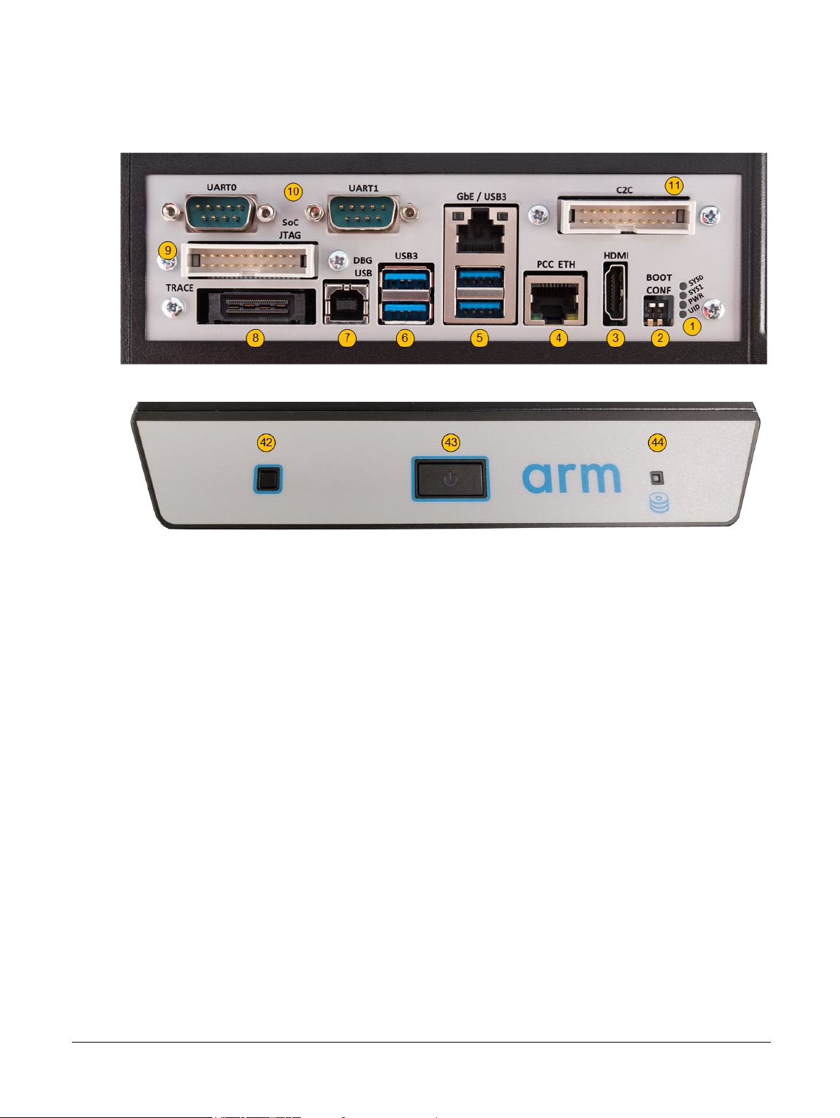
1.3 The N1 SDP at a glance
The following figures show the PC tower back panel and front panel, and the N1 board.
Figure 1-1 Back panel
Figure 1-2 Front panel reset buttons
1 Introduction
1.3 The N1 SDP at a glance
101489_0000_02_en Copyright © 2019, 2020 Arm Limited or its affiliates. All rights
reserved.
1-14
Non-Confidential - Beta

Figure 1-3 N1 board
The following table describes the components, connectors, and push buttons.
1 Introduction
1.3 The N1 SDP at a glance
101489_0000_02_en Copyright © 2019, 2020 Arm Limited or its affiliates. All rights
reserved.
1-15
Non-Confidential - Beta

Table 1-1 Key to figures
Component
number
Component name Access Comment
1 System LEDs Back panel. -
2 Configuration switches
3 HDMI port
4 PCC Ethernet port
5 GbE port. USB 3.0 ports.
6 USB 3.0 ports.
7 DBG USB port
8 N1 SoC trace port
9 N1 SoC JTAG port Ribbon cable to N1 SoC JTAG port, connector 17, on
board.
10 UART0 and UART1 DB9
male connectors
Arm supplies the N1 SDP with the following ribbon
cable connections:
• Header UART0 on board to DB9 connector UART0
on back panel.
• Header UART1 on board to DB9 connector UART1
on back panel.
The DB9 connectors are logically UARTs but the pins
follow the RS232 specification.
11 Chip-to-Chip (C2C)
Connector
Ribbon cable to Chip-to-Chip (C2C) connector, 19, on
board.
12 Slot 4: PCIe, CCIX, ×16
connector.
Board. Remove side
panel for access.
16 lanes used. Gen 4 link.
13 Slot 3: PCIe ×16 connector. 8 lanes used, 8 lanes unused. Gen 3 link.
14 Slot 2: PCIe ×16 connector. 16 lanes used. Gen 3 link.
15 Slot 1: PCIe ×4 connector. 1 lane used. 3 lanes unused. Gen 3 link.
16 ATX/EPS connector -
17 N1 SoC JTAG port Board. Ribbon cable to N1 SoC JTAG port, connector 9, on
back panel.
1 Introduction
1.3 The N1 SDP at a glance
101489_0000_02_en Copyright © 2019, 2020 Arm Limited or its affiliates. All rights
reserved.
1-16
Non-Confidential - Beta

Table 1-1 Key to figures (continued)
Component
number
Component name Access Comment
18 UART0, UART1, UART2,
and UART3 5×2 way
headers, no pin 10.
Board. Remove side
panel for access.
Arm supplies the N1 SDP with the following ribbon
cable connections:
• Header UART0 on board to DB9 connector UART0
on back panel.
• Header UART1 on board to DB9 connector UART1
on back panel.
Note
UART2 and UART3 headers are not connected to the
back panel.
The UART headers are logically UARTs but the header
pins follow the RS232 specification.
19 Chip-to-Chip (C2C)
Connector
Back panel Ribbon cable to Chip-to-Chip (C2C) connector, 11, on
back panel.
20 RDIMM1 memory Board. Remove side
panel for access.
-
21 RDIMM0 memory
22 ATX power connector and
power indicator LEDs
23 User switch SW8
24 User switch SW1
25 Reserved for use by Arm
26 IOFPGA microSD card
27 IOFPGA
28 User LED0
29 User LED7
30 Reserved for use by Arm
31 IOFPGA JTAG
32 Platform Controller Chip
(PCC)
33 7-segment display
34 Motherboard Configuration
Controller (MCC)
35 MCC configuration microSD
card
36 Front panel I/O connectors
37 PCIe SATA0
38 PCIe SATA1.
39 Reserved push button -
1 Introduction
1.3 The N1 SDP at a glance
101489_0000_02_en Copyright © 2019, 2020 Arm Limited or its affiliates. All rights
reserved.
1-17
Non-Confidential - Beta

Table 1-1 Key to figures (continued)
Component
number
Component name Access Comment
40 Hardware reset button,
PBRESET
Board. Remove side
panel for access.
The front panel I/O connector:
• Brings the PBON and PBRESET push button
functions to the front panel.
• Connects to the power LED.
41 On/Off/Soft reset push
button, PBON
42 Hardware reset button,
PBRESET
Front panel
43 On/Off/Soft reset push
button, PBON, and power
LED.
44 HDD activity LED. Combined signal from SATA0 and SATA1 from front
panel I/O connector on board.
1 Introduction
1.3 The N1 SDP at a glance
101489_0000_02_en Copyright © 2019, 2020 Arm Limited or its affiliates. All rights
reserved.
1-18
Non-Confidential - Beta

1.4 Getting started
The N1 SDP is controlled from a serial terminal that you connect to the DBG USB port. A set of files in
the non-volatile Motherboard Configuration Controller (MCC) configuration microSD card configures
the board. The configuration microSD card is accessible through the DBG USB port.
The board is factory-programmed with the MCC and Platform Controller Chip (PCC), System Control
Processor (SCP), Manageability Control Processor (MCP), and Application Processor (AP) firmware.
Powering up into the operating state
The minimum actions to boot the N1 SDP are as follows:
1. Connect a serial terminal to the DBG USB port on the back panel. The serial port settings must be:
• 115.2kBaud.
• 8N1.
• No hardware or software flow control.
By default, the four COM ports are connected to the following devices:
• COM<n> Motherboard Configuration Controller (MCC).
• COM<n+1> - Application Processor (AP).
• COM<n+2) - System Control Processor (SCP).
• COM<n+3) - Manageability Control Processor (MCP).
2. Turn the mains power switch on the PC tower ON. The MCC window command prompt is shown
and the system is now in the standby state. Ensure that both configuration switches on the back panel
are in the OFF (up) position. See 1.3 The N1 SDP at a glance on page 1-14 for the location of the
configuration switches.
3. To complete the powerup sequence from the standby state, briefly press the PBON button. The
system is now fully‑powered and in the operating state.
Editing configuration files
The configuration microSD card contains the system configuration files. To modify the system default
settings, edit or replace configuration files while the system is in standby state:
1. Ensure that the serial terminal is connected to the DBG USB port on the back panel.
2. Turn the power switch ON. The MCC window command prompt is shown and the system is now in
the standby state. Ensure that both configuration switches are in the OFF (up) position.
3. Issue the following command at the MCC command prompt on the serial terminal:
•Cmd> usb_on
The serial terminal now recognizes the configuration microSD card as a USB Mass Storage Device
(USBMSD).
4. Edit the existing configuration files, or Drag and Drop new files.
5. Perform a Hardware Reset by pressing the PBRESET button. The system is now in the standby state.
6. Briefly press the PBON button. The system is now fully powered and in the operating state.
Note
See 3.3 Configuration files on page 3-64 for information about the configuration files.
1 Introduction
1.4 Getting started
101489_0000_02_en Copyright © 2019, 2020 Arm Limited or its affiliates. All rights
reserved.
1-19
Non-Confidential - Beta

1.5 Accessing the ATX power cables
The N1 SDP PC tower provides SATA and other ATX power cables that you can use to connect to
external hard drives. The power cables are accessed by removing the metal side panel.
Warning
Before accessing the ATX power cables, ensure that the unit is disconnected from the mains power
supply.
Access the ATX power cables
To access the ATX power cables, you must gain access to the chassis:
1. Remove the large metal side panel:
• Undo the thumbscrews at the rear of the tower.
• Slide the side panel away from the tower.
2. The ATX power cables are now accessible, folded up inside the tower. Unfold the power cables to
connect them to external hard drives.
1 Introduction
1.5 Accessing the ATX power cables
101489_0000_02_en Copyright © 2019, 2020 Arm Limited or its affiliates. All rights
reserved.
1-20
Non-Confidential - Beta
Table of contents
Popular Computer Hardware manuals by other brands


ADLINK Technology
ADLINK Technology Q7-BT Technical reference

Hitachi
Hitachi F-ZTAT H8/3039 Series Hardware manual

Phanteks
Phanteks Glacier G1080 Ti Installation

JETWAY
JETWAY G03-BFDADN1QIG-F Quick installation manual

TBS technologies
TBS technologies TBS6301T user manual

Noctua
Noctua NF-A9 14 PWM Series user manual


