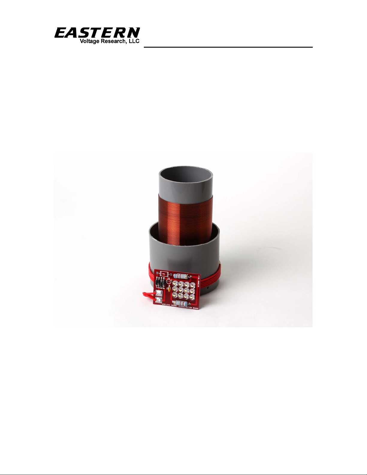
Wireless Energy Demonstration Kit
May 2012, Rev - − 7 − http://www.EasternVoltageResearch.com
Wireless Energy Demonstration Kit
electrical path through your heart providing you accidentally make contact
with live voltage.
Wear footwear with non-conductive (rubber) soles. Do NOT work on line
powered or high voltage equipment in barefeet.
Always wear eye protection. Power semiconductor devices, and capacitors do
have the potential to explode unexpectedly and project sharp fragments across
the room.
Always work in a clean, open area. Avoid working in cluttered spaces,
especially if there are grounded objects nearby that could complete a circuit
path in the event you make accidental contact with live voltage.
Avoid wearing any kind of jewelry or other articles that could accidentally
contact circuitry.
Never operate your PC boards on top of conductive tables, or other conductive
objects. PC boards should ALWAYS be supported by the provided stand-offs
or placed on top of a non-conductive tabletop or other material.
ALWAYS allow proper time for any large electrolytic or other high voltage
capacitors to discharge after removing power prior to working or touching any
circuit. ALWAYS use a multimeter to measure the voltage across large
capacitors after power is disconnect to ensure the voltage has properly bled
off.
Use an isolation transformer if there is any chance of contacting line powered
circuitry. A Variac is NOT an isolation transformer!
Finally, if your kit involves a Tesla Coil – NEVER touch or attempt to draw
an arc with an object from the output of a Tesla Coil. The output of a Tesla
Coil poses not only an electrical hazard, but also a burn hazard. The output
from even the smallest solid state Tesla Coil can cause serious burns. Always
operate the Tesla Coil at a safe distance.
SAFETY GUIDELINES - SEMICONDUCTOR POWER DEVICES
Always wear eye protection. Power semiconductor devices, and capacitors do
have the potential to explode unexpectedly and project sharp fragments across
the room.
Power semiconductors may be extremely hot. NEVER touch any
semiconductors during operation or after use. Always allow proper time for
components to cool down prior to handling them.