Echo Mountain Audio JBL 4425 User manual

JBL Model 4425
Charge-Coupled Crossover
User Manual
echomountainaudio.com
echo mountain audio
altadena, california

2
INTRODUCTION 2
THE CHARGE-COUPLED TOPOLOGY 3
WHAT YOU’LL NEED 3
OVERVIEW 4
PARTS INFORMATION 6
REMOVING CROSSOVER FROM SPEAKER 7
REMOVING FACTORY PCB FROM CROSSOVER UNIT 7
PCB ASSEMBLY 8
INSTALLATION OF PCBS INTO CROSSOVER ASSEMBLY 10
INSTALLATION OF COMPLETED CROSSOVER ASSEMBLIES 11
APPENDIX A: PARTS LIST 13
APPENDIX B: MEASURED FREQUENCY RESPONSE 14
Introduction
Thank you for your purchase of Echo Mountain Audio’s charge-coupled crossover boards for the
JBL Model 4425 Studio Monitor. The set of bare boards you have received are intended for DIY
build and “plug-and-play” integration into your existing 4425 monitor system.
The scope of this user manual is to, as succinctly as possible, guide the assembly of the PCBs
and integration into the existing crossover unit.
Any comments, questions, technical support requests, etc. are welcomed and encouraged, and

3
The Charge-Coupled Topology
The “charge-coupling” technique was first employed on JBL’s K2 S5500 loudspeaker system by
Chief Engineer Greg Timbers and was used subsequently on all high-end JBL Synthesis models,
including the top-of-the-line Everest DD66000. The technique involves replacing a given capacitor
in a crossover topology with two series capacitors of twice that value (this series combination is
equivalent to the original value), with a DC bias injected between the two capacitors through a
large value resistor. This DC-biased topology mitigates the effects of dielectric absorption and
the distortion associated with a change in the direction of current as the input signal transitions
from positive to negative (i.e., zero crossing). The theory of operation is explained in detail in the
following excerpts from the K2 S5500 product overview:
http://www.lansingheritage.org/images/jbl/specs/home-speakers/1993-k2-s5500/page10.jpg
http://www.lansingheritage.org/images/jbl/specs/home-speakers/1993-k2-s5500/page11.jpg
http://www.lansingheritage.org/images/jbl/specs/home-speakers/1993-k2-s5500/page12.jpg
What You’ll Need
To complete the project build, you’ll need the items listed below. Links for each item are
provided to the recommended items/brands we’ve used in our own builds, but feel free to use
what works best for you.
• (2) Echo Mountain Audio Model 4425 Crossover boards
• 4425 Charge-Coupled parts kit for Model 4425 from Solen (see Parts Information
section and Appendix A for more details)
• (2) 9V batteries
• (2) 9V battery holder clips
• (2) 9V battery connectors with flying leads
• Zip ties
• Soldering iron – The PACE ADS200 is excellent, made in the USA, and what we use
• Small, smooth-jaw (non-marring) pliers
• Wire cutters
• Wire strippers
• Eutectic (Sn63/Pb37) flux-core solder – not lead-free! We use Cardas solder.
• De-soldering pump
• Adhesive for staking large components (capacitors and inductors) to the PCB – we
highly recommend Eclectic Products E6000 Clear adhesive
• Heavy duty double-sided tape
4
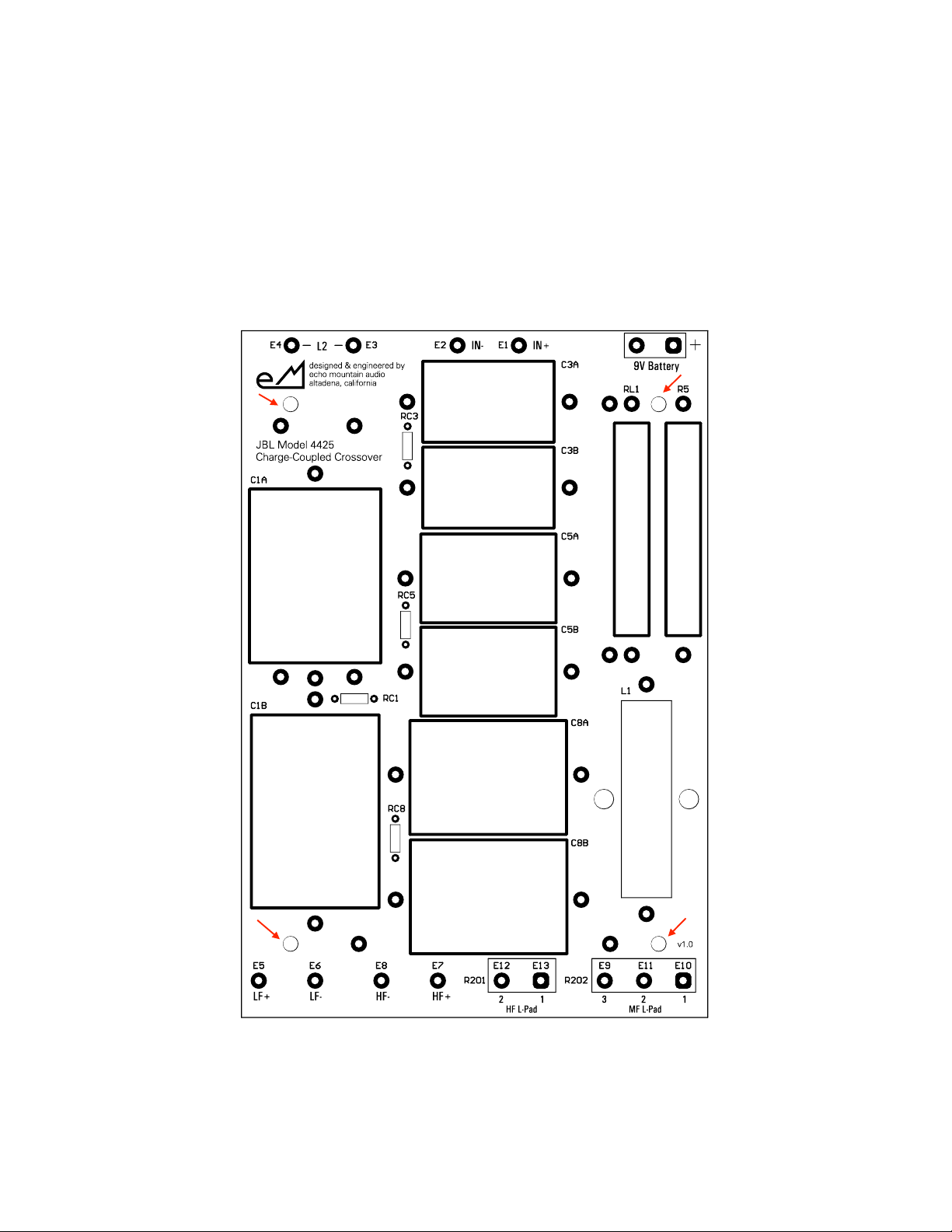
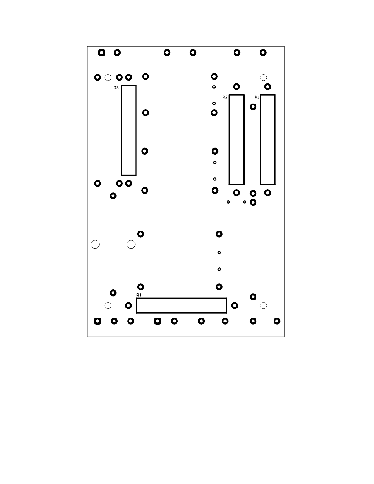
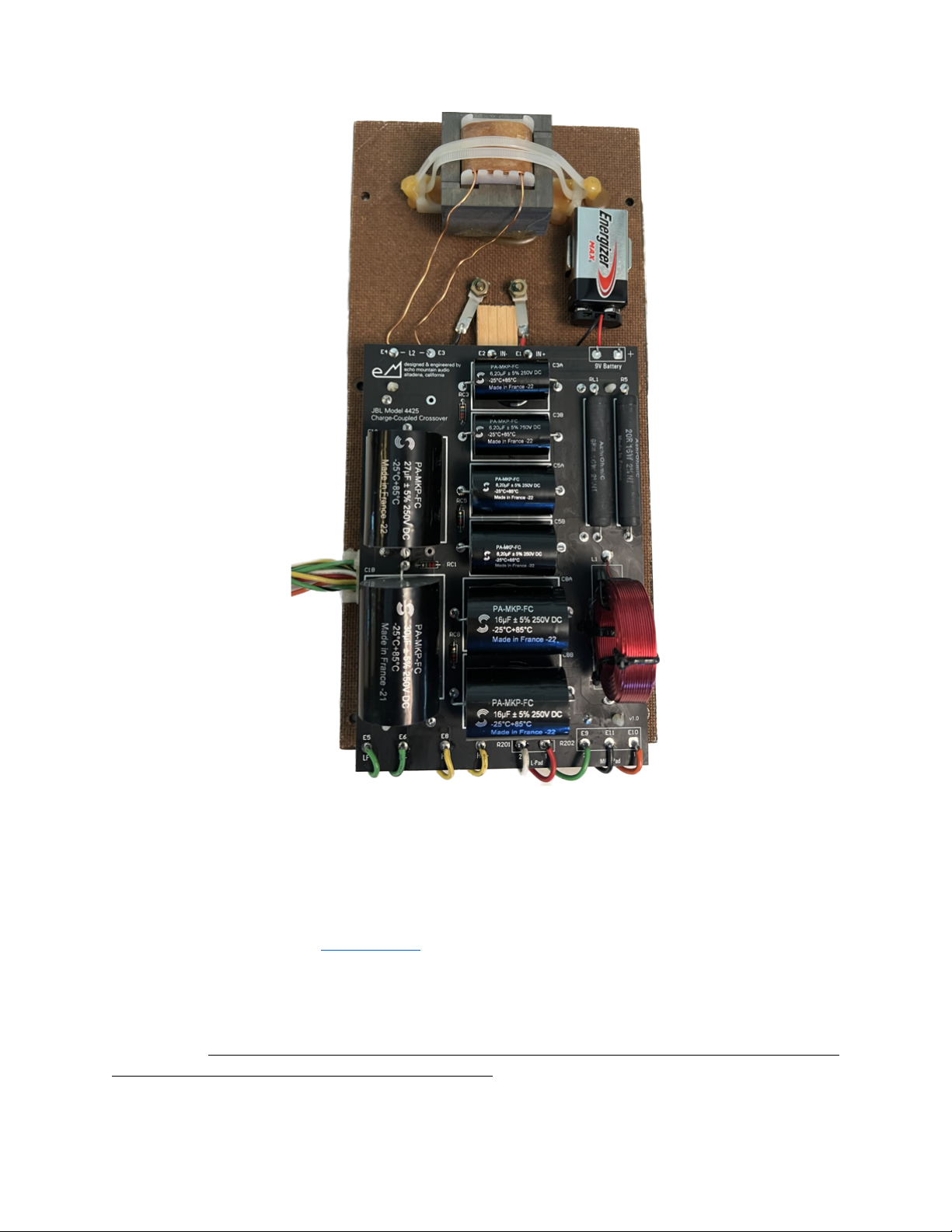
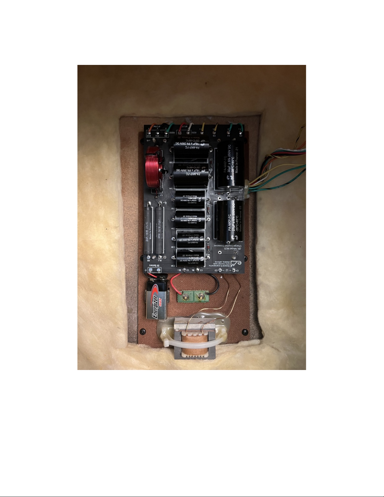
Overview
The JBL 4425 Charge-Coupled Crossover PCB is shown in Figure 1 (top side) and Figure 2
(bottom side). The board is designed to fit into the existing crossover housing, and the mounting
holes, denoted with red arrows in Figure 1, are sized to make use of the existing snap-lock PCB
clips. An example of a completed crossover, installed in the factory crossover housing, is shown
in Figure 3. Note that the default configuration uses the factory inductor for the woofer low-pass
filter. If you are building a custom crossover for the 4425, do not have access to a factory
crossover unit, and/or want to use a different inductor, please see the Parts Information section.
Figure 1: PCB top side view (mounting holes denoted with red arrows)
5
Figure 2: PCB bottom side view
6
Figure 3: Completed crossover unit with 9V battery installed
Parts Information
The footprints on the boards have been sized to accommodate the components in the official
parts kit from Solen in Canada. The contents of the parts kit are detailed in the Parts List in
Appendix A and on Solen’s product page.
Components of the same type and rating from other manufacturers may be substituted at the
user’s discretion, but it is the responsibility of the user to measure the board footprints and
ensure a proper fit, as well as ensuring that any user-substituted parts are properly rated for the
application. Echo Mountain Audio does not support or provide specific info on custom or user-
selected parts that are not on the official parts list.

7
Removing Crossover from Speaker
1. Lie the speaker on its back and remove the woofer by carefully loosening the screws
(don’t let the screwdriver slip and damage your cone or surround!) and lifting it gently out
of the cabinet.
2. Disconnect the two wires (green and green/black stripe) from the woofer and place the
woofer off to the side in a safe location.
3. You will now be able to see the stock crossover unit mounted to the rear wall of the
speaker. Now is a good time to take a picture of the stock units, wire orientation, etc., in
case you ever want to return the speaker to its stock configuration. Your new Echo
Mountain boards use the same pad numbering convention (E1, E2, E3, etc.) as the factory
boards for simplicity and ease of rework.
4. Unscrew the six Philips head screws that secure the mounting plate to the rear wall of
the speaker and set them aside in a safe place.
5. At this point, you’ll need to disconnect the wires going to the crossover unit in order to
be able to remove it from the cabinet. There are two options for this: de-soldering the
wires at the PCB (difficult because of the limited access through the woofer cutout), or
snipping the wires at the PCB (and then de-soldering the small bits of remaining wire once
the unit is removed). We strongly recommend the latter method, as it’s much easier, and
there is enough slack in the wires to allow for this. Snip the wires as close to the PCB as
possible (they should all be accessible from the top side of the board).
6. Once the wires are de-soldered or cut from the PCB, you will need to remove them from
the strain relief “clamp” that is adhered to the crossover mounting plate. This strain relief
apparatus doesn’t look the same on every model, but usually consists of adhesive, a zip
tie, or both. The adhesive is brittle enough due to years of age that it can be easily broken
and removed. Don’t worry about damaging the strain relief clamp, as you’ll be replacing
it later with an adhesive-backed zip tie mount and zip tie, but do take care not to damage
the wires.
7. At this point, the crossover assembly should be free of the speaker, and you should be
able to remove it through the woofer cutout.
8. Repeat steps 1-7 above for the other speaker.
Removing Factory PCB from Crossover Unit
1. Place the crossover unit on your workbench, and carefully release the PCB from the four
snap-lock plastic terminals by gently (gently!) pinching on the tabs with a pair of non-
marring pliers or your fingers. Do this to one corner at a time.
2. Once the PCB is free of the clips, locate the red and black wires connected between the
crossover binding posts and the PCB, and de-solder these wires from the PCB (leaving
them connected at the binding posts).
3. Locate the two wires coming from the inductor mounted on the crossover plate to the
PCB, and de-solder these wires from the PCB.
4. The factory PCB should now be free of the rest of the crossover assembly; set it aside.
5. Repeat steps 1 through 4 above for the other crossover unit.

8
PCB Assembly
For ease of assembly and to allow for unobstructed two-handed access to ensure that one makes
good solder joints, it is recommended to follow the steps in the order they are presented. Since
there are gluing and curing steps involved on the large components (capacitors and air core
inductor), we recommend doing each phase of the assembly in parallel on both boards before
moving on to the next phase, to minimize time spent waiting for the adhesive to cure. You’ll
notice that there is a mention of cleaning flux residue after each individual step – this is
intentional. As the board get populated with more components, it becomes more difficult to
clean off the flux residue in tight spaces, so do yourself a favor and clean it off after soldering
each component, before moving on to the next.
Note that because these PCBs contain plated through holes with annular rings on both sides of
the board, you are free to solder from either the top or bottom of the board. We recommend
soldering on the same side on which you are installing the component in question – it makes
things much easier.
It can also be helpful to install standoffs into the four mounting holes on the PCB to keep the
board stable while soldering. The standoffs can then be removed prior to installing the assembled
PCB back into the crossover unit.
Phase 1: Resistors
1. Insert and solder power resistors R1, R3, and R4 on the bottom side of the board. Note
that R2 will not be populated. Clean off any residual flux residue with a swab and
isopropyl alcohol.
2. Insert and solder the small 0.25W resistors RC1, RC3, RC5, RC8 on the top side of the
board. Clean off any residual flux residue with a swab and isopropyl alcohol.
3. Insert and solder power resistors RL1 and R5 on the top side of the board. Clean off any
residual flux residue with a swab and isopropyl alcohol.
Phase 2: Capacitors in the center of the board
In this phase, you will only install capacitors C3A, C3B, C5A, C5B, C8A, and C8B. These are the
six capacitors aligned vertically in the center of the board. Use the parts list in Appendix A to
locate the proper components for this section of the procedure.
1. Bend the leads of the capacitors using the plated through holes on the board as a sizing
guide and do a preliminary fit check of the capacitors in their footprints, adjusting your
lead bending as needed. Remove all the capacitors from the through holes once you’ve
done this.
2. Place a dab of adhesive in the center of the first PCB footprint (C3A). The general rule of
thumb is that less is more; you want enough adhesive to cover the entire surface area
where the capacitor touches the PCB, but be mindful that the adhesive will squeeze out
from under the component once you press it into place (we want this for mechanical
strength and vibration resistance), and you don’t want it getting all over the board or
squeezing into the adjacent footprints. See component C3A in the picture of the
completed assembly in Figure 3 for a reference of how much squeeze-out you’ll want.
3. After the adhesive has been applied, place capacitor C3A on the board with its leads
through the plated through holes and press down gently (don’t need much pressure) from

9
the top for a few seconds to allow the adhesive to spread underneath the part. The
component will have some play in the plated through holes, allowing it to rock and back
and forth slightly; adjust it so that it’s sitting upright and not tilted to one side.
4. Repeat steps 2 and 3 for the other five capacitor footprints (C3B, C5A, C5B, C8A, C8B).
Note that you’ll need a little more adhesive as the components get larger.
5. Now that all six of these capacitors are placed on the board, take a break and let the
adhesive cure for a while before proceeding to solder them all in. If you are using the
E6000 adhesive we recommended earlier in this manual, the advertised cure time is 24
hours for a full cure, but depending on the temperature in your work area, one hour or
slightly more should allow for a sufficiently stable bond to start soldering.
6. Solder the leads for the six capacitors you’ve installed so far and clean off all the flux
residue when you are done.
Phase 3: Capacitors C1A and C1B
1. Locate the 27µF and 30µF capacitors for positions C1A and C1B.
2. Follow the same procedure from steps 1 through 3 in Phase 2 to install these capacitors.
Phase 4: Inductor L1
1. Locate the 1.0mH air core inductor for position L1.
2. Start by doing a fit check -arrange the leads to fit through the plated through holes, while
positioning the inductor so that it sits flat on the board (see Figure 3 for reference). The
leads will be much longer than required for the given footprint, so trim off the excess
length, leaving enough to pass through the board and allow for a solder fillet on both
sides.
3. Now that you’ve trimmed off the excess leads to the desired length, you’ll need to
remove the enamel coating at the ends of the wire and tin the wire, so that it will solder
properly to the pads. This YouTube video provides a great tutorial on how to do this.
4. With the inductor removed from the board, thread a zip tie through the two holes on the
inductor footprint such that the zip tie is looped through the bottom of the board, and both
ends of the zip tie are pointing upwards. Leave the zip tie open for now.
5. As you did with the capacitors previously, place a dab of adhesive on the inductor
footprint, big enough that it will cover the mounting surface of the inductor with the
squeeze out, but not big enough that it will make a mess.
6. Place the inductor onto the footprint, with the leads inserted into the plated through holes,
and press down gently in the center to seat it in the adhesive. Carefully fasten the zip tie
so that it will clamp around the lower portion of the coil that is resting flush against the
board, tighten the zip tie, and snip off the excess. Allow the adhesive to cure for about
an hour before proceeding to the next step.
7. Solder the two inductor leads to the PCB.
At this point, you should now have two fully assembled boards with all capacitors and inductors
soldered and adhered to the board. Walk away, take a well-earned break, have an adult beverage,
etc., and allow all of the adhesive to cure for the full recommended cure time overnight before
proceeding to install the boards into the crossover assemblies.

10
Installation of PCBs Into Crossover Assembly
After allowing the boards to cure overnight, you’re now ready to install the new PCBs into the
factory crossover assembly.
1. Align the PCB mounting holes with the four snap-lock board mounts on the crossover
board, and gently snap each corner into place, one at a time. The board orientation should
match that shown in Figure 3.
2. Insert the stripped ends of the black and red wires from the binding posts into the plated
through holes E1 (IN+, red wire) and E2 (IN-, black wire). Solder both wires to the PCB.
3. Insert the tinned ends of the two wires from the inductor mounted on the crossover
assembly to pads E3 and E4 (also denoted by “L2” on the PCB silkscreen). Solder both
wires to the PCB.
4. Obtain one of the 9V battery connectors with flying leads. Cut the leads down to about
1-1.5 inches in length, strip the ends, and insert the red wire into the PCB pad marked 9V
battery “+” (upper right corner of the PCB). Insert the black wire into the PCB pad to the
left of that. Solder both wires to the PCB.
5. Obtain one of the 9V battery clips and the double-sided tape and cut a piece of tape to fit
to the bottom surface of the mounting clip. Affix one side of the tape to the bottom of
the clip and press down to adhere.
6. Place a 9V battery in the clip, center it, and then remove the protective layer on the
exposed side of double-sided tape. Place the battery and clip down on the right side of
the crossover assembly mounting plate, choosing the location such that there is enough
room to remove/install the battery, and enough room to attach the battery connector and
wires. Use Figure 3 as a guide on placement. Remove the battery from the clip while
holding the clip down to the surface (you don’t want to lift the tape up inadvertently).
Press down firmly on the bottom of the clip to increase the adhesion of the tape. If the
tape accidentally lifts from the crossover, start over with a fresh piece of tape, as it will
take small debris from the fiberboard with it, and won’t adhere as well on the next
attempt. This may sound complicated from the detailed description, but it’s quite simple.
Note that the battery can slide back and forth in the clip, so the exact placement of the
clip is not critical.
7. If remnants of the old strain relief clamp (refer to Step 6 of the “Removing Crossover
from Speaker” section) are still in place, remove them carefully with a putty knife or other
tool (the old, brittle adhesive should chip away easily). If this is proving difficult, leave it
there and move to the next step.
8. In the location of the old strain relief clamp (or adjacent to it, if you couldn’t get it fully
removed), place an adhesive-backed zip tie mount and press down to adhere.
9. Repeat steps 1 through 8 for the other PCB and crossover assembly.
11
Installation of Completed Crossover Assemblies
1. Inside the speaker cabinet, strip the ends of the L-pad and driver wires that were
previously snipped away from the factory PCB, twist the strands together, and tin the
ends of the wires with solder.
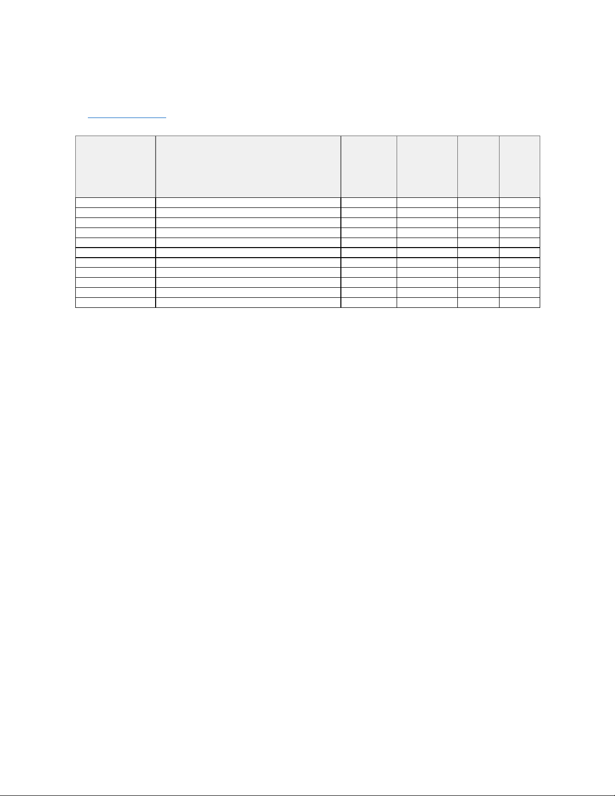
2. Solder the wires inside the cabinet to their proper PCB pads according to the table below.
The wire color codes shown in the table are consistent both with the 4425 speakers
we’ve tested and the original 4425 technical manual from JBL. Route the wires along the
bottom side of the board, bring them up and around the bottom edge of the PCB, and
Insert the wires into the PCB pads from the top side of the board – this will offer strain
relief of these connections (again, use Figure 3 as an example of how it should look).
Double check the wiring against the table below, and then solder the wires to the PCB.
3. Thread a zip tie through the zip tie mount you adhered to the assembly in the previous
section, so that it’s facing up. Bundle the wires from the bottom side of the PCB together
and use the zip tie to secure the bundle. Before tightening it fully, make sure there is no
excessive strain on the connections to the PCB, nor excess slack in the wire routing
underneath the PCB. You can push/pull the wires through your semi-tightened zip tie
loop until you have everything dressed properly, and then tighten it fully and snip off the
excess length.
4. Align the assembly mounting holes with their mounting points on the back wall of the
speaker and use the six original Philips head screws to securely mount the assembly to
the cabinet. An example of a finished, mounted assembly is shown in Figure 4.
5. Connect the green wire from the crossover to the red (+) terminal on the woofer and
connect the green/black striped wire to the black (-) terminal on the woofer.
6. Lower the woofer in to the cabinet, align the holes on the woofer with the holes on the
baffle, and use the original mounting screws to secure it.
7. Repeat steps 1 through 6 for the other crossover assembly and speaker cabinet.
8. You’re all done! Fire up some tunes and enjoy the upgraded sonic experience!
PCB Pad
Designator
Connection
E1 Red wire to speaker input +
E2 Black wire to speaker input -
E3 Enameled wire from stock inductor
E4 Enameled wire from stock inductor
E5 Green wire to LF driver red terminal
E6 Green/black wire to LF driver black terminal
E7 Yellow wire to HF driver red terminal
E8 Yellow/black wire to HF driver black terminal
E9 Green wire to L-Pad R202 pin 3
E10 Orange wire to L-Pad R202 pin 1
E11 Black wire to L-Pad R202 pin 2
E12 White wire to L-Pad R201 pin 2
E13 Red wire to L-Pad R201 pin 1
12
Figure 4: Completed crossover installed in speaker cabinet, as viewed through woofer cutout (top of image points
towards top of speaker)
13
Appendix A: Parts List
The table below shows the parts list included in the official parts kit from Solen (sold separately
on Solen’s website).
Designator Description Manufacturer
Manufacturer
Part No.
Quantity
per board
Total
Quantity
per
project
C1A Capacitor, 27 uF, PA Series, 250V Solen PA2700 1 2
C1B Capacitor, 30 uF, PA Series, 250V Solen PA3000 1 2
C3A, C3B Capacitor, 6.2 uF, PA Series, 250V Solen PA620 2 4
C5A, C5B Capacitor, 8.2 uF, PA Series, 250V Solen PA820 2 4
C8A, C8B Capacitor, 16 uF, PA Series, 250V Solen PA1600 2 4
L1 Inductor, 1.0 mH, Air Core Solen S201.0 1 2
R1 Resistor, 51 ohm, 16W, Non-inductive wirewound AchrOhmiC AOC1600G51R 1 2
R3 Resistor, 3.9 ohm, 16W, Non-inductive wirewound AchrOhmiC AOC1600G3R9 1 2
R4, R5 Resistor, 20 ohm, 16W, Non-inductive wirewound AchrOhmiC AOC1600G20R 2 4
RC1, RC3, RC5, RC8 Resistor, 2.2 Mohm, 0.25W, Carbon film Solen RCC025225J 4 8
RL1 Resistor, 6.8 ohm, 16W, Non-inductive wirewound AchrOhmic AOC1600G6R8 1 2
14
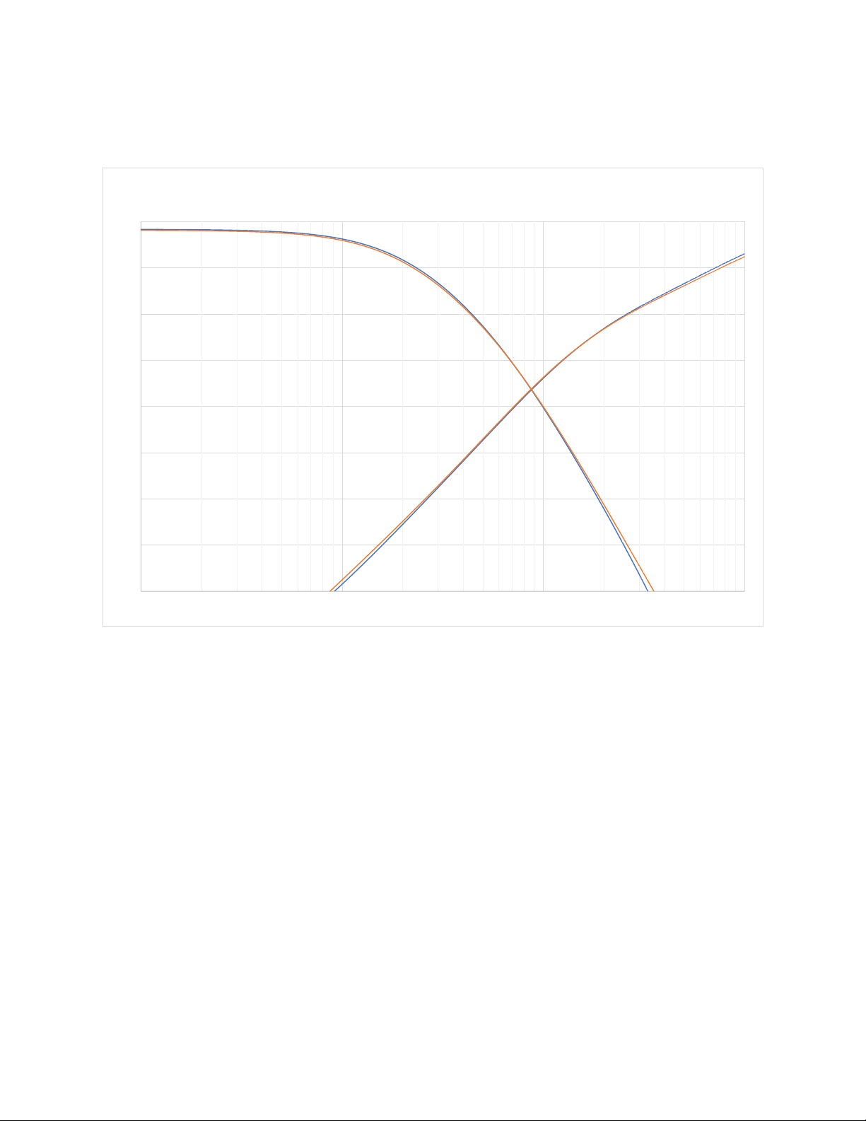
Appendix B: Measured Frequency Response
Measured response for the 4425 factory crossover (orange curves) and the Echo Mountain
Charge-Coupled Crossover (blue curves) was obtained using 8 ohm dummy loads with an RME
ADI-2 Pro FS R BE audio interface and REW software.
-40
-35
-30
-25
-20
-15
-10
-5
0
20 200 2000 20000
Magnitude (dB)
Frequency (Hz)
Model 4425 Crossover
Stock (Orange) vs. Echo Mountain Charge-Coupled Equivalent (Blue)
Both L-Pads at Max
Table of contents


