ELECTOR MCCAB User manual

1
Operating Instructions
Elektor Arduino®NANO
Training Board MCCAB
Rev. 3.3
Elektor

2
Dear customer,
The MCCAB Training Board is manufactured in accordance with the applicable European direc-
tives and therefore bears the CE mark.
Its intended use is described in these operating instructions. If you modify the MCCAB Training
Board or do not use it in accordance with its intended purpose, you alone are responsible for
compliance with the applicable rules.
Therefore, only use the MCCAB Training Board and all components on it as described in these
operating instructions. You may only pass on the MCCAB Training Board together with this
operating manual.
All information in this manual refers to the MCCAB Training Board with the edition level
Rev. 3.3. The edition level of the Training Board is printed on its bottom side (see Figure 13
on page 20).
The current version of this manual can be downloaded from the website
www.elektor.com/20440 for download.
ARDUINO®and other Arduino brand names and logos are registered trademarks of
Arduino SA.
Table of Contents
1Recycling.............................................................................................................3
2Safety instructions................................................................................................3
2.1 Power supply..................................................................................................3
2.2 Handling and environmental conditions..............................................................4
2.3 Repair and maintenance ..................................................................................4
3Intended use........................................................................................................5
4The MCCAB Training Board and its components........................................................6
4.1 The Arduino®NANO microcontroller module .......................................................8
4.2 The power supply of the MCCAB Training Board ................................................11
4.3 The USB connection between the MCCAB Training Board and the PC ...................13
4.4 The eleven LEDs D2 ... D12 for status indication of the microcontroller’s GPIOs ....13
4.5 The potentiometers P1 and P2........................................................................14
4.6 The switches S1 ... S6 and the buttons K1 ... K6...............................................15
4.7 The piezo buzzer Buzzer1...............................................................................16
4.8 The 3
×
3 LED matrix.....................................................................................17
4.9 The LC-Display (LCD) ....................................................................................19
4.10 The driver outputs SV1 and SV7 for higher output currents and voltages .............20
4.11 The SV2 socket connector for linking external modules......................................21
4.12 The pin headers for the connection of SPI modules............................................22
4.12.1 The interface SV11 for SPI modules with +3.3 V operating voltage...............23
4.12.2 The interface SV12 for SPI modules with +5 V operating voltage..................23
4.12.3 Simultaneous connection of SPI modules to SV11 and SV12 ........................24
4.13 The pin headers SV8, SV9 and SV10 for the TWI (=I2C) interface .......................25
5Hints for the use of the ATmega328P’s analog/digital converter................................26
6The Library "MCCAB_Lib" for the MCCAB Training Board ..........................................27
7Further Literature on the Use of the MCCAB Training Board......................................27

3
1Recycling
Used electrical and electronic equipment must be recycled as electronic waste and
must not be disposed of in household waste.
The MCCAB Training Board contains valuable raw materials that can be recycled.
Therefore, dispose of the device at the appropriate collection depot. (EU Directive
2012/19 / EU). Your municipal administration will tell you where to find the nearest
free collection point.
2Safety instructions
These operating instructions for the MCCAB Training Board contain important information on
commissioning and operation!
Therefore, read the entire operating manual carefully before using the training board
for the first time in order to avoid injury to life and limb due to electric shock, fire or
operating errors as well as damage to the Training Board.
Make this manual available to all other users of the training board.
The product has been designed in accordance with the IEC 61010-031 standard and has been
tested and left the factory in a safe condition. The user must observe the regulations applicable
to the handling of electrical equipment, as well as all generally accepted safety practices and
procedures. In particular, the VDE regulations VDE 0100 (planning, installation and testing of
low-voltage electrical systems), VDE 0700 (safety of electrical equipment for domestic use)
and VDE 0868 (equipment for audio/video, information and communication technology) should
be mentioned here.
In commercial facilities, the accident prevention regulations of commercial employers' liability
insurance associations also apply.
Safety symbols used
Electrical Hazard Warning
This sign indicates conditions or practices that could result in death or personal injury.
General Warning Sign
This sign indicates conditions or practices that may result in damage to the product
itself or to connected equipment.
2.1 Power supply
Caution:
Under no circumstances may negative voltages or voltages greater than +5 V be
connected to the MCCAB Training Board. The only exceptions are the inputs VX1
and VX2, here the input voltages may be in the range of
+8 V to +12 V (see section
4.2).
Never connect any other electrical potential to the ground line (GND, 0 V).
4
Never interchange the connections for ground (GND, 0 V) and +5 V, as this
would result in permanent damage to the MCCAB Training Board!
In particular, never conne
ct ~230 V or ~115 V mains voltage to the MCCAB
Training Board!
There is a danger to life !!!
2.2 Handling and environmental conditions
To avoid death or injury and to protect the device from damage, the following rules
must be strictly
observed:
Never operate the MCCAB Training Board in rooms with explosive vapors or gases.
If young people or persons who are not familiar with the handling of electronic
circuits work with the MCCAB Training Board, e.g., in the context of training, ap-
propr
iately trained personnel in a responsible position must supervise these activi-
ties.
The use by children under 14 years of age is not intended and must be avoided.
If the MCCAB Training Board shows signs of damage (e.g., due to mechanical or
electrical stress), it must not be used for safety reasons.
The MCCAB Training Board may only be used in a clean and dry environment at
temperatures up to +40 °C.
2.3 Repair and maintenance
To avoid damage to property or personal injury, any repairs that may become nec-
essary may only be carried out by appropriately trained specialist personnel and
using original spare parts.
The MCCAB Training Board does not contain any user-serviceable parts.
5
3Intended use
The MCCAB Training Board has been developed for simple and fast teaching of knowledge
about programming and the use of a microcontroller system.
The product is designed exclusively for training and practice purposes. Any other use, e.g., in
industrial production facilities, is not permissible.
Caution:
The
MCCAB Training Board is only intended for use with an Arduino® NANO micro-
controller syste
m (see Figure 2
) or a microcontroller module that is 100% compatible
with it. This module must be operated with an operating voltage of Vcc = +5V. Oth-
erwise, there is a risk of irreversible damage or destruction of the microcontroller
module, the training board and the devices connected to the training board.
Caution:
Voltages in the range
of
+8 V to +12 V may be connected to the inputs VX1 and VX2
of the training board (see section
4.2 of this manual).
The voltages at all other
inputs of the
training board must be in the range 0 V to +5 V.
Caution:
These operating instructions describe how to correctly connect and operate the
MCCAB Training Board with the user's PC and any external modules. Please note that
we have no influence on operating
and/or connection errors caused by the user.
The user alone is responsible for the correct connection of the training board to the
user's PC and any external modules, as well as for its programming and proper op-
eration!
For all damages resulting from wrong connection, wrong control, wrong programming
and / or wrong operation the user is solely responsible! Liability claims against us are
understandably excluded in these cases.
Any use other than that specified is not permitted! The MCCAB Training Board must not be
modified or converted, as this could damage it or endanger the user (short circuit, risk of
overheating and fire, risk of electric shock). If personal injury or damage to property occurs
as a result of improper use of the training board, this is the sole responsibility of the operator
and not of the manufacturer.

6
4The MCCAB Training Board and its components
Figure 1 shows the MCCAB Training Board with its control elements. The training board is
simply placed on an electrically non-conductive work surface and connected to the user's
PC via a mini-USB cable (see section 4.3).
Especially in combination with the "Microcontrollers Hands-On Course for Arduino Starters"
(ISBN 978-3-89576-545-2), published by Elektor, the MCCAB Training Board is perfectly
suited for easy and fast learning of programming and usage of a microcontroller system.
The user creates his exercise programs for the MCCAB Training Board on his PC in the Arduino
IDE, a development environment with an integrated C/C++ compiler, which he can download
free of charge from the website
https://www.arduino.cc/en/main/software
After its successful compilation, the exercise program is loaded from the Arduino IDE into the
microcontroller on the MCCAB Training Board via a mini USB cable and started directly.
Already "on board" on the MCCAB Training Board is an extensive hardware periphery (buttons,
switches, potentiometers, buzzers, indicators, display, serial interfaces, transistor switches),
which provides the necessary control elements for a variety of exercises. Furthermore, exter-
nal circuit boards and modules for additional exercise units can be connected to the training
board via the socket connector SV2 (arrow (26) in Figure 1).
To control external sensors, modules and devices that can be docked to the training board via
the various connector strips, a comprehensive collection of libraries is available in the "Arduino
world". These libraries can usually be downloaded free of charge from the Internet and inte-
grated into the user's training program.
The MCCAB Training Board works with an operating voltage of Vcc = +5 V. The training board
is usually supplied with power via the USB interface of the connected PC, which is also required
for creating the exercise programs. Alternatively, power can be supplied by an external power
supply unit (see section 4.2 and section 4.3).
The following Figure 1 shows the view of the training board. All hardware components on the
board are described in detail below.

7
Figure 1: The MCCAB Training Board, Rev. 3.3
The operating and display elements on the MCCAB Training Board:
(1) 11 ×LED (status indication for the in-
puts/outputs D2 ... D12)
(2) Header JP6 for connecting the LEDs
LD10 ... LD20 with the GPIOs
D2 ... D12 assigned to them
(3) Terminal block SV5 (distributor) for
the inputs/outputs of the microcon-
troller
(4) RESET button
(5) Microcontroller module Arduino®
NANO (or compatible) with mini USB -
socket
(6) LED "L", connected to GPIO D13
(7) Connector SV6 (distributor) for the
microcontroller inputs/outputs
(8) Potentiometer P1
(9) Pin header JP3 for selecting the oper-
ating voltage of potentiometers P1
and P2
(10) Potentiometer P2
(11) Pin header JP4 for selecting the sig-
nal at pin X of connector strip SV12
(12) Connector strip SV12: SPI-Interface
5 V (the signal at pin X is selected
via JP4)
(13) Connector strip SV11:
SPI interface 3.3 V
(14) Terminal block SV10:
I2C interface 5 V
(15) Terminal block SV8:
I2C interface 3.3 V
(16) Terminal block SV9:
I2C interface 3.3 V
(17) Terminal block SV7: Switching out-
put for external devices
(18) LC display with 2 x 16 characters
(19) 6 ×pushbutton switches K1 ... K6

8
(20) 6 ×slide switches S1 ... S6
(21) Pin header JP2 for connecting the
switches to the inputs of the micro-
controller.
(22) Terminal block SV4: distributor for
the operating voltages
(23) Piezo buzzer Buzzer1
(24) Terminal block SV1: Switching out-
put for external devices
(25) Terminal strip SV3: Columns of the
3 ×3 LED matrix (outputs D6 ... D8
with series resistors 330 Ω)
(26) Connector strip SV2: 2 x 13 pins for
connecting external modules
(27) 3 ×3 LED matrix (9 red LEDs)
(28) Pin header JP1 for connecting the
rows of the 3 ×3 LED matrix with the
microcontroller GPIOs D3 ... D5
(29) A jumper on the position "Buzzer" of
the pin header JP6 connects Buzzer1
with the GPIO D9 of the microcon-
troller.
The individual controls on the training board are explained in detail in the following sections.
4.1 The Arduino®NANO microcontroller module
An Arduino®NANO or a microcontroller module compatible with it is plugged into the MCCAB
Training Board (see arrow (5) in Figure 1 as well as Figure 2 and M1 in Figure 4). This module
is equipped with the AVR microcontroller ATmega328P, which controls the peripheral compo-
nents on the training board. Furthermore, there is an integrated converter circuit on the bot-
tom side of the module, which connects the serial interface of the microcontroller UART (Uni-
versal Asynchronous Receiver Transmitter) with the USB interface of the PC. This interface is
also used to load programs created by the user on his PC into the microcontroller or to transfer
data to/from the serial monitor of the Arduino IDE (development environment).
The two LEDs TX and RX in Figure 2 indicate the data traffic on the serial lines TxD and RxD
of the microcontroller.
Figure 2: Microcontroller module Arduino®NANO (Source: www.arduino.cc)
Mini-USB
socket
Micro-
controller
RESET
button
LED »L« at
GPIO D13
Operating vol-
tage indicator
Status LEDs
TX and RX
(Top)
Converter
USB ↔serial
Voltage regulator
+5 V
(Bottom)

9
The LED L (see Figure 2 and arrow (6) in Figure 1 - the designation "L" may be different for
Arduino®NANO compatible clones) is permanently connected to the GPIO D13 of the micro-
controller via a series resistor and indicates its state LOW or HIGH.
The +5 V voltage regulator on the bottom side of the module stabilizes the voltage supplied
externally to the MCCAB Training Board via the VIN input of the Arduino®NANO module (see
section 4.2).
By pressing the RESET button on top of the Arduino®NANO module (see Figure
2 and arrow (4) in Figure 1) the microcontroller is set to a defined
initial state
and an already loaded program is restarted.
All inputs and outputs of the microcontroller that are important for the user are connected to
the two terminal strips SV5 and SV6 (arrow (3) and arrow (7) in Figure 1).
By means of connectors – so-called Dupont Cables (see Figure 3) – the inputs/outputs of the
microcontroller (also called GPIOs = General Purpose Inputs/Outputs) led out at SV5 and
SV6 can be connected to operating elements (buttons, switches, ...) on the MCCAB Training
Board or to external parts.
Figure 3: Different types of Dupont cables for connecting the GPIOs to the control elements
The user has to configure each GPIO of the Arduino®NANO microcontroller module
on the two connector strips SV5 and SV6 (arrow (3) and arrow (7) in Figure 1),
which is connected via a Dupont cable to a connector on the training board or to an
external connector, in his program for the required data directi
on as input or output!
The data direction is set with the instruction
pinMode(
gpio, direction); // for "gpio" insert the corresponding pin number
// for "direction" insert "INPUT" or "OUTPUT"
Examples
:
pinMode(2, OUTPUT);
// GPIO D2 is set as output
pinMode(13, INPUT);
// GPIO D13 is set as input
Figure 4 shows the wiring of the Arduino®NANO microcontroller module M1 on the MCCAB
Training Board.
i

10
Figure 4: The wiring of the microcontroller module Arduino®NANO on the MCCAB Training
Board
The most important data of the microcontroller module Arduino®NANO:
•Operating voltage Vcc: +5 V
•Externally supplied operating voltage at VIN: +8 V to +12 V (see section 4.2)
•Analog input pins of the ADC: 8 (A0 … A7, see following notes)
•Digital input/output pins: 12 (D2 … D13) resp. 16 (see notes)
•Current consumption of the NANO module: approx. 20 mA
•Max. input/output current of a GPIO: 40 mA
•Sum of input/output currents of all GPIOs: maximal 200 mA
•Instruction memory (Flash memory): 32 KB
•Working memory (RAM memory): 2 KB
•EEPROM memory: 1 KB
•Clock frequency: 16 MHz
•Serial interfaces: SPI, I2C (for UART see notes)
Notes
The GPIOs D0 and D1 (pin 2 and pin 1 of the module M1 in Figure 4
) are assigned
with the signals RxD and TxD of the microcontroller’s UART and are used for the
serial connection between the MCCAB Training Board and the USB port of the PC.
They are therefore only available to the user to a limited extent
(see also
section 4.3).
i
operating voltages

11
The GPIOs A4 and A5 (pin 23 and pin 24 of the module M1 in Figure 4) are
assigned to the signals SDA and SCL of the microcontroller’s I2C interface (see
section 4.13) and are therefore reserved for the serial connection to the LC display
on the MCCAB Training Board (see section 4.9) and to external I2C modules con-
nected to the connector strips SV8, SV9 and SV10 (arrows (15), (16) and (14) in
Figure 1). They are therefore only available to the user for I2C applications.
The pins A6 and A7
(pin 25 and pin 26 of the microcontroller ATmega328P in
Figure 4 can only be used as analog inputs for the microcontroller’s Analog/Digital-
Converter (ADC). They
must not be configured by means of Function
pinMode() (not even as input!), this would lead to an incorrect behavior of the
sketch. A6 and A7 are permanently connected to the wiper terminals of the
potentiometers P1 and P2 (arrow (8) and arrow (10) in Figure 1
), see section
4.3.
The connections A0 ... A3 on pin header SV6 (arrow (7) in Figure 1) are in prin-
ciple analog inputs for the Analog/Digital-Converter of the microcontroller. How-
ever, if the 12 digital GPIOs D2 ... D13 are not sufficient for a specific application,
A0 … A3
can also be used as digital inputs/outputs. Then they are addressed via
pin numbers 14 (A0) … 17 (A3).
Examples:
pinMode(15, OUTPUT); // A1 is used as digital output
pinMode(17, INPUT); // A3 is used as digital input
The pin D12 on pin header SV5 (arrow (3) in Figure 1) and the pins D13 and
A0 … A3 on pin header SV6 (arrow (7) in Figure 1) are routed to pin header JP2
(arrow (21) in Figure 1) and can be connected to the switches S1 ...
S6 or to the
pushbuttons K1 … K6 connected to them in parallel, see also section 4.6. In this
case, the respective pin must be configured as a digital input with the pinMode
instruction.
Accuracy of A/D conversion
Digital signals within the microcontroller chip generate electromagnetic interferences
that can affect the accuracy of analog measurements.
If one of the GPIOs
A0 ... A3 is used as a digital output
, it is therefore important
that this does not switch over while an analog/digital conversion is taking place at
another analog input! A change of the digital output signal at A0 ... A3 during an
analog/digital conversion at one of the other analog inputs A0 ... A7 can falsify the
result of this conver
sion considerably.
The use of the I
2C interface (A4 and A5, see section 4.13
) or the GPIOs A0 ... A3 as
digital inputs does not influence the quality of the analog/d
igital conversions.
4.2 The power supply of the MCCAB Training Board
The MCCAB Training Board works with a nominal operating DC voltage of Vcc = +5 V, which
is usually supplied to it via the mini-USB socket of the Arduino®NANO microcontroller module
from the connected PC (Figure 5, Figure 2 and arrow (5) in Figure 1). Since the PC is usually
connected anyway for the creation and transmission of the exercise programs, this type of
power supply is ideal.
For this purpose, the training board must be connected to a USB port of the user's PC via a
mini-USB cable. The PC provides a stabilized DC voltage of approx. +5 V, which is galvanically

12
isolated from the mains voltage and can be loaded with a maximum current of 0.5 A, via its
USB interface. The presence of the +5 V operating voltage is indicated by the LED labeled ON
(or POW, PWR) on the microcontroller module (Figure 5, Figure 2).
The +5 V voltage supplied via the mini-USB socket is connected to the actual operating voltage
Vcc on the Arduino®NANO microcontroller module via the protective diode D. The actual op-
erating voltage Vcc decreases slightly to Vcc ≈+4.7 V due to the voltage drop at the protection
diode D. This small reduction of the operating voltage does not affect the function of the
Arduino® NANO microcontroller module.
Alternatively, the training board can be supplied by an external DC voltage source. This volt-
age, applied either to terminal VX1 or to terminal VX2, must be in the range VExt = +8 … +12
V. The external voltage is fed into pin 30 (= VIN) of the Arduino®NANO microcontroller module
either via connector SV4 or from an external module connected to connector SV2 (see Figure
5, Figure 4 and arrow (22) or arrow (26) in Figure 1).
Since the board is supplied with power from the connected PC via its USB socket, it is not
possible to reverse the polarity of the operating voltage. The two external voltages that can
be supplied to the VX1 and VX2 connections are decoupled by diodes, as shown in Figure 4.
Figure 5: Generation of the operating voltage Vcc of the Arduino®microcontroller module
The diodes D2 and D3 provide a decoupling of the two external voltages at VX1 and VX2, in
case voltage should be applied to both external inputs at the same time by mistake, because
due to the diodes only the higher of the two voltages can reach the input VIN (pin 30, see
Figure 5 and Figure 4) of the Arduino®NANO microcontroller module M1.
The external DC voltage supplied to the microcontroller module at its VIN connector is reduced
to +5 V and stabilized by the integrated voltage regulator on the bottom side of the micro-
controller module (see Figure 2). The +5 V operating voltage generated by the voltage regu-
lator is connected to the cathode of diode D in Figure 5. The anode of D is also connected to
the +5 V potential by the PC when the USB connection to the PC is plugged in. The diode D is
thus blocked and has no effect on the function of the circuit. The power supply via the USB
cable is switched off in this case.
The +3.3 V auxiliary voltage is generated on the MCCAB Training Board by a linear voltage
regulator from the +5 V operating voltage Vcc of the microcontroller module and can supply
a maximum current of 200 mA.
POW
Voltage regulator
78M05
Arduino NANO module
Pin 1 on SV2 Pin 1 on SV4
Pin 30
of the Arduino NANO module
13
Often in projects, access to the operating voltages is required, e.g., for the volt-
age supply of external modules. For this purpose, the MCCAB Training Board pro-
vides the voltage distributor SV4 (Figure 4 and arrow (21) in Figure 1
), on which
two outputs for the voltage +3.3 V and three outputs for the voltage +5 V as
well
as six ground connections (GND, 0 V) are available in addition to the connection
pin VX1 for the external voltage.
4.3 The USB connection between the MCCAB Training Board
and the PC
The programs that the user develops in the Arduino IDE (development environment) on his
PC are loaded into the ATmega328P microcontroller on the MCCAB Training Board via a USB
cable. For this purpose, the microcontroller module on the MCCAB Training Board (arrow (5)
in Figure 1) must be connected to a USB port of the user's PC via a mini-USB cable.
Since the microcontroller ATmega328P on the microcontroller module does not have its own
USB interface on its chip, the module has an integrated circuit on its bottom side to convert
the USB signals D+ and D- into the serial signals RxD and TxD of the ATmega328P’s UART.
Furthermore, it is possible to output data to or read data from the Serial Monitor integrated
into the Arduino IDE via the UART of the microcontroller and the subsequent USB connection.
For this purpose, the library "Serial" is available to the user in the Arduino IDE.
The training board is normally also powered via the USB interface of the user’s PC (see section
4.2).
It is not intended that the user uses the signals RX and TX of the microcontroller,
which are connected to the pin header SV5 (arrow (3) in
Figure 1
), for serial
communication with external devices (e.g. WLAN, Bluetooth transceivers or sim-
ilar), because this can damage the integrated USB
UART converter circuit on
the bottom side of the microcontroller module (see section
4.1) despite the exist-
ing protective resistors!
If the user does it anyway, he has to make sure that there is no communication
between the PC and the Arduino
®NANO microcontroller module at the same time!
Signals
supplied via the USB socket would lead to an impairment of the commu-
nication with the external device and
, in the worst case, also to a damage to
the
hardware!
4.4 The eleven LEDs D2 ... D12 for status indication of the
microcontroller’s GPIOs
In the lower left part of Figure 1 you can see the 11 LEDs LED10 ... LED20 (arrow (1) in Figure
1), which can indicate the status of the microcontroller’s inputs/outputs (GPIOs) D2 ... D12.
The corresponding circuit diagram is shown in Figure 4.
The respective light emitting diode is connected to the GPIO, if a jumper is plugged into the
corresponding position of the pin header JP6 (arrow (2) in Figure 1).
If the corresponding GPIO D2 ... D12 is at HIGH level (+5 V) when the jumper on JP6 is
plugged in, the assigned LED lights up, if the GPIO is at LOW (GND, 0 V), the LED is switched
off.
i
14
If one of the GPIOs D2 ... D12 is used as input, it may be necessary to deactivate
the LED assigned to it by removing the jumper in order to avoid a load of the
input signal by the operating current of the LED (approx. 2 ... 3 mA).
The status of the GPIO D13 is indicated by its own LED L directly on the microcontroller module
(see Figure 1 and Figure 2). The LED L cannot be deactivated.
Since the inputs/outputs A0 ... A7 are basically used as analog inputs for the analog/digital
converter of the microcontroller or for special tasks (TWI interface), they do not have a digital
LED status display in order not to impair these functions.
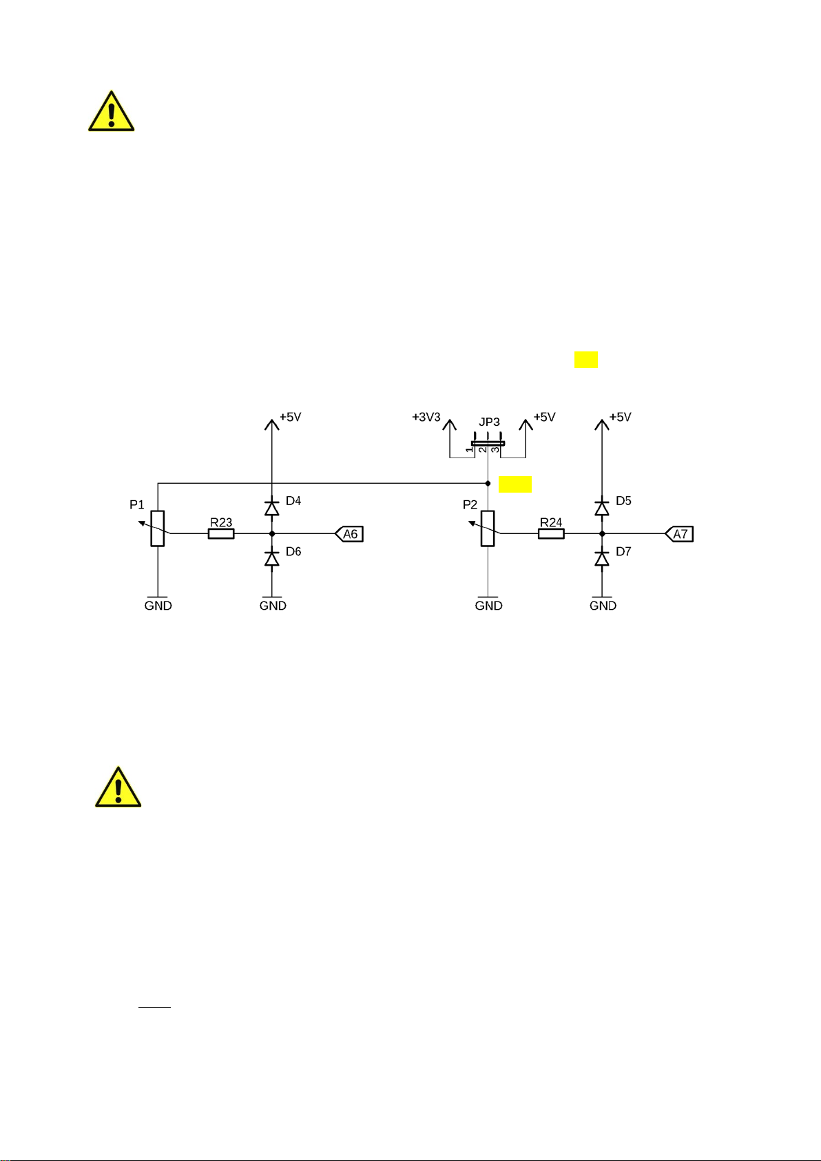
4.5 The potentiometers P1 and P2
The rotary axes of the two potentiometers P1 and P2 at the bottom of Figure 1 (arrow (8) and
arrow (10) in Figure 1) can be used to set voltages in the range 0 … VPot at their wiper con-
nections. The wiring of the two potentiometers can be seen in Figure 6.
Figure 6: The wiring of the potentiometers P1 and P2
The wiper connections of the two potentiometers are connected to the analog inputs A6 and
A7 of the Arduino®NANO microcontroller module via the protective resistors R23 and R24.
The diodes D4, D6 or D5, D7 protect the respective analog input of the microcontroller from
too high or negative voltages.
Caution:
The pins A6 and A7 of the ATmega328P are always analog inputs due to the internal
chip architecture of the microcontroller. Their configuration with the function
pinMode() of the Arduino IDE is not allowed and can lead to incorrect behavior of the
program.
Via the microcontroller’s analog/digital-converter, the set voltage can be measured in a simple
way.
Example for reading the value of potentiometer P1 at connection A6:
int z = analogRead(A6);
The 10-bit numerical value Z, which is calculated from the voltage at A6 according to
Z =
1024⋅
REF
ADC
V
V
(equation 1 from section 5)
is read into the variable z.
UPot
VPot

15
The desired upper limit VPot = +3.3 V resp. VPot = +5 V of the setting range is set with the pin
header JP3 (arrow (9) in Figure 1). To select VPot, either pin 1 or pin 3 of JP3 is connected to
pin2 using a jumper.
Which voltage has to be set with JP3 for VPot depends on the reference voltage VREF of the
analog/digital-converter at the REF connector of the pin header SV6 (arrow (7) in Figure 1),
see section 5.
The reference voltage V
REF of the A/D-
converter at the REF terminal of the SV6
pin header
and the voltage VPot specified with JP3 must match.
4.6 The switches S1 ... S6 and the buttons K1 ... K6
The MCCAB Training Board provides the user with six pushbuttons and six-slide switches for
his exercises (arrows (20) and (19) in Figure 1). Figure 7 shows their wiring.
To give the user the option of applying either a permanent or a pulse signal to one of the
inputs of the microcontroller module M1, one-slide switch and one pushbutton switch are con-
nected in parallel.
The common output of each of the six switch pairs is connected via a protective resistor (R25
... R30) to the pin header JP2 (arrow (21) in Figure 1).
The parallel connection of a slide switch and a pushbutton switch with a common operating
resistor (R31 ... R36) acts like a logical OR operation:
If via one of the two switches (or both switches at the same time) the +5 V voltage is present
at the common working resistor, this logical HIGH level via the protective resistor is also pre-
sent at the corresponding pin 2, 4, 6, 8, 10 or 12 of JP2. Only when both switches are open,
their common connection is open and the corresponding pin of the pin header JP2 is pulled to
LOW level (0 V, GND) via the series connection of the protective resistor and the working
resistor.
Figure 7: The wiring of the slide / pushbutton switches S1 ... S6 / K1 ... K6
Each pin of the pin header JP2 can be connected to its assigned input A0 ... A3, D12 or D13
of the Arduino®NANO microcontroller module via a jumper. The assignment is shown in Figure
7.
Alternatively, a switch connection on pins 2, 4, 6, 8, 10 or 12 of the pin header JP2 can be
connected to any input D2 ... D13 or A0 ... A3 of the Arduino®microcontroller module on the
pin headers SV5 or SV6 (arrow (3) and arrow (7) in Figure 1) using a Dupont cable. This
flexible way of connection is preferable to the fixed assignment of each switch to a specific
GPIO if the assigned GPIO of the ATmega328P microcontroller is used for a special function

16
(A/D-converter input, PWM output ... ). This way the user can connect his switches to the
GPIOs which are free in the respective application, i.e., not occupied by a special function.
In his program, the user has to configure each GPIO of the Arduino®NANO mi-
crocontroller module as
input, which is connected to a switch port, using the in-
struction
pinMode(gpio, INPUT); // for "gpio" insert the corresponding pin number
Example
:
pinMode(
A1, INPUT); // A1 is set up as digital input for S2|K2
In case a GPIO of the microcontroller connected to a switch has been configured as an output
by mistake, the protective resistors R25 ... R30 prevent a short between +5 V and GND (0 V)
when the switch is actuated and the GPIO has LOW level at its output.
To be able
to use a pushbutton switch
, the slide switch connected in parallel
to it must be open (position "0")! Otherwise, their common output is permanently
at HIGH level, regardless of the position of the pushbutton switch.
The switch positions of the slide switches are marked "0" and "1" on the
training board as shown in
Figure 1.
Figure
8 shows: If the switch is in position "1", the switch output is con-
nected to +5 V (HIGH), in position "0" the switch output is open.
Figure 8
4.7 The piezo buzzer Buzzer1
The upper left part of Figure 1 shows Buzzer1 (arrow (23) in Figure 1), which allows the user
to emit tones of different frequencies. Its basic circuitry is shown in Figure 9.
Buzzer1 can be connected to the GPIO D9 of the microcontroller on the MCCAB Training Board
via a jumper on the position "Buzzer" of pin header JP6 (arrow (29) in Figure 1) (see Figure
9, Figure 4 and arrow (2) in Figure 1). The jumper can be removed if the GPIO D9 is needed
in a program for other purposes.
If the jumper is removed, it is also possible to apply an external signal to pin 24 of pin header
JP6 via a Dupont cable and have it output by Buzzer1.
Figure 9: The wiring of Buzzer1
To generate tones, the user must generate a signal in his program that changes with the
desired tone frequency at output D9 of the microcontroller (sketched on the right in Figure 9).
This rapid sequence of HIGH and LOW levels applies a rectangular AC voltage to Buzzer1,
t
T
f =
1
T
+5 V
0 V
Driver
Pin header
i

17
which periodically deforms the ceramic plate inside the buzzer to produce sound vibrations at
the appropriate tone frequency.
An even simpler way to generate a tone is to use T/C1 (Timer/Counter 1) of the microcontrol-
ler:
The T/C1 output OC1A of the AVR microcontroller ATmega328P on the Arduino®NANO micro-
controller module can be connected to GPIO D9 inside the microcontroller chip. With appro-
priate programming of T/C1, it is very easy to generate a rectangle signal whose frequency f
= 1
(T is the period of the rectangle signal) is converted into the desired tone by the buzzer.
Figure 10 shows that a piezo buzzer is not a hi-fi loudspeaker. As can be seen, the frequency
response of a piezo buzzer is anything but linear. The diagram in Figure 10 shows the sound
pressure level (SPL) of the piezo transducer SAST-2155 from Sonitron measured at a distance
of 1 m as a function of the signal frequency. Due to physical properties and natural resonances,
certain frequencies are reproduced louder and others softer. The corresponding diagram of
the piezo buzzer on the MCCAB Training Board shows a similar curve.
Figure 10: Typical frequency response of a piezo buzzer (Image: Sonitron)
Despite this limitation, a piezo buzzer is a good compromise between the reproduction quality
of the sounds generated by the microcontroller and its footprint on the board, which allows it
to be accommodated in a small space.
In cases where a higher quality of sound output is required, the piezo buzzer can be discon-
nected from output D9 by removing the jumper and D9 can be connected to external equip-
ment for sound reproduction on the pin header SV5 e.g., via a Dupont cable (if necessary, via
a voltage divider to reduce the amplitude to avoid damage to the input stage).
4.8 The 3
×
3 LED matrix
The 9 LEDs in the left part of Figure 1 are arranged in a matrix with 3 columns and 3 rows
(arrow (27) in Figure 1). Their circuitry is shown in Figure 11. 9 LEDs can be controlled with
only 6 GPIOs of the microcontroller due to the matrix arrangement.
The three-column lines A, B and C are permanently connected to the pins D8, D7 and D6 of
the microcontroller as shown in Figure 11. The three resistors R5 ... R7 in the column lines
limit the current through the LEDs. In addition, the column lines are connected to the con-
nector SV3 (arrow (25) in Figure 1).

18
The three-row connections 1, 2 and 3 are routed to the pin header JP1 (arrow (28) in Figure
1). They can be connected to the microcontroller’s pins D3 ... D5 by means of jumpers. Alter-
natively, the pins 1, 2 or 3 on header JP1 can be connected via Dupont cables to any output
D2 ... D13 or A0 ... A3 of the Arduino®NANO microcontroller module on both headers SV5
and SV6 (arrow (3) and arrow (7) in Figure 1) if one of the assigned GPIOs D3 ... D5 of the
microcontroller ATmega328P on the Arduino®NANO microcontroller module is used for a spe-
cial function.
The 9 LEDs are labeled A1 ... C3 according to their arrangement within the matrix, e.g., LED
B1 is located at column line B and at row line 1.
Figure 11: The nine LEDs in form of a 3 ×3 matrix
The LEDs are usually controlled by the user program in an endless loop, in which one of the
three rows 1, 2 and 3 is cyclically set to LOW potential, while the other two rows are set to
HIGH level or are in a high-impedance state (Hi-Z). If one or more of the LEDs in the row
currently activated by LOW level is to be lit, its column terminal A, B or C is set to HIGH level.
The column terminals of the LEDs in the active row that are not to be lit are at LOW potential.
For example, to make both LEDs A3 and C3 light up, row 3 must be at LOW level and columns
A and C must be at HIGH level, while column B is at LOW level and both row lines 1 and 2 are
at HIGH level or in high impedance state (Hi-Z).
Caution:
If the row lines of the 3 ×3 LED matrix are either connected to the GPIOs D3 …
D5
via jumpers on the pin header JP1 or to other GPIOs of the microcontroller via
Dupont cables, these row lines as well as the column lines D6 …
D8 must never be
used for other tasks in a program. A double assignment of the matrix GPIOs would
lead to malfunctions or even to damage to the training board!
1
2
3
JP1
A1
B1
C1
C2
B2
A2
A3
B3
C3
A
B
C
SV3
R7
R6
R5
D3
D8
D7
D6
D4
D5

19
4.9 The LC-Display (LCD)
At the top right of Figure 1 is the LC display (LCD) for displaying text or numerical values
(arrow (18) in Figure 1). The LCD has two rows; each row can display 16 characters. Its
circuitry is shown in Figure 12.
The design of the LC display can vary depending on the manufacturer, e.g., white characters
on a blue background or black characters on a yellow background or another appearance is
possible.
Since the LCD is not needed in all programs, the +5 V operating voltage of the LCD can be
interrupted by pulling the jumper on the pin header JP5, if the backlight of the LCD should
interfere.
Figure 12: The connections of the LC display
Contrast setting
The purchaser of the MCCAB Training Board must adjust the contrast of the LC
display during the first start
-up
! To do this, a text is output to the LCD and the
contrast is adjusted by changing the trimming resistor shown in
Figure 13
(white
arrow mark in
Figure 13) with a screwdriver from the bottom of the training board so
that the characters on the display are shown optimally.
If a readjustment is necessary due to temperature fluctuations or aging, the user can
correct the LCD contrast by adjusting this trimming resistor if necessary.
Figure 13: Adjustment of the LCD contrast with a screwdriver
i
+5 V
SCL (A5)
JP5
GND (0 V)
SDA (A4)
Training board
release

20
Transmission of the data to the LC-Display
The LC-Display is controlled via the serial TWI (=I2C) interface of the microcontroller
ATmega328P. Connector A4 on pin header SV6 (arrow (7) in Figure 1) functions as data line
SDA (Serial DAta) and A5 as clock line SCL (Serial CLock).
The LC display on the
MCCAB Training Board normally has the I2C address 0x27.
If another address should be used due to manufacturing reasons, this address is
indicated by a sticker on the display. In the user's sketch, this address must then be
used instead of the address 0x27.
The controller installed on the LC display is compatible with the widely used industrial standard
HD44780, for which there are a large number of Arduino libraries (e.g.,
https://github.com/marcoschwartz/LiquidCrystal_I2C) on the Internet for control via the I2C
bus. The libraries can usually be downloaded free of charge from the respective website.
4.10 The driver outputs SV1 and SV7 for higher output currents
and voltages
The pin headers SV1 (arrow (24) in Figure 1) and SV7 (arrow (17) in Figure 1) can be used
to switch on and off loads that require higher currents than the approx. 40 mA that a normal
microcontroller output can deliver as a maximum. The operating voltage of the external load
can be up to +24 V and the output current can be up to 160 mA. This makes it possible to
control smaller motors (e.g., fan motors), relays or smaller bulbs directly with the microcon-
troller of the training board.
Figure 14 shows the circuit diagram of the two driver outputs.
Figure 14: The driver outputs SV1 and SV7 for higher output currents
The dashed areas in Figure 14 show how loads are connected to the driver output, using the
example of a relay and a motor:
•The positive pole of the external operating voltage is connected to pin 3 (labeled "+" on
the board) of header SV1 resp. SV7. The more positive connection of the load is also con-
nected to pin 3 of the pin header SV1 or SV7.
•The more negative connection of the load is connected to pin 2 (labeled "S" on the board)
of header SV1 resp. SV7.
i
M
K
Table of contents


