elem Energy 2 User manual

11
11
1 ❏❏
❏❏
❏
Index
Soldering point.
Male connector.
Female connector.
M/F faston connector.
Test point.
Supply voltage. Logic supply ground.
Analog supply ground.
Chassis ground.
Earth ground.
Flag joined with one or more flags
GENERALMUSICS.p.A.SalesDivision:47842S.GiovanniinMarignano(RN)ITALY-ViadelleRose,12-tel.0541/959511-fax0541/957404
GENERALMUSIContheNET:http://www.generalmusic.com
TechnicalSpecifications,Introduction,TestProcedures&Adjustments
2
Top&BottomAssemblyViews
5
ResponseCurves
7
8
WiringConnectionsDiagram
9
BlockDiagram
10
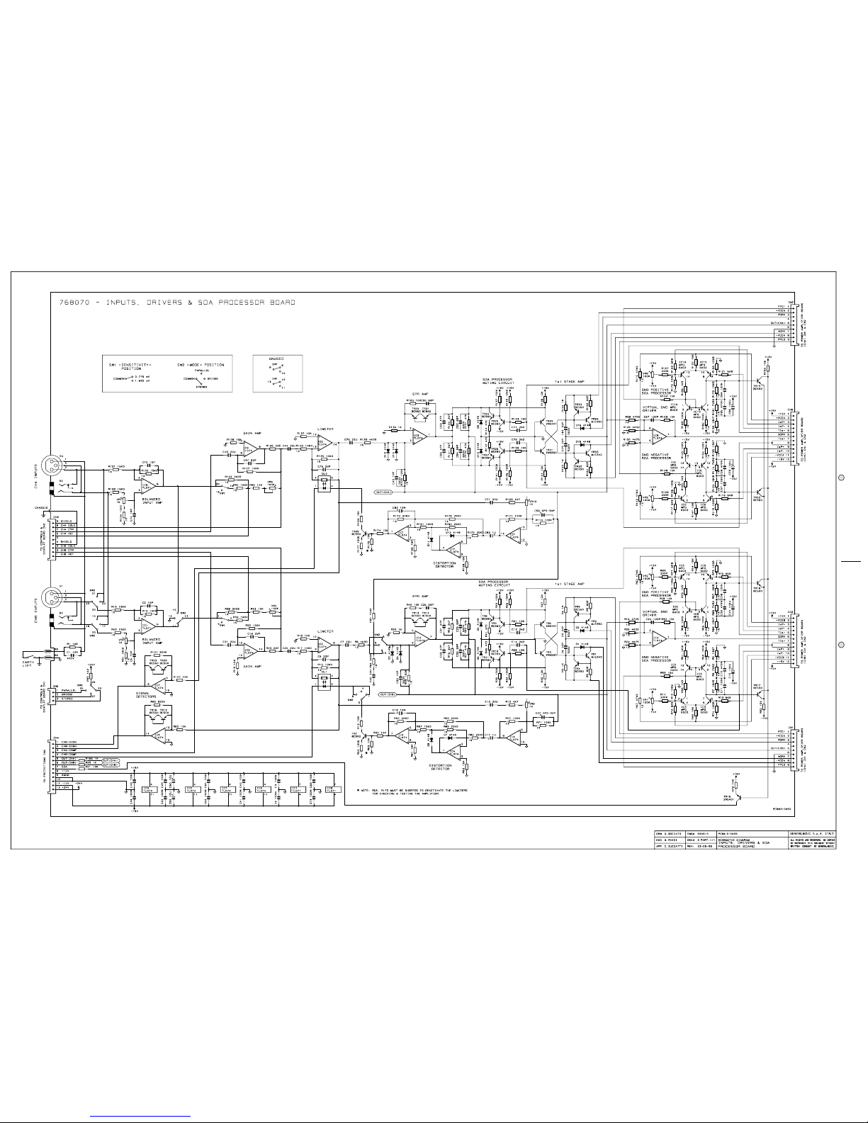
Inputs,Drivers&SOAProcessorBoard
11
SparePartList
12
ProtectionsBoard,Controls&DisplayBoard
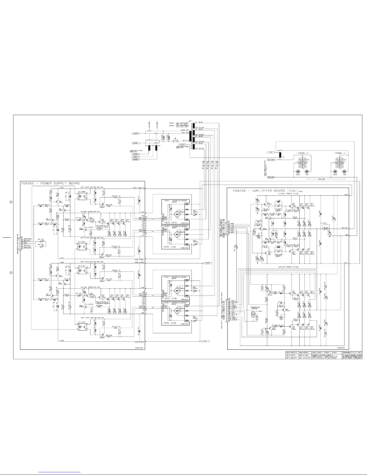
PowerSupplyBoardandAmplifierBoard
6
SERVICE MANUAL
CODE:277287
Warnings
with the same signal name inscribed.
Address
ATTENTION
Observe precautions when handling electrostatic sensitive devices.
Notice
Service must be carried out by qualified personnel only.Any tampering carried out by unqualified personnel during the guarantee period
will forfeit the right to guarantee.
For a correct operation of the instrument, after having switched off, be careful to wait at least 3 seconds before switching on again.
To improve the device's specifications, the schematic diagrams may be subject to change without prior notice.
All components marked by this symbol have special safety characteristics, when replacing any of these components use only
manufacturer's specified parts.
The (µ) micro symbol of capacitance value is substituted by U.
The (
Ω
) omega symbol of resistance value is substituted by E.
The electrolytic capacitors are 25Vdc rated voltage unless otherwise specified.
All resistors are 1/8
Ω
unless otherwise specified.
All switches shown in the "OFF" position. All DC voltages measured to ground with a voltmeter 20KOhm/V.
✔
✔
✔
✔
✔
✔
✔
✔
✔
✔
✔
✔
✔
✔
HIGH PERFORMANCE POWER AMPLIFIER
ENERGY 2

❏ ❏
❏ ❏
❏ 22
22
2
TECHNICAL SPECIFICATIONS
Dimensions: (WxHxD) 483x88x507mm (2U)
Weight: 23 Kg - 50.6 lbs
Power Requirements: 230Vac±10% 50/60Hz 2000VA
or 115Vac±10% 50/60Hz 2000VA
Load selector: * 2Ω ** 4Ω
Output Power: (2Ωstereo/parallel)* 900Watts
(4Ωstereo/parallel)** 1000Watts
(8Ωstereo/parallel)** 500Watts
(4Ωbridge)* 1800Watts
(8Ωbridge)** 2000Watts
(16Ωbridge)** 1000Watts
Max. Undistorted Out: (2Ωstereo/parallel)* 120±2Vpp
(4Ωstereo/parallel)** 180±5Vpp
Input Sensitivity: (constant sensitivity) 0.775Vrms (0dB)
(constant gain) 1.65Vrms (+6.5dB)
Input Impedance: (balanced) 30KΩ
(unbalanced) 15KΩ
Voltage Gain: (constant sensitivity) 38±0.5dB
(constant gain) 32±0.5dB
Slew Rate: 23V/µS
Damping Factor: (8Ωstereo/parallel) >400
Frequency Response (-0.2dB) 20Hz÷20KHz
at Full Power: (-3dB) 10Hz÷80KHz
IMD: (SMPTE 60Hz/7KHz 4:1) <0.02%
THD: (THD+N) <0.02%
S/N Ratio: (unweighted) >100dB
Crosstalk: (1KHz) >90dB
INTRODUCTION
Power Performances
The amplifier Energy 2 operates in AB class using the last BJT generation in
plastic package, it has been designed using a Floating Bridge Configuration: this
configuration, making the most from the double stage power supply, enables to
obtain very consistent power with very high dynamics and low distortion even
at low impedances.
Double Stage Power Supply
For each amplifier section in the Mains Transformer there are two secondary
windings which are connected in parallel or in series according to the effective
power requirements. In this manner the amplifier only receives the necessary
voltage when there is an effective demand of power with a considerable
reduction of dissipated heat.
Protections
Loudspeaker protection: in case of the breakdown of the output BJTs or other
fault condition, a DC Sensor on power output circuit is able to interrupt the
amplifier circuit avoiding that current peaks reach the load. Moreover a Soft
Start circuit delays the connection of the speakers by the Output Relay every
time the amplifier is turned on, when it is turned off the relay disconnect the load
immediately.
Thermal protection and cooling system: Inside the amplifier there is an
highly sophisticated cooling system able to protect it from overheat and to
ensure the upmost efficiency and reliability. The cooling system has two
separate heat sink structures (for positive and negative rails) for each channel
constructed with tinplated copper, instead of alluminium, for more efficiency. Air
flow thru the unit is ensured by two variable speed fans controlled by the SOA
circuit, if the temperature rise again the control circuit gradually reduces the
power supply to the final stage and at the same time enables the input limiter.
As soon as the temperature reaches the normal level , the amplifier gradually
returns to normal operation. The amplifier protect itself, by entering in a
complete muting status, only in extremely abnormal operating condition
(e.g.obstruction of the air vents) and in case of temperature rising further.
SOA processors: In conjunction with the thermal protection the SOA processors
constantly detect the power dissipation of the output BJT ensuring that they
always remain in their Safe Operating Area. In this particular amplifier the SOA
processors are three per channel, the first and most important checks the signal
output stage, the second SOA circuit checks the ground output stage and the
third circuit checks the voltage translator stage, all three circuits operate
accordly.
Current Limiters: These circuits detect the current on final and translator
stages, accordly with SOA processors limiting the excessive current on the
load, and finally enable the Input Limiter.
Transformer Thermal Protection: This protection disconnects the load (muting
the amplifier) until the cooling restores the normal temperature.
Anti-Clipping Limiter: The input signal is constantly checked to instantly
recognize a possible amplifier clip, this circuit is an efficient limiter that operate
without an excessive dynamic compression to obtain the better listening, it
operates accordly the protection circuit.
TEST PROCEDURES & ADJUSTMENTS
Precaution
➭To prevent short circuit during any test, the oscilloscope must be
EARTH insulated, this occurs because some test require to connect its
probe to the amplifier output, non-compliance may cause damages to
oscilloscope inputs circuitry.
➭Before removing or installing any modules and connectors, disconnect
the amplifier from AC MAINS and measure the DC supply voltages
across each of the power suppliy capacitors. If your measurement on any
of the caps is greater than 10Vdc, connect a 100Ω50W resistor across
the applicable caps to discharge them for your safety. Remember to
remove the discharge resistor immediately after discharging caps. Do not
power up the amplifier with the discharge resistor connected.
➭Read these notes entirely before proceeding to any operation. These
notes are not comprehensive of all damages that possibly occur, but
includes some specifically advices, checks and adjustments relative to
this amplifier.
Visual Check
➭Remove top and bottom covers from the amplifier chassis.
➭Use compressed air to clear dust in the amplifier chassis.
➭Before proceed to supply the amplifier check visually the internal assem-
bly, if appears an evident damage find the most possible reasons that
cause it.
➭Check the wiring cables for possible interruptions or shorts.
➭If the damage has burnt a printed circuit board don’t try to repair it,
replace with a new one.
Test Instruments
➭Audio Generator
➭Dual Trace Oscilloscope
➭Digital Multimeter
➭2Ω1000W, 4Ω2000W, 100Ω50W resistors
➭1 Mains cord terminated with insulated Faston
➭Variac (0÷250Vac)
➭Temperature Meter
Initial Setup
➭Turn the amplifier on bottom side.
➭Disconnect the Power Switch from the amplifier internal mains line and
reconnect it directly to the Mains Line with the other cord.
Set the Variac at zero voltage and connect it between the amplifier mains
socket and the Mains Line.
➭Set the amplifier controls as follows:
MODE on parallel (PAR),
MINIMUM LOAD on 4Ω,
EARTH selector on grounds attached,
SENSITIVITY on 0.775V
and turn full clockwise the level potentiometers.
➭Short R63 and R175 on the Inputs, Drivers & SOA Processor Board to
de-activate the limiters on each channel.
➭The procedures that follow must be executed subsequently in the order
specified.
➭The procedures are divided in two phases: the first initial test is intended
to locate the most probably faults, the second final test is intended to
verify and to adjust the amplifier with load connected.
Protections & Ac Supply Check
➭Turn the amplifier on top side.
➭Remove the Main Transformer secondary fuses (4 x16A) and then check
them with the Multimeter.
➭Turn on the amplifier, the relais on the Main Transformer primary winding
must be turn on one a time, the fans go immediately to the max. speed
and after some seconds return to the slow speed, and also the output
relay must turn on. During this time the protect red led lights.
➭If somethings goes different, the amplifier has probably some problem on

33
33
3 ❏❏
❏❏
❏
the Protections Board, first of all check its supplies:
CN4 pin 6 = +24Vdc
CN4 pin 9 = -24Vdc
CN6 pin 8 = +15Vdc
CN6 pin 11 = -15Vdc
➭If the fans don't start or go only to the max. speed, you must check the
Fan Driver circuit (TR1,2,4,6).
If all the circuit is good, you must check on the Inputs, Drivers & SOA
Processor Board the TR16,17,18,19,22 and the SOA Processor circuits
preceding the transistors; to check them quickly disconnect CN3 and CN6
the fan must go only at slower speed.
➭If the Primary Tranformer Relais don't start (also selecting 2Ω or 4Ω
minimum load switch) check their driver circuits, the fault must be prob-
ably in the Transformer Relais Driver circuit on the Protections Board ,
refer to schematics.
➭If the Outputs Relay doesn't start the fault must probably located in the
relay driver or in Soft Start circuit on the Protections Board , refer to
schematics.
➭Turn off the amplifier and check with the multimeter if the SCR on Con-
trolled Bridge Boards are shorted. If one or more are shorted, replace it
with a new one, check also the bridges.
➭Set the oscilloscope CH1 to 10V/div. 5mS and connect its probe to R48
side TR19(c) on Protections Board, turn on the amplifier: a series of
pulses appear on the screen that will became stable about +15Vdc, these
pulses activate the SCR on the Controlled Bridge Boards to slowly charge
the capacitors. If the pulses aren't displayed your amplifier has probably
some fault on Soft Start circuit, refer to schematics.
➭Set the Variac at the nominal mains voltage, measure with the Multimeter
the AC supply voltages between the secondaries: 43±3Vac
➭Switch to 2Ωminimum load and measure again the voltages: 33±3Vac.
➭Re-set the minimum load at 4Ωand the Variac at zero voltage, turn off
the amplifier and put the fuses back on its holders.
Dc Supply Initial Check
➭SETUP:
Connect the audio generator to a channel input and set it to 1KHz
775mVRMS (0dB) sinusoidal signal.
Connect the CH1 scope GND clip to the output GND and connect the
oscilloscope probe tips CH1/2 to the channel outputs before the relay, set
both to DC 20V/div. 200µS/div.
➭Turn on the amplifier and afterwards increase the Variac slowly monitor-
ing the Outputs with the oscilloscope CH1/2 connected, it should display
the sinusoidal input signal amplified with no distortions, if a distortion or a
protection trip occur, turn off the amplifier, wait some minutes and discon-
nect the supplies from the Power Amplifier Board that doesn't work
properly, to do this you must disconnect the red and the blue wires from
capacitors, continue to check the supplies.
➭CAUTION: Before re-connecting the Power Amplifier Boards to the
supplies, you must have the capacitors discharged for your safety:
connect a 100ΩΩ
ΩΩ
Ω50W resistor across the caps and remove the resis-
tor just after they are discharged.
➭Finally verify the DC supplies at the capacitor terminals: 58±2Vdc
➭If one or more voltages don’t correspond:
Check the SCR located on Controlled Bridge Board and its driver transis-
tor (TR9,10,13,14) located on Power Supply Board, particularly check the
insulation from the heating and the driver transistors and the diodes D19,
20, 21, 22.
Re-check the rectifiers, capacitors and transformers disconnecting them
from circuitry, refer to schematics.
Channels Initial Check
➭Re-set the Variac at zero voltage and eventually re-connect the damaged
Power Amplifier Board that you have previously disconnected from
supply.
➭Set up the Variac slowly and check on the oscilloscope display the output
of the damaged channel:
➭If a dc voltage is present, turn off the amplifier and check all the output
transistors TR13, 14, 15, 16, 17, 18, 19, 20, 21, 22, 23, 24, their drivers
TR5, 7, 9, 11 and all active and passive components interested with the
signal path, particularly also include TR29, 30, 31, 32, 33, 34 and D15,
16 for channel A or TR1, 2, 3, 4, 5, 6 and D1, 2 for channel B mounted
on Inputs, Drivers & SOA Processor Board.
➭If appears a simmetrical clipping before the maximum output voltage
(refer to technical spec.), the supply translator circuit of the channel
under test, located on Power Supply Board doesn't work properly: check
its driver circuit refer to schematics.
➭If appears an asimmetrical clipping before the maximum output voltage
(refer to technical spec.), the grounding power amplifier doesn't work
properly; this fault can also be checked measuring the dc voltage be-
tween output ground and the +Vcc and the voltage between output
ground and -Vcc for the channel under test, all measures must be
simmetrical near 28Vdc without input signal, if not, check the virtual
ground driver (R115/R142 ch.A or R52/R47 ch.B) located on Inputs,
Drivers & SOA Processor Board, refer to schematics.
➭If no signal appears: try to disconnect R41,46 to deactivate the signal
deletion caused by SOA circuit, then checked the right operation of the
channel, check the cable connections of SOA circuits, check its active
and passive components and verify its adjustments. If also the signal
doesn't appear check the input circuits, refer to schematics.
➭Note: If one or more of described faults appear only with the load
connected (see the following checks) may be that one or more
output, ground or voltage translator transistors is interrupted.
Dc Supply Final Check
➭These procedures are intended for one channel at a time, repeat these
operation for the other channel.
➭SETUP:
Connect the CH1 scope GND clip to the output GND.
Connect the CH1 probe tip to the CHA amplifier output before the relay.
Connect the CH2 probe tip to the red wire (+Vcc1).
Set both to DC 20V/div. 200µS/div.
Insert the temperature meter through two transistor cases interstice
located at centre of heatsink of CHA on the Power Supply Board .
Connect the 4Ω2000W load to CHA out.
Connect the audio generator to the channel input CHA and set it to 1KHz
775mVRMS (0dB) sinusoidal signal, and set the amplifier to Stereo mode.
Connect the Mains Line as described in the initial setup section.
Set the LEVEL potentiometers at zero.
Set the Variac at zero voltage.
➭Increase slowly the Variac to reach the mains voltage: check that the
supply circuit operate correctly measuring +28±2Vdc on the red wire
(+Vcc1) and -28±2Vdc on the blue wire (-Vcc1) respect the CHA GND
output.
➭Increasing the CHA input level check the right operation of the Supply
Voltage Translator: verifying that the CH2 voltage level remain the same
until the CH1 signal reach 26Vp, afterwards increasing the input level the
voltage of CH1 must envelope externally the CH2 signal with an offset of
10÷12V.
➭Increasing the level of input signal the envelope is stopped more about
100±5Vdc and the signal clip must occur at 180±5Vpp. Decrease the
level and connect the CH2 probe to the blue wire (-Vcc1), repeat the test
for the negative supply.
➭Connect the 2Ωinstead 4Ωload and verify that the output signal must be
limited at 64±2Vp. If it doesn't happen check the limit circuit (TR23 for
CHA, TR24 for CHB) on Power Supply Board.
➭Disconnect the fan and wait until the temperature reaches 110±5°C: the
primary transformer relais switch to 2Ωminimum load and the fan, re-
connecting it, goes at maximum speed (23Vdc).
➭Turn off the Amplifier and the Variac. Connect CH1 scope GND tip to R38
terminal side CN2 (SCR cathode) and its probe tip to R41 side CN2 (SCR
gate), set it to 200mV/div. 1mS/div.
➭Turn on the Amplifier and the Variac simultaneously and verify that the
voltage on the SCR gate shift from 0 to 0.8Vp in less than one second.
➭Repeat the last test after moving the CH1 GND tip to R44 side CN2 and
its probe tip on R46 side CN2 to check the second SCR.
➭Repeat all these tests for CHB, where Vcc1 become Vcc2, CN2, R38,
R41, R44, R46 become CN3, R48, R50, R53, R55 respectively.
Channel Final Check
➭These procedures are intended for one channel at a time, repeat these
operation for the other channel.
➭If you have already repaired the channel under test:
Verify, with the Multimeter, the insulation between the heatsink and the
TR8,10 transistors collectors.
Turn the trimmer VR1 full clockwise and VR2 full counter-clockwise to re-
adjust the Bias current.
➭SETUP:
Connect the scope CH1 and the amplifier as described in Dc Supply Final
Check section.
Connect the CH2 probe tip to the heatsink of the channel under test.
Insert the temperature meter through the PTC R27 (for CHB) or through
the TR15,16 (for CHA) interstice located on the Power Amplifier Board at
centre of heatsink.
Set the LEVEL potentiometers at maximum.
➭INITIAL TEST:
Increase slowly the Variac. The channel output signals must be symmetri-
cal respect the GND without visible distortion and oscillation. If there is a
distortion read the section ADVICES and proceed to check the other
channel.
Increasing the level of input signal the signal clip must occur at 180±
5Vpp.
➭BANDWIDTH CHECK:
Decrease the level to obtain a 50Vp output signal, sweep the generator

❏ ❏
❏ ❏
❏ 44
44
4
frequency from 20Hz to 20KHz, the output level must have not detectable
level changes.
Set back the frequency at 1KHz.
➭BIAS ADJUSTMENT:
Disconnect the fan and wait until the temperature reaches 50°C, set the
input level at zero, measure with the Multimeter the voltage across the
tips of R34 and the tips of R40, adjust VR1 trimmer to read 1±0.05mVdc.
Verify that the temperature is not changed and adjust VR2 trimmer to
read 1±0.05mVdc across the tips of R30 and the tips of R43.
Set the CH1 an CH2 scopes at 0.2V/div. 200µS/div., adjust the input level
until the sinewave reach 0.5Vp, no crossover distortion must be detect-
able: if necessary re-adjust VR2 until the distortion disappears without
exceed 6mVdc between R30 and R43 terminals.
Re-connect the fan.
➭OUTPUT CURRENT CHECK (GROUND AMPLIFIER):
Connect the ground clip of CH1 scope at the CHA amplifier ground out,
and its probe tip to the emitter of TR16 and CH2 probe tip to TR21 emit-
ter.
Vary the input level to obtain 0.5Vp on output and verify that the differ-
ence of their peaks are less than 0.1V.
Verify the correct division of the output current between the output tran-
sistor, connecting alternatively CH2 probe tip to the TR17 and TR18
emitters checking that their peak levels are within 10% themselves.
Moving the CH1 probe tip on TR21 emitter, repeat the measure with the
CH2 tip connected alternatively to TR19 and TR20 emitters.
➭OUTPUT CURRENT CHECK (SIGNAL AMPLIFIER):
Connect the ground clip of CH1 scope at the CHA amplifier output, and
its probe tip to the emitter of TR13 and CH2 probe tip to TR24 emitter.
Vary the input level to obtain 0.5Vp on output and verify that the differ-
ence of their peaks are less than 0.1V.
Verify the correct division of the output current between the output tran-
sistor, connecting alternatively CH2 probe tip to the TR14 and TR15
emitters checking that their peak levels are within 10% themselves.
Moving the CH1 probe tip on TR24 emitter, repeat the measure with the
CH2 tip connected alternatively to TR22 and TR23 emitters.
➭SHORT CIRCUIT SENSOR CHECK:
Short the load temporarely and verify that the current protection sensor
(TR3, TR4) limits simmetrically the signal at 0.8±0.1Vp.
Input Circuit Check
➭These procedures are intended for one channel at a time, repeat these
operation for the other channel.
➭SIGNAL/CLIP SENSOR CHECK:
Set the LEVEL pot to minimum, then increase the level and check the
SIGNAL/CLIP led activity: it must turn on (green light) when the amplifier
output is higher than 0.5Vp.
➭CMRR ADJUSTMENT:
Temporarily disconnect pin 3 from pin 1 and short the pin 2 (positive
input) and pin 3 (negative input) of XLR or Jack plug.
Adjust the trimmer VR7 (CHA) or VR4 (CHB) on Inputs, Drivers & SOA
Processor Board to obtain the minimum output level. Re-set the genera-
tor plug with the input signal at pin 2 (positive input) and pin 3 (negative
input) short with pin 1 (GND).
➭GAIN ADJUSTMENT:
Set the input signal to 0dB. Connect the Multimeter on the output of the
channel under test, set it in dB scale if available, set the input SENSITIV-
ITY at 1.65VRMS, adjust the trimmer VR6 (CHA) or VR5 (CHB) to obtain
32dB (30.8VRMS) on the output.
Set the SENSITIVITY to 0.775VRMS and verify that the Multimeter show
38.5 dB (84.1VRMS).
➭LIMITER ADJUSTMENT:
Remove the shorts from R175 (CHA) and from R63 (CHB) on Inputs,
Drivers & SOA Processor Board, connect CH2 probe tip to IC7 pin 14
(CHA) or to IC4 pin 8 (CHB) and set it at 5V/div. 2mS/div., change the
generator frequency to 100Hz, increase the signal to obtain about 40Vp
on output and adjust the VR10 (CHA) or VR3 (CHB) for the minimum
signal on CH2 trace without CH1 trace attenuation.
Change the frequency to 10KHz and adjust the C56 (CHA) or C37 (CHB)
to minimize the signal on CH2 scope without CH1 attenuation.
Re-set the generator at 1KHz, increase the signal and verify that the
clipping remain costant with the limiter intervention indicated by the red
colour of the SIGNAL/CLIP led.
➭SOA ADJUSTMENT:
Set the scope sensitivity at 5V/div. (both channels).
Connect the CH1 GND clip to S6 and its probe tip to IC6 (CHA) or IC3
(CHB) pin 8, connect CH2 probe tip to IC10 (CHA) or IC5 (CHB) pin 8 set
both at 5V/div. 200µs/div..
Insert the temperature meter through the PTC R27 (for CHB) or through
the TR15,16 (for CHA) interstice located on the Power Amplifier Board at
the centre of heatsink.
Verify that the two scope traces are located about 11±0.5Vdc.
Short temporarely the load, verify that both the traces move to the scope
screen centre and the fans turn to maximum speed.
Disconnect the fan and leave the temperature increasing until reaches
70°C disconnect the load and adjust:
VR8 (CHA) VR2 (CHB) to have the scope negative trace at 10.5Vdc.
VR9 (CHA) VR1 (CHB) to have the scope positive trace at 11.5Vdc.
Short again the load, verify that the scope traces move more about 2V
from the screen centre when the temperature reach 100±5°C; re-active
the fans, they would go at the max. speed, decrease the input level at
zero and verify that the voltage remains at 28±2V until the temperature
reaches 85±2°C on the heatsink, then change the load back to 4Ω.
➭AMPLIFIER BRIDGE MODE CHECK:
Set the amplifier in BRIDGE mode (input signal to channel A) and MINI-
MUM LOAD at 2Ω, connect the CH2 probe to the bridge output: the
output voltage must be 120±2Vp.
➭SIGNAL TO NOISE RATIO CHECK:
Disconnect the audio generator and short the input (pin 1,2,3 of XLR plug
shorted) the output signal (noise) must be less 1mV.
➭OFFSET SENSOR CHECK:
Set the Variac to zero voltage output, disconnect the load. Turn on the
amplifier, connect temporarily (by means of a suitable 100KΩresistor
with a conductor wire) the positive terminal of C4 (CHA) or C5 (CHB) to
+15Vdc supply (CN6 pin 8): the PROTECT led must turn on in 3 seconds
approx., the output relay must switch off.
Remove the connection, wait until the leds turn off and after some sec-
onds repeat the check with -15Vdc supply (available on CN6 pin 11), the
led PROTECT must turn on again.
➭SLEW RATE CHECK:
Set the scope sensitivity to 10V/div. 1µS/div. and set the generator to
1KHz square wave mode. Check the output square wave rising and falling
edge slopes: both must be 20V/µS or more.
Advices
➭Check the channels one at time to determine which is right (note: if you
have a spare amplifier module that you know as right, use it).
➭If you have determinate that the problem is a short on a rail, you must
check the output transistors.
To determine which transistor devices are bad, use a soldering iron to lift
one leg of each emitter pin and measure the emitter-collector resistance
on each device. Unsolder and lift one leg of each base pin and check the
base-collector resistance of each transistor and replace any that measure
as a short.
➭If all the transistors are OK, unsolder and lift one leg of each diode and
check them.
➭Check the circuit board for open foil traces.
➭Use the Multimeter as Ohm-meter to check the resistors, particularly the
base and emitter resistors of damaged transistor.
➭Check all active components (transistor and diodes) on the signal path
before a faulted component.
➭Check all active components (transistor and diodes) connected to the
output net when a output transistor has been faulting.
➭If the input sinewave appears to be distorted during the negative cycle,
you can assume that the problem is located somewhere in the circuitry of
the positive rail.
If the positive cycle appears distorted, you can assume that the problem
is in the circuitry of the negative rail. Refer to the schematics.
Transistor Packages
TO92
BC337, BC550, BC560
1=Collector
2=Base
3=Emitter
2N5550, 2N5401
1=Emitter
2=Base
3=Collector
TO126
MJE340, MJE350, MJE802
1=Emitter
2=Collector
3=Base
TO220
TIP127, MJE15030, MJE15031
1=Base
2=Collector
3=Emitter
4=Collector TO264
MJE21193, MJE21194
1=Base
2=Collector
3=Emitter
BTW69
1=Kathode
2=Anode
3=Gate
55
55
5 ❏❏
❏❏
❏
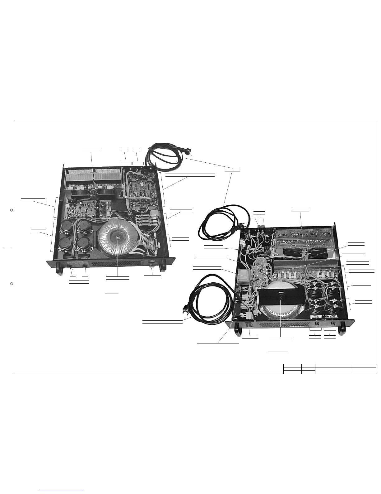
GENERALMUSIC S.p.A. Italy
SCHEMATIC DIAGRAM ENERGY 2
TOP & BOTTOM VIEWS
DRW: BOCCATO
APP: REV: 19-05-98
DISK: PART: 1/1CKD:
ALL RIGHTS ARE RESERVED, NO COPIES OR
REPRODUCE THIS DOCUMENT WITHOUT
WRITTEN CONSENT BY GENERALMUSIC.
TOP VIEW
CHA AMPLIFIER
BOTTOM VIEW
DWG:
CHA CHB
INPUTS, DRIVERS & SOA PROCESSORS BOARD
SECONDARY FUSES
PRIMARY FUSE
MAINS SWITCH
MAIN TRANSFORMER
CHA CHB
LEVEL CONTROLS
CAPACITORS
PROTECTIONS BOARD
MAINS CORD
OUTPUTS
CHACHB
CHB AMPLIFIER
COOLER FANS
POWER SUPPLY CHB
POWER SUPPLY CHA
POWER SUPPLY BOARD
NEGATIVE CAPs
POSITIVE CAPs
CHB CAPsCHA CAPs
MAIN TRANSFORMER
MAINS SWITCH
2
Ω
/4
Ω
PRIMARY TRANSFORMER RELAIS
SERVICES TRANSFORMER
CONTROLLED BRIDGE BOARDS
OUTPUTS RELAY
2ND MAINS CORD (FOR SERVICE ONLY)

❏ ❏
❏ ❏
❏ 66
66
6
GENERALMUSIC S.p.A. Italy
SCHEMATIC DIAGRAM ENERGY 2
MEASUREMENT
DRW: BOCCATO
APP: REV: 19-05-98
DISK: PART: 1/1CKD:
ALL RIGHTS ARE RESERVED, NO COPIES OR
REPRODUCE THIS DOCUMENT WITHOUT
WRITTEN CONSENT BY GENERALMUSIC.
DWG:
Frequency Response
STEREO configuration
Both channels
Input level: 0dB
Load Impedance: 8Ω
Output Power: 5W
Frequency Response
STEREO configuration
Both channels
Input level: 0dB
Load Impedance: 8Ω
Output Power: 500W
Distortion (THD+Noise) vs Frequency
STEREO configuration
Both channels
Input level: 0dB
Load Impedance: 8Ω
Output Power: 500W
Distortion (THD+Noise) vs Output Power
STEREO configuration
Both channels
Input level: 0dB
Load Impedance: 8Ω
Crosstalk
STEREO configuration
Both channels
Input level: 0dB
Load Impedance: 8Ω
Output Power: 500W
Signal to Noise Ratio
STEREO configuration
Both channels
Input level: 0dB
Load Impedance: 8Ω
Damping Factor
STEREO configuration
Both channels
Input level: 0dB
Load Impedance: 8Ω
Output Power: 500W
CMRR
STEREO configuration
Both channels
Input level: 0dB
Load Impedance: 8Ω
GENERALMUSIC - AMPRESP &vs
-4.000
-3.500
-3.000
-2.500
-2.000
-1.500
-1.000
-.5000
0.0
.50000
1.0000
AMPL(dBr)
-50.0
-40.0
-30.0
-20.0
-10.0
0.0
10.00
20.00
30.00
40.00
50.00
PHASE(deg)
10 100 1k 10k 50k
FREQ(Hz)
GENERALMUSIC - AMPRESP &vs
-4.000
-3.500
-3.000
-2.500
-2.000
-1.500
-1.000
-.5000
0.0
.50000
1.0000
AMPL(dBr)
-50.0
-40.0
-30.0
-20.0
-10.0
0.0
10.00
20.00
30.00
40.00
50.00
PHASE(deg)
10 100 1k 10k 50k
FREQ(Hz)
GENERALMUSIC - THD-FREQ vs
0.005
0.010
0.1
1
THD+N(%)
10 100 1k 10k 50k
FREQ(Hz)
GENERALMUSIC - CROSSTLK vs
-140.0
-130.0
-120.0
-110.0
-100.0
-90.00
-80.00
-70.00
-60.00
-50.00
-40.00
-30.00
-20.00
-10.00
0.0
BANDPASS(dBr)
10 100 1k 10k 50k
FREQ(Hz)
GENERALMUSIC - NOISE vs
-140.0
-120.0
-100.0
-80.00
-60.00
-40.00
-20.00
0.0
BANDPASS(dBr)
10 100 1k 10k 50k
FREQ(Hz)
GENERALMUSIC - DAMPING vs
10
100
1k
RLOAD/R0(%)
10 100 1k 10k 50k
FREQ(Hz)
GENERALMUSIC - CMRR vs
-140.0
-130.0
-120.0
-110.0
-100.0
-90.00
-80.00
-70.00
-60.00
-50.00
-40.00
-30.00
-20.00
-10.00
0.0
BANDPASS(dBr)
10 100 1k 10k 50k
FREQ(Hz)
GENERALMUSIC - THD-PWR vs
0.005
0.010
0.1
1
THD+N(%)
110 100 1k
AMPL(W)
20KHz
1KHz
20Hz

77
77
7 ❏❏
❏❏
❏

❏ ❏
❏ ❏
❏ 88
88
8

99
99
9 ❏❏
❏❏
❏
❏ ❏
❏ ❏
❏ 1010
1010
10
1111
1111
11 ❏❏
❏❏
❏

❏ ❏
❏ ❏
❏ 1212
1212
12
Spare Part List
abbreviation explanation
(EU) = specify Europe version
(US) = specify U.S. version
Code Description
Accessories
277286 Owner's Manual
Assembly
778072 Mains & Outs Cables Assembly
778071 Cables Assembly
778048 Supply Cables Assembly
667671 Filter Front Panel
667624 Rear Panel
667623 Front Panel
667542 Bottom Cover
667541 Top Cover
667539 Chassis
657232 Level Knob
340186 Adhesive Cable Fixing
238072 Main Transformer 230Vac 2100W (EU)
238073 Main Transformer 115Vac 2100W (US)
237060 Service Transformer 230Vac 60W (EU)
237061 Service Transformer 115Vac 60W (US)
210249 Air Foam Filter
210216 Adhesive Rubber Foam 20x5mm (Specify mt)
210215 Adhesive Rubber Foam 10x1.9mm (Specify mt)
190224 Lateroid Air Redirector
190222 Lateroid Cover
177542 Handle
130285 Mains Cable (EU) (US)
110317 Relay 24V / 1 Switch no 30A 250V
110291 Power Switch
110120 Fuse Clip 6,3x32mm
110115 Fuse Clip 5x20mm
110038 T15A Fuse 6.3x32mm (US)
110004 T400mA Fuse 5x20mm (EU)
030895 22000u 20% 63V Electrolytic Capacitor
Controls & Display Board
768035 Controls & Display Board (Pcb#319045)
141060 * 12 Contacts Vert Male Connector
141059 * 9 Contacts Vert Male Connector
080734 * Led 2.5x5mm Rect Diff Red-Grn
080732 * Led 2.5x5mm Rect Diff Yellow
080731 * Led 2.5x5mm Rect Diff Red
074570 * 5K 31steps Linear Potentiometer
Protections Board
768077 Protections Board (Pcb#319024)
141060 * 12 Contacts Vert Male Connector
141059 * 9 Contacts Vert Male Connector
141058 * 6 Contacts Vert Male Connector
141056 * 3 Contacts Vert Male Connector
140068 * 3 Contacts Terminal Block
110305 * Relay 12V / 2 Switch 1A 250V
110119 * Fuse Clip 10A max (EU) (US)
110012 * T1.6A Fuse 5x20mm (EU)
100929 * TLP521-2 Dual Optocoupler
100921 * LM339 Quad Voltage Comparator
100060 * 7815 +15V 1A Voltage Regulator
100049 * 7915 -15V 1A Voltage Regulator
090920 * MJE802 TO126 Npn Darl Transistor
090558 * TIP127 TO220 Pnp Darlington Transistor
090200 * 2N5550 TO92 Npn Transistor
090194 * BC560 TO92 LN Pnp Transistor
090183 * BC550 TO92 LN Npn Transistor
090152 * BC337 TO92 Npn Transistor
080302 * 20V 1W 5% Zener Diode
080293 * 15V 1W 5% Zener Diode
080168 * W02M 1.5A Rectifier Diodes Bridge
080156 * 1N4002 1A 100V Rectifier Diode
080103 * 1N4148 100mA 75V Signal Diode
Inputs, Drivers & SOA Processor Board
768070 Inputs, Drivers & SOA Processor Board (Pcb#319059)
757942 * Manufacturer Analog Optoisolator
141184 * Hor Female XLR Socket (NC3FPRH Neutrik)
141060 * 12 Contacts Vert Male Connector
141059 * 9 Contacts Vert Male Connector
141056 * 3 Contacts Vert Male Connector
140220 * Jack Slim H F APJ678 Adimpex Socket
110299 * 4sw 2pos Horizontal Slider Switch
110255 * 6sw 3pos Vertical Slider Switch
100937 * MPQ6002 Quad Compl Pair Trans
100084 * TL074 Quad J-Fet Operational Amplifier
100019 * TL071 LN J-Fet Operational Amplifier
090917 * MJE350 TO126 Pnp Transistor
090916 * MJE340 TO126 Npn Transistor
090201 * 2N5401 TO92 Pnp Transistor
090200 * 2N5550 TO92 Npn Transistor
090194 * BC560 TO92 LN Pnp Transistor
090183 * BC550 TO92 LN Npn Transistor
080103 * 1N4148 100mA 75V Signal Diode
070241 * 100K 20% Horizontal Linear Trimmer
070121 * 1K 20% Horizontal Linear Trimmer
042725 * 100K 1/4W 1% Metalized Film Resistor
042685 * 47K5 1/4W 1% Metalized Film Resistor
042634 * 20K0 1/4W 1% Metalized Film Resistor
042628 * 16K5 1/4W 1% Metalized Film Resistor
042625 * 15K0 1/4W 1% Metalized Film Resistor
042616 * 13K7 1/4W 1% Metalized Film Resistor
042605 * 10K0 1/4W 1% Metalized Film Resistor
042586 * 7K50 1/4W 1% Metalized Film Resistor
042565 * 4K99 1/4W 1% Metalized Film Resistor
042564 * 4K75 1/4W 1% Metalized Film Resistor
042557 * 4K32 1/4W 1% Metalized Film Resistor
042515 * 2K05 1/4W 1% Metalized Film Resistor
042513 * 1K82 1/4W 1% Metalized Film Resistor
042485 * 1K00 1/4W 1% Metalized Film Resistor
010602 * 5p2-30pF N750 Ceramic Capacitor Trimmer
Controlled Bridge Assembly
727551 Quad Controlled Bridge Assembly (Pcb#319041 x4)
340078 * TO220 Insulated Bush
177587 * Heatsink
141061 * 3 Contacts Hor Male Connector
120857 * Vertical Male Faston 6.3mm
080608 * 36MB20A 35A 200V Rectifier Diode Bridge
080553 * BTW69 40A 200V TO3 Scr Diode
Power Supply Assembly
727547 Power Supply Assembly
768069 * Power Supply Board (Pcb#319054)
778074 ** Supply Cables Assembly
141059 ** 9 Contacts Vert Male Connector
141058 ** 6 Contacts Vert Male Connector
100929 ** TLP521-2 Dual Optocoupler
090201 ** 2N5401 TO92 Pnp Transistor
090200 ** 2N5550 TO92 Npn Transistor
090194 ** BC560 TO92 LN Pnp Transistor
080293 ** 15V 1W 5% Zener Diode
080158 ** 1N4006 1A 800V Rectifier Diode
080103 ** 1N4148 100mA 75V Signal Diode
060591 ** 8K2 2W 10% Resistor
060560 ** 4K7 1W 5% Resistor
060034 ** 0E15 5W 5% Wire Resistor
667545 * Heatsink
558006 * Quadruple MJL21194 Selection
090924 ** MJL21194 TO264 Npn Transistor
340079 * TO220 Mica Washer
340078 * TO220 Insulated Bush
090918 * MJE15030 TO220 Npn Transistor
090917 * MJE350 TO126 Pnp Transistor
090916 * MJE340 TO126 Npn Transistor
080821 * Ptc 90 PTH59F04BE222TS
080172 * MUR1510 15A 100V Ultrafast Recovery Diode
Amplifiers Assembly
737065 Dual Amplifiers Assembly with Fans
727548 * Fan Assembly
141055 ** Female Crimping Contact
141050 ** 3 Contacts Female Connector Housing
110363 ** 24Vdc (80x32cm) Fan
727546 * Amplifier Assembly
768068 ** Amplifier Board (Pcb#319053)
778073 *** Amplifier Cables Assembly
230578 *** 2u7H Vert Coil For Amplifier
230530 *** 1uh 10% 630ma Rf Coil
141065 *** 12 Contacts Hor Male Connector
141063 *** 6 Contacts Hor Male Connector
090194 *** BC560 TO92 LN Pnp Transistor
090183 *** BC550 TO92 LN Npn Transistor
080158 *** 1N4006 1A 800V Rectifier Diode
080156 *** 1N4002 1A 100V Rectifier Diode
080103 *** 1N4148 100mA 75V Signal Diode
070106 *** 470E 20% Horizontal Linear Trimmer
060174 *** 2E7 5W 10% Wire Resistor
060171 *** 2E2 2W 10% Resistor
042345 *** 75E0 1/4W 1% Metalized Film Resistor
667543 ** Heatsink
558005 ** Triple Selected Kit of MJL21194
090924 *** MJL21194 TO264 Npn Transistor
558004 ** Triple Selected Kit of MJL21193
090923 *** MJL21193 TO264 Pnp Transistor
340750 ** TO126 Mica Washer
340079 ** TO220 Mica Washer
340078 ** TO220 Insulated Bush
190225 ** Lateroid Air Redirector
100925 ** LM334 Adjustable Current Source TO92
090920 ** MJE802 TO126 Npn Darl Transistor
090919 ** MJE15031 TO220 Pnp Transistor
090918 ** MJE15030 TO220 Npn Transistor
090917 ** MJE350 TO126 Pnp Transistor
090916 ** MJE340 TO126 Npn Transistor
080821 ** Ptc 90 PTH59F04BE222TS
190223 * Lateroid Protection
Note:
Each spare part is single quantity unless otherwise specified.
Asterisk prefix explanation:
Omitted = First level spare part.
One asterisk = Second level, part of previous listed first level part.
Two asterisk = Third level, part of previous listed second level part.
Three asterisk = ............
Any request for not above mentioned part must encompass specific description including:
1) Model name,
2) Section name,
3) Module code,
4) Reference name,
5) Quantity number.
Table of contents


