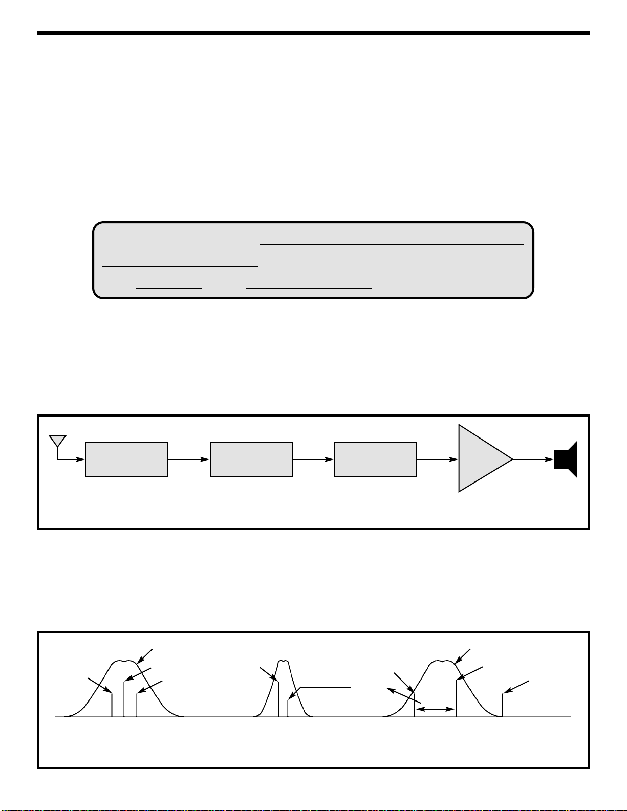
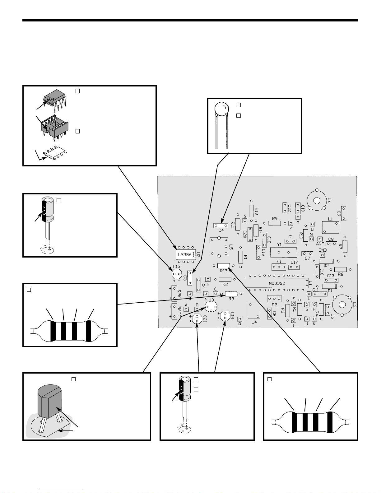
PARTS LIST
If you are a student, and any parts are missing or damaged, please see instructor or bookstore. If you purchased this FM
receiver kit from a distributor, catalog, etc., please contact ElencoTM Electronics (address/phone/e-mail is at the back of this
manual) for additional assistance, if needed.
RESISTORS
Qty. Symbol Value Color Code Part #
1R9 0ΩJumper Wire (use a discarded resistor lead)
1 R15 10Ω5% 1/4W brown-black-black-gold 121000
2 R10, R12 1kΩ5% 1/4W brown-black-red-gold 141000
2 R3, R7 3.3kΩ5% 1/4W orange-orange-red-gold 143300
2 R4, R6 4.7kΩ5% 1/4W yellow-violet-red-gold 144700
1 R8 8.2kΩ5% 1/4W gray-red-red-gold 148200
1 R11 10kΩ5% 1/4W brown-black-orange-gold 151000
1 R5 20kΩ5% 1/4W red-black-orange-gold 152000
1 R2 47kΩ5% 1/4W yellow-violet-orange-gold 154700
1 R1 68kΩ5% 1/4W blue-gray-orange-gold 156800
1 VR2 5kΩ20% linear 192450
2 VR1, VR3 100kΩknurl shaft 192614
-1-
Qty. Symbol Value Marking Part #
1 C5 3.9pF Discap 3.9 203921
1 C8 7pF 20% 25V 7 207000
1 C6 33pF 10% 50V Disc 33 213317
1 C6A 39pF 39 213917
1 C17 51pF 10% 51K 215110
1 C12 68pF 10% 68K 216816
1 C1 120pF 121 221280
1 C7 470pF 10% 50V Disc 471 224717
Qty. Symbol Value Marking Part #
1 C10 1000pF 10% 50V 102 231035
1 C2 .005µF 20% 25V 502 or .005 235025
3 C11,C13,C16 .01µF +80, –20% 103 241031
1 C22 .047µF +80, –20% 50V 473 244780
6 C3,C4,C9 .1µF +80, –20% 50V 104 251010
C18,C19,C20
2 C14, C21 4.7µF 50V Radial 4.7µF 50V 264747
1 C15 220µF 16V Radial 220µF 16V 282244
SEMICONDUCTORS
Qty. Symbol Value Marking Part #
2 D1, D2 Diode 1N914 1N914 310914
1 U2 IC LM386N-1 Audio Amp LM386N-1 330386
1 U1 IC MC3362P FM Receiver MC3362P 333362
1 U3 IC 78L05 Regulator +5V 78L05 338L05
Qty. Symbol Value Part #
1 L4 Coil (1.5 turns coated wire) 430170
1 L1 Coil (4.5 turns coated wire) 430180
1 L5 Coil (metal can yellow) 430260
2 L2, L3 Coil (on form with core) 468752
MISCELLANEOUS
Qty. Symbol Description Part #
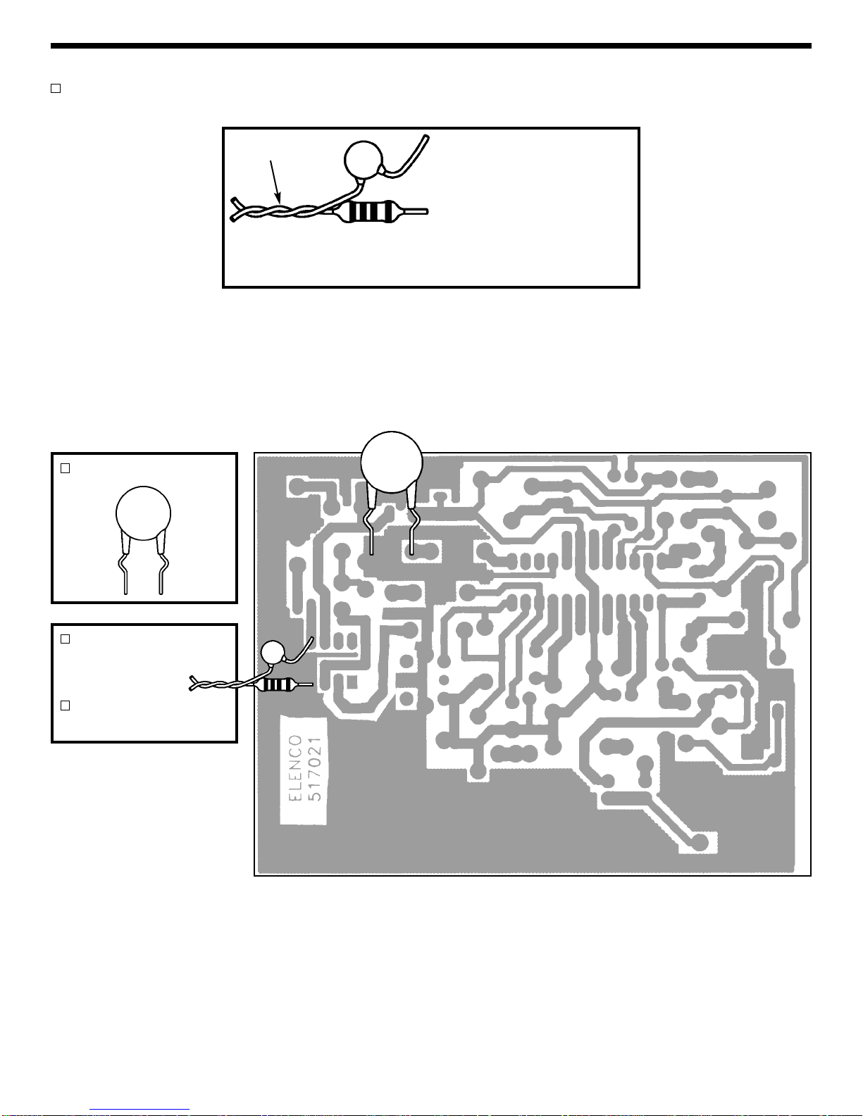
1 PC Board 517021
2 SW1, SW2 Switch Slide DPDT 541021
1 F2 Filter Ceramic 10.7MHz 560107
1 F1 Filter Ceramic 455kHz 560455
1 Y1 Crystal 10.245MHz 561024
1 Battery Snap 9V 590098
1 Battery Holder 9V 590099
1 SPK Speaker 8Ω590102
3 Bracket L-shaped 613000
1 Front Panel 614107
4 Nylon Clips 621012
1 Phono Plug 621017
2 Knob Push-on 622009
1 Knob Large 622080
1 Phono Jack 622103
1 Case Plastic 623240
Qty. Symbol Description Part #
1 Alignment Tool 629011
4 Screw 2-56 x 1/4” 641237
3 Screw 4-40 x 1/4” 641433
3 Nut 7mm Hex 644101
4 Nut 2-56 Hex 644201
3 Nut 4-40 Hex 644400
3 Flat Washer 645101
3 Lock Washer 5/16” internal tooth 646101
3 Lock Washer #4 internal tooth 646401
1 IC Socket 8-pin 664008
1 IC Socket 24-pin narrow 664025
1 Tape Double-sided Foam 740004
1 Wire #22 Solid Orange 84” 814320
1 Cable Shielded 2-conductor 876090
1 Solder Tube 9ST4