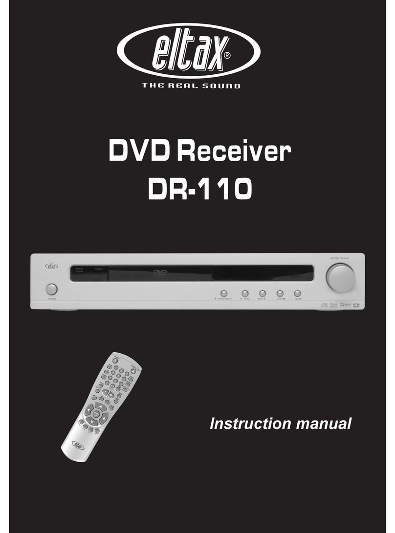
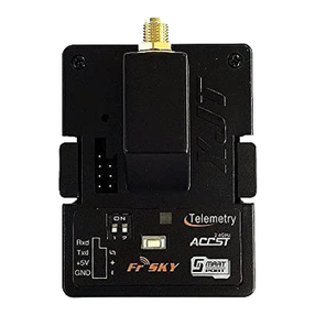
Eltax AVR-800 User manual

6.1 Channel
Home Theatre Receiver
SERVICE MANUAL
AVR-800
CONTENTS
Specifications .......................................................... 2
Measurements And Adjustments ............................ 3
Troubleshooting....................................................... 5
IC Internal Diagrams ............................................... 6
Electrical Parts List................................................ 27
Block Diagram ....................................................... 33
Wiring Diagram...................................................... 35
Schematic Diagrams ............................................. 37
Printed Circuit Boards ........................................... 45
Exploded View....................................................... 53

- 2 -
SPECIFICATIONS
Amplifier Section
Output Power
Stereo Mode : 120W/CH
(1% THD 1KHz 8ohm DIN)
Surround Mode : 92W/CH
(1% THD 1KHz 8ohm DIN)
THD : 0.01%
DOLBY DIGITAL Mode:
Surround : 0 ~ 15 ms
Center : 0 ~ 5 ms
Back surround : 0 ~ 20 ms
DOLBY PRO LOGIC Mode (Surround):
Music : 0~5 ms
Movie : 10~25 ms
Emulation : 10~25 ms
Frequency Response:
*LINE: 10 Hz – 70 kHz, +1/ –3 dB
Signal-to-Noise Ratio:
*LINE: 100dB (IHF-A)
Tone Control:
BASS: ± 10 dB at 100 Hz
TREBLE: ± 10 dB at 10 kHz
Digital Audio Section
Sampling Frequency: 32 kHz, 44.1 kHz, 48 kHz, 96 kHz
DIGITAL Input Level/Impedance:
DIGITAL 1, 2 (OPTICAL): –15 dBm — –21 dBm
DIGITAL 3 (COAXIAL): 0.5 Vp-p / 75 ohms
FM Tuner Section
(Without notes 100.1 MHz, 65 dBf)
Tuning Range:
87.5 MHz – 108.0 MHz (50 kHz steps)
Usable Sensitivity (IHF):
Mono: 11.2 dBf
50 dB Quieting Sensitivity:
Mono: 15.3 dBf
Stereo: 38.5 dBf
Capture Ratio: 2.0 dB
Image Rejection Ratio: 45 dB
AM Suppression Ratio: 55 dB
Total Harmonic Distortion (1 kHz):
Mono: 0.2%
Stereo: 0.3%
Frequency Response: 30 Hz – 15 kHz, +1/ –1.5 dB
Stereo Separation (1 kHz): 40 dB
Signal-to-Noise Ratio:
Mono: 70 dB
Stereo: 65 dB
AM Tuner Section
Tuning Range:
522 kHz – 1,620 kHz (9 kHz steps)
Usable Sensitivity: 55 dB/m
Total Harmonic Distortion: 0.8% at 85 dB/m
Signal-to-Noise Ratio: 45 dB at 85 dB/m
Video Section
Input Sensitivity/Impedance: 1.0 Vp-p/75 ohms
Output Level/Impedance: 1.0 Vp-p/75 ohms
General
Power Requirements:
230 V AC, 50 Hz
Power Consumption:
320W
AC Outlets:
Switched x 1, 100 W max.
Dimensions (W x H x D)
435 x 165 x 350 mm (17-1/8" x 6-1/2" x 13-3/4")
Weight (net):12Kg
*LINE means CD, TAPE, VCR/VID 1, TV/VID 2, AUX/VID 3 and
DVD/CD.
<Improvements may result in specifications and features
changing without notice.
<Illustrations may differ slightly from production models.

Item
Band
AM30%400Hz
FM100%(40KHz Dev.)400Hz
TUNER MODULE
ModulationModulation frequency
- 3 -
MEASUREMENTS AND ADJUSTMENTS
ALIGNMENT INSTRUCTIONS
EQUIPMENT NEEDED
AM Signal Generator
FM Signal Generator
Oscilloscope
VTVM(AC,DC)
Test loop antenna(AM Adjustment)
Dummy antenna(FM Adjustment)
IMPORTANT
1.Check power-source voltage.
2.Set the function switch to band aligned.
3.Keep the signal input as low as possible to adjust accurately.
4.Modulation and modulation frequency.
ADJUSTMENT POINT
KST-M9014MS1(0)-70

■ FM/AM AUTO STOP LEVEL ADJUSTMENT
FM Signal Generator .. .. .. .. Connect to FM ANT Jack (FM IN) through the dummy.
AM Signal Generator .. .. .. .. Connect to AM ANT. Coil the through the Loop anten na.
BANDStepAdjustment
TUNED Display ON
TUNED Display OFF
Signal Generator Adjust for
AM
FM
1
2
1
2
999§Õ 82dB
999§Õ 81dB
100.10§Ö 25dB
100.10§Ö 24dB
TUNED Display ON
TUNED Display OFF
SVR03
SVR03
SVR01
SVR01
- 4-
AM SG
AM LOOP ANTENNA
AC EVM OSCILLOSOPE
KHz
OUT
OUTPUT
60 cm
FM SG
75 ohm
AC EVM OSCILLOSOPE
MHz
OUT
OUTPUT
FM ANT.

- 5-
TROUBLESHOOTING
Problem Probable Cause Remedy
Amplifier
When listening to the music in stereo,
left/right speakers sounds reversed.
Low hum or buzzer sound.
Sound is only heard from one channel.
Sound cuts off during listening to the
music or no sound even though power is
ON.
No sound.
Low bass response.
An unusual hissing noise is heard when
listening to the broadcast in stereo, but not
heard when listening monaurally.
Noise is excessive in both stereo and
monaural broadcasts.
Sound is distorted and/or the volume level
becomes low.
Excessive distortion in the sound of stereo
broadcasts.
No sound from the Surround speakers.
No sound from the center speaker.
No sound from the surround back speaker
No suond from the front speaker.
Remote control not working.
Speakers are connected wrong.
Power line of a fluorescent light is installed
near this product.
One of the input cords is disconnected.
The BALANCE control is set to one side.
Speaker impedance is less than prescribed
for this unit.
A/B Speaker selectors are turned off.
Speaker polarity (+/–) is reversed.
A slight noise may be heard because the
method used for modulation of FM stereo
broadcasts is different than that used for
monaural broadcasts.
Poor location and/or direction of the
antenna.
Transmitting station is too far away.
Broadcast signals are being disturbed.
Speaker system connections are not
correct.
SURROUND ON/OFF button is set to OFF.
Source being played is not recorded or
broadcast in surround sound or stereo.
One or more rear speaker wires is not
making good contact.
SURROUND mode button is not set to DOLBY
DIGITAL, DTS, DOLBY PRO LOGICII or 3 STEREO.
The surround back speaker cable
connection is incomplete Surround mode
is not EX/ES mode.
Surround back = NONE has been selected
in SPEAKERS Configuration.
'Short pin's not insert EQ jack
When speaker A and B is selected
Simultaneously, but speaker B is Not
connection.
The batteries are exhausted.
The remote control unit is too far from the
receiver or out of the effective range.
After checking, if needed, reconnect.
Place this product as far away as possible
from electric devices with interference.
Connect the input cords securely.
Adjust the BALANCE control.
After turning off the power and then
turning it on again, reduce the volume or
change to the correct 8 ohm speakers.
Press the A or B speaker selector as applicable.
Check all speakers for correct polarity.
• Try reducing the treble sound by turning
the treble controls.
• Try changing the location, height and/or
direction of the antenna.
• Set the FM mode to monaural by
pressing the STEREO/MONO button.
(Note that the broadcast will then be
heard as monaural sound).
• If an indoor antenna is being used,
change to an outdoor antenna.
• Try using an antenna with more
elements.
Set the button to the desired surround
mode position.
Use surround or stereo source.
Check all rear speaker wires for good
connection.
Set the button to Dolby Digital EX, DTS/ES,
Dolby Pro LogicII or 3 STEREO.
Connect the cable correctly.
Set surround mode EX/ES Make the
correct setting.
Insert the 'short pin' Connect the speaker
both A and B.
Select speaker A only
Replace with new batteries.
Operate the remote control unit
within the effective range.
Tuner
Surround Effects
Remote Control Unit
<Important :> The center and rear speakers only operate when the unit is set on a Surround Sound mode and
the source material being played is recorded or broadcast in Dolby Digital EX, DTS/ES, Dolby Pro LogicII
surround sound. Stereo broadcasts or recordings will produce some rear channel effects when played in a
surround mode. However, mono sources will not produce any sound from the rear speakers.

- 6-
TC9163AF (FUNCTION/INPUT) : IC51
BLOCK DIAGRAM
LEVEL SHIFTER
2
1
2
3
4
1
5
6
2
7
8
3
1
2
3
4
1
5
6
2
7
8
3
1
3
4
5
6
7
8
9
10
14 28
11
12
13
27
26
25
24
23
22
21
20
19
18
17
16
15
LATCH CIRCUIT
SHIFT REGISTER
LEVEL SHIFTER
LATCH CIRCUIT
L-S R-S
Vss GND VDD
L-S
L-S
L-S
L-COM
L-S
L-S
L-COM
L-S
L-S
L-COM
ST
R-S
R-S
R-S
R-COM
R-S
R-S
R-COM
R-S
R-S
R-COM
DATA
CK
TC9164AF (FUNCTION/INPUT) : IC53
BLOCK DIAGRAM
IC INTERNAL DIAGRAMS

- 7-
BLOCK DIAGRAM
TC9459F(VOLUME) : IC55
LEVEL SHIFTER
2
1
2
1
3
4
2
5
6
3
7
4
1
2
1
3
4
2
5
6
3
7
4
1
3
4
5
6
7
8
9
10
14 28
11
12
13
27
26
25
24
23
22
21
20
19
18
17
16
15
LATCH CIRCUIT
SHIFT REGISTER
LEVEL SHIFTER
LATCH CIRCUIT
L-S R-S
Vss GND VDD
L-S
L-COM
L-S
L-S
L-COM
L-S
L-S
L-COM
L-S
L-COM
ST
R-S
R-COM
R-S
R-S
R-COM
R-S
R-S
R-COM
R-S
R-COM
DATA
CK
LEVEL SHIFTER
2
1
2
1
3
4
2
5
6
3
7
4
1
2
1
3
4
2
5
6
3
7
4
1
3
4
5
6
7
8
9
10
14 28
11
12
13
27
26
25
24
23
22
21
20
19
18
17
16
15
LATCH CIRCUIT
SHIFT REGISTER
LEVEL SHIFTER
LATCH CIRCUIT
L-S R-S
Vss GND VDD
L-S
L-COM
L-S
L-S
L-COM
L-S
L-S
L-COM
L-S
L-COM
ST
R-S
R-COM
R-S
R-S
R-COM
R-S
R-S
R-COM
R-S
R-COM
DATA
CK
TC9162AF (FUNCTIOIC
BLOCK DIAGRAM
TC9162AF (FUNCTION/INPUT) : IC54
BLOCK DIAGRAM

- 8-
M62446FP(VOLUME) : IC56
BLOCK DIAGRAM
PIN CONFIGRATION

- 9-
∆Σ
Modulator
MCLK
AINL
LRCK
SCLK
SDTO
DIF
VCOM
Clock Divider
AINR
AGNDVA
Decimation
Filter
Serial I/O
Interface
Voltage Reference
CKS1
DGNDVD
CKS2
∆Σ
Modulator
Decimation
Filter
PDN
CKS0
AK5381 (A/D∑ CONVERTER) : IC57
PIN / FUNCTION
No.Pin Name I/O Function
1 AINR I Rch Analog Input Pin
2 AINL I Lch Analog Input Pin
3 CKS1 I Mode Select 1 Pin
4 VCOM O Common Voltage Output Pin, VA/2
Bias voltage of ADC input.
5 AGND - Analog Ground Pin
6VA-Analog Power Supply Pin, 4.5 ∼5.5V
7 VD - Digital Power Supply Pin, 2.7 ∼5.5V(fs=4k ∼48kHz), 3.0 ∼5.5V(fs=48k ∼96kHz)
8 DGND - Digital Ground Pin
9 SDTO O Audio Serial Data Output Pin
“L” Output at Power-down mode.
10 LRCK I/O Output Channel Clock Pin
“L” Output in Master Mode at Power-down mode.
11 MCLK I Master Clock Input Pin
12 SCLK I/O Audio Serial Data Clock Pin
“L” Output in Master Mode at Power-down mode.
13 PDN I Power Down Mode Pin
“H”: Power up, “L”: Power down
14 DIF I Audio Interface Format Pin
“H” : 24bit I2S Compatible, “L” : 24bit MSB justified
15 CKS2 I Mode Select 2 Pin
16 CKS0 I Mode Select 0 Pin
Note: All digital input pins should not be left floating.

- 10 -
SCF
DAC
DATT
DZF
LOUT1+
LOUT1-
SCF
DAC
DATT
ROUT1+
ROUT1-
SCF
DAC
DATT
LOUT2+
LOUT2-
SCF
DAC
DATT
ROUT2+
ROUT2-
SCF
DAC
DATT
LOUT3+
LOUT3-
SCF
DAC
DATT
ROUT3+
ROUT3-
Audio
I/F
Control
Register
AK4358
MCLK
LRCK
BICK
DCLK
DSDL1
DSDR1
3-wire
or I2C
SDTI1
SDTI2
SDTI3
DSDL2
DSDR2
DSDL3
DSDR3
PCM
DSD
SCF
DAC
DATT
LOUT4+
LOUT4-
SCF
DAC
DATT
ROUT4+
ROUT4-
DSDL4
DSDR4
SDTI4
AK4358 (D/A CONVERTER) : IC58
LOUT1-
ROUT1+
1
LOUT1+
48
2
DZF3
3
DZF2
4
DZF1
5
CAD0
6
NC
7
PDN
8
BICK
9
MCLK 10
DVDD
ROUT1-
47
LOUT2+
46
45
44
ROUT2-
43
LOUT3+
42
LOUT3-
41
ROUT3+
40
ROUT3-
39
LOUT4+
38
SDTI4
13
SDTI1
14
SDTI2
15
SDTI3
16
LRCK
17
18
CCLK/SCL
19
CDTI/SDA
20
CSN/CAD1
21
DCLK
22
DSDL4
23
36
35
34
33
32
31
30
29
28
27
26
AVSS
AVDD
VREFH
ROUT4+
ROUT4-
DIF0
DSDR3
DSDL3
DSDR2
DSDL2
DSDR1
AK4358VQ
Top View
I2C
LOUT2-
ROUT2+
LOUT4-
37
DSDR4
24
11
DVSS 12 25 DSDL1
TBD
PIN LAYOUT (To be determined)

- 11 -
PIN DESCRIPTION
No. Pin Name I/O Function
1LOUT1-ODAC 1 Lch Negative Analog Output Pin
2LOUT1+ODAC 1 Lch Positive Analog Output Pin
3 DZF3 O Zero Input Detect 3 Pin
4 DZF2 O Zero Input Detect 2 Pin
5 DZF1 O Zero Input Detect 1 Pin
6 CAD0 I Chip Address 0 Pin
7 ACKSN I Auto Setting Mode Disable Pin(Pull-down Pin)
"L":Auto Settin
g
Mode
,
"H":Manual Settin
g
Mode
8 PDN I
Power-Down Mode Pin
When at"L",the AK4358 is in the power-down mode and is held in
reset.
9 BICK I Audio Serial Data Clock Pin
10 MCLK I Master Clock Input Pin
An external TTL clock should be in
p
ut on this
p
in.
11 DVDD - Digital Power Supply Pin. +4.75~+5.25V
12 DVSS - Digital Ground Pin
13 SDTI4 I DAC4 Audio Serial Data Input Pin
14 SDTI1 I DAC1 Audio Serial Data Input Pin
15 SDTI2 I DAC2 Audio Serial Data Input Pin
16 SDTI3 I DAC3 Audio Serial Data Input Pin
17 LRCK I L/R Clock Pin
18 I2C I Control Mode Select Pin
"L":3-wire Serial
,
"H":I²C Bus
19 CCLK/SCL I Control Data Clock Pin
I2C="L":CCLK
(
3-wire Serial
),
I2C="H":SCL
(
I²C Bus
)
20 CDTI/SDA I/O Control Data Input Pin
I2C="L":CDTI
(
3-wire Serial
),
I2C="H":SDA
(
I²C Bus
)
21 CSN/CAD1 I Chip Select Pin
I2C="L":Csn
(
3-wire Serial
),
I2C="H":CAD1
(
I²C Bus
)
22 DCLK I DSD Clock Pin
23 DSDL4 I DAC4 DSD Lch Data Input Pin
24 DSDR4 I DAC4 DSD Rch Data Input Pin
25 DSDL1 I DAC1 DSD Lch Data Input Pin
26 DSDR1 I DAC1 DSD Rch Data Input Pin
27 DSDL2 I DAC2 DSD Lch Data Input Pin
28 DSDR2 I DAC2 DSD Rch Data Input Pin
29 DSDL3 I DAC3 DSD Lch Data Input Pin
30 DSDR3 I DAC3 DSD Rch Data Input Pin
31 DIF0 I Audio Data Interface Format 0 Pin
32 ROUT4- O DAC4 Rch Negative Analog Output Pin
33 ROUT4+ O DAC5 Rch Positive Analog Output Pin
34 VREFH I Positive Voltage Reference Input Pin
35 A VDD - Analog Power Supply Pin. +4.75~+5.25V
36 A VSS - Analog Ground Pin
37 LOUT4- O DAC4 Lch Negative Analog Output Pin
38 LOUT4+ O DAC4 Lch Positive Analog Output Pin
39 ROUT3- O DAC3 Rch Negative Analog Output Pin
40 ROUT3+ O DAC3 Rch Positive Analog Output Pin
41 LOUT3- O DAC3 Lch Negative Analog Output Pin
42 LOUT3+ O DAC3 Lch Positive Analog Output Pin
43 ROUT2- O DAC2 Rch Negative Analog Output Pin
44 ROUT2+ O DAC2 Rch Positive Analog Output Pin
45 LOUT2- O DAC2 Lch Negative Analog Output Pin
46 LOUT2+ O DAC2 Lch Positive Analog Output Pin
47 ROUT1- O DAC1 Rch Negative Analog Output Pin
48 ROUT1+ O DAC1 Rch Positive Analog Output Pin

- 12-
PIN ASSIGNMENT.(CS493264)
(TOP VIEW)
BlOCK DIAGRAM(CS493264)
VD1
DGND1
AUDATA3, XMT958
WR,DS,EMWR,GPIO10
RD,R/W,EMOE,GPIO11
A1,SCDIN
A0,SCCLK
DATA7,EMAD7,GPIO7
CS493XXX-CLG
44-pin PLCC
Top View
DATA6,EMAD6,GPIO6
DATA5,EMAD5,GPIO5
DATA4,EMAD4,GPIO4
DATA3,EMAD3,GPIO3
DATA2,EMAD2,GPIO2
DATA1,EMAD1,GPIO1
DATA0,EMAD0,GPIO0
VD2
DGND2
CS
SCDIO,SCDOUT,PSEL,GPIO9
ABOOT,INTREQ
EXTMEM,GPIO8
SDATAN1
MCLK
SCLK
LRCLK
AUDATA0
AUDATA1
AUDATA2
DC
7
8
9
10
11
12
13
14
15
16
1718 19 20 21 22 23 24 25 26 27 28
6 5 4 3 2 1 44 43 42 41 40
39
38
37
36
35
34
33
32
31
30
29
DD
RESET
AGND
FILT2
CLKSEL
CLKIN
CMPREQ,LRCLKN2
VA
FILT1
CMPDAT,SCLKN2,RCV958
CMPCLK,SCLKN2
LRCLKN1
VD3
SCLKN1,STCCLK2
DGND3
AUDIO DSP (CS493264 - CLG): IC59
CMPDAT
SDATAN2
CMPCLK
SCLKN2
CMPREQ
LRCLKN2
SCLKN1
STCCLK2
LRCLKN1
SDATAN1
CLKIN
CLKSEL
FILTD FILTS VA AGND DGND(3:1) VD(3:1)
XMT95
AUDA
LRCLK
SCLK
MCLK
DC
DD
EXTMEM.
GPIO8
A800T
INTERQ
A1,
SCDIN
A0,
SCCLK
CS
STC
Parallel or Serial Host Interface
RESET
SCDIO,
SCDOUT,
PSEL,
GPIO9
WR,
DR,
EMWR,
GPIO10
RD,
R/W,
EMOE,
GPIO11
DATA7:0,
EMAD7:0,
GPIO7:0
Compressed
Data Input
Interface
RAM
Program
Memory
ROM
Program
Memory
RAM
Data
Memory RAM
Output
Buffer
Output
Formatter
ROM
Data
Memory
PLL
Clock Manager
RAM Input
Buffer
24-Bit
DSP Processing
Digital
Audio
Input
Interface
Framer
Shifter
Input
Buffer
Controller

- 13-
PIN No. Pin Name I/O Function
1,12,23 +VD1 - Digital Power supply. Normally +2.5v
2,13,24 DGND - Digital Ground
3 AUD3 O SPDIF transmitter output/Digital audio output(N.C)
4 WR I Host write strobe pin(connected to GND with an external resistor)
5 RD I Host parallel output enable pin(pulled up with an external resistor)
6CS_DA ISPI Serial data input pin
7 CS_CK I Serial control clock input pin
8 EMAD7 I/O
9 EMAD6 I/O
10 EMAD5 I/O
11 EMAD4 I/O Serial data IN/OUTPUT pins(pulled up with an external resistor)
14 EMAD3 I/O
15 EMAD2 I/O
16 EMAD1 I/O
17 EMAD0 I/O
18 CS_CE I Host parallel chip select pin
19 SCDIO(AK_DOUT) O Serial control port data ouput pin
20 INTREQ O Control port interrupt request output pin
21 EXTMEM I/O External Memory Chip Selector(pulled up with an external resistor)
22 SDATAN1(SDI) I PCM audio data input number 1 pin
25 SCLKN1(BICK) I PCM audio input bit clock pin
26 LRCLKN1(LRCK) I PCM audio input sample rate clock pin
27 CMPDAT(SDI) I PCM audio data input number 2 pin
28 CMPCLK(BICK) I PCM audio input bit clock pin
29 CREQ(LRCK) I PCM audio input sample rate clock pin
30 CLKIN(XIN) I Master clock input(used external clock)
31 CLKSEL(GND) I DSP clock mode select pin: connect the GND
32 FILT1 Connects to an external filter for the on-chip phase-locked loop
33 FILT1 Connects to an external filter for the on-chip phase-locked loop
34 +2.5V - Analog Power supply for clock generator . Normally +2.5V
35 AGND - Analog ground supply for clock generator PLL.
36 RESET(CS_RST) I Master reset input pin
37 DBDATA - Reserved pin and should be pulled up with an external resistor.
38 DBCLK - Reserved pin and should be pulled up with an external resistor.
39 AUD2(SDO2) O PCM multi-format digital-audio data ouput2 pin
40 AUD1(SDO1) O PCM multi-format digital-audio data ouput1 pin
41 AUD0(SDO0) O PCM multi-format digital-audio data ouput0 pin
42 LRCLK I Audio output sample rate clock pin
43 SCLK(BICK) I Audio ouput bit clock pin
44 MCLK I Audio master clock output pin
PIN DESCRIPTION.(CS493264)

- 14-
TC74HCU04(INVERTER) : IC60

- 15-
IPS0/RX4
RX3
1
AVSS
48
2
DIF0/RX5 3
TEST2 4
DIF1/RX6 5
AVSS 6
DIF2/RX7 7
IPS1/IIC 8
P/SN 9
XTL0 10
XTL1
AVSS
47
RX2
46
45
44
AVSS
43
RX0
42
AVSS
41
VCOM
40
R
39
AVDD
38
TVD
D
13
N
C
14
TX0 15
TX1 16
BOU
T
17
18
UOU
T
19
VOU
T
20
DVD
D
21
DVSS
22
MCKO1 23
36
35
34
33
32
31
30
29
28
27
26
INT0
OCKS0/CSN/CAD0
OCKS1/CCLK/SCL
CM1/CDTI/SDA
CM0/CDTO/CAD1
PDN
XTI
XTO
DAUX
MCKO2
BICK
AK4114VQ
Top View
COU
T
TEST1
RX1
INT1
37
LRCK
24
11
VIN 12 25 SDTO
TOP VIEW
AK4114VQ(DIR) : IC66
In
p
ut
Selector
Clock
Recovery Clock
Generator
DAIF
Decoder
AC-3/MPEG
Detect
DEM
µP I/F
Audio
I/F
X'tal
Oscillator
PDN
INT0
P/S=”L”
LRCK
BICK
SDTO
DAUX
MCKO2
XTOXTI
RAVDDAVSS
CDTI
CDTO
CCLK
CSN
DVDD
DVSS
TVDD
MCKO1
IIC
RX0
RX1
RX2
RX3
RX4
RX5
RX6
RX7
DIT
TX0
Error &
Detect
STATUS
INT1
Q-subcode
buffer
TX1
B,C,U,VOUT
8 to 3
VIN
BLOCK DIAGRAM

- 16-
PIN/FUNCTION
No. Pin Name I/O Function
IPS0 I Input Channel Select 0 Pin in Parallel Mode
1 RX4 I Receiver Channel 4 Pin in Serial Mode (Internal biased pin)
2 NC(AVSS) I No Connect
No internal bonding. This pin should be connected to AVSS.
DIF0 I Audio Data Interface Format 0 Pin in Parallel Mode
3 RX5 I Receiver Channel 5 Pin in Serial Mode (Internal biased pin)
4 TEST2 I TEST 2 pin
This pin should be connect to AVSS.
DIF1 I Audio Data Interface Format 1 Pin in Parallel Mode
5 RX6 I Receiver Channel 6 Pin in Serial Mode (Internal biased pin)
6 NC(AVSS) I No Connect
No internal bonding. This pin should be connected to AVSS.
DIF2 I Audio Data Interface Format 2 Pin in Parallel Mode
7 RX7 I Receiver Channel 7 Pin in Serial Mode (Internal biased pin)
IPS1 I Input Channel Select 1 Pin in Parallel Mode
8 IIC I
IIC Select Pin in Serial Mode.
“L”: 4-wire Serial, “H”: IIC
9 P/SN I Parallel/Serial Select Pin
“L”: Serial Mode, “H”: Parallel Mode
10 XTL0 I X’tal Frequency Select 0 Pin
11 XTL1 I X’tal Frequency Select 1 Pin
12 VIN I V-bit Input Pin for Transmitter Output
13 TVDD I Input Buffer Power Supply Pin, 3.3V or 5V
14 NC I No Connect
No internal bonding. This pin should be open or connected to DVSS.
15 TX0 O Transmit Channel (Through Data) Output 0 Pin
16 TX1 O When TX bit = “0”, Transmit Channel (Through Data) Output 1 Pin.
When TX bit = “1”, Transmit Channel (DAUX Data) Output Pin (Default).
17 BOUT O Block-Start Output Pin for Receiver Input
“H” during first 40 flames.
18 COUT O C-bit Output Pin for Receiver Input
19 UOUT O U-bit Output Pin for Receiver Input
20 VOUT O V-bit Output Pin for Receiver Input
21 DVDD I Digital Power Supply Pin, 3.3V
22 DVSS I Digital Ground Pin
23 MCKO1 O Master Clock Output 1 Pin
24 LRCK I/O Channel Clock Pin
25 SDTO O Audio Serial Data Output Pin
26 BICK I/O Audio Serial Data Clock Pin
27 MCKO2 O Master Clock Output 2 Pin
28 DAUX I Auxiliary Audio Data Input Pin
29 XTO O X'tal Output Pin
30 XTI I X'tal Input Pin
DIR IC PIN FUNCTION

- 17-
PIN/FUNCTION (Continued)
No. Pin Name I/O Function
31 PDN I Power-Down Mode Pin
When “L”, the AK4114 is powered-down and reset.
CM0 I Master Clock Operation Mode 0 Pin in Parallel Mode
CDTO O Control Data Output Pin in Serial Mode, IIC= “L”.32
CAD1 I Chip Address 1 Pin in Serial Mode, IIC= “H”.
CM1 I Master Clock Operation Mode 1 Pin in Parallel Mode
CDTI I Control Data Input Pin in Serial Mode, IIC= “L”.33
SDA I/O Control Data Pin in Serial Mode, IIC= “H”.
OCKS1 I Output Clock Select 1 Pin in Parallel Mode
CCLK I Control Data Clock Pin in Serial Mode, IIC= “L”34
SCL I Control Data Clock Pin in Serial Mode, IIC= “H”
OCKS0 I Output Clock Select 0 Pin in Parallel Mode
CSN I Chip Select Pin in Serial Mode, IIC=”L”.35
CAD0 I Chip Address 0 Pin in Serial Mode, IIC= “H”.
36 INT0 O Interrupt 0 Pin
37 INT1 O Interrupt 1 Pin
38 AVDD I Analog Power Supply Pin, 3.3V
39 R - External Resistor Pin
18kΩ+/-1% resistor should be connected to AVSS externally.
40 VCOM - Common Voltage Output Pin
0.47µF capacitor should be connected to AVSS externally.
41 AVSS I Analog Ground Pin
42 RX0 I Receiver Channel 0 Pin (Internal biased pin)
This channel is default in serial mode.
43 NC(AVSS) I No Connect
No internal bonding. This pin should be connected to AVSS.
44 RX1 I Receiver Channel 1 Pin (Internal biased pin)
45 TEST1 I TEST 1 pin.
This pin should be connected to AVSS.
46 RX2 I Receiver Channel 2 Pin (Internal biased pin)
47 NC(AVSS) I No Connect
No internal bonding. This pin should be connected to AVSS.
48 RX3 I Receiver Channel 3 Pin (Internal biased pin)
Note 1. All input pins except internal biased pins should not be left floating.

- 18-
LA7952 (VIDEO SWITCH) : IC77,78
S5
S1
S2
6.2dB
Amp 75
dirver
6.2dB
Amp
6.2dB
Amp
S4
S3
S6
S7
20K
20K
20K
13Vin1
V+
V-
SW2 SW1
Vout1
Vout2
Vout3
SW4
BLOCK DIAGAM
SW3 GND
SW5
Vin2
Vin3
Vin4
Vin5
1
15
11
16 10 14
12
2
9
7
5
4 6 8
3
20K
20K
20K
20K
20K
75
dirver
75
dirver
NJM2296M (VIDEO SWITCH) : IC79

- 19-
Fig. 1.1 Block Diagram (MB90470)
P00 to P07 (8): Provided with input pull-up resistor setting register
P10 to P17 (8): Provided with input pull-up resistor setting register
P40 to P47 (8): Provided with open-drain setting register
P70 to P75 (6): Provided with open-drain setting register
P76 to P77 (2): Open-drain
Note: In the figure above, the I/O port shares the pins with each internal functional block. When the pins
are used as internal module pins, they cannot be used as I/O port pins.
X0, X1 RSTX
X0, X1A 5CPU
F2MC-16LX family core
Communication
prescaler
UART
A/D converter
(10 bits)
I/O expanded
serial
interface x 2
channels
SIN1, 2
SOT1, 2
SCK1, 2
AVCC
AVRH. L
AVSS
ADTG
AN0 to 7
Interrupt controller
8-/16-bit PPG
PPG0, 1
PPG2, 3
PPG4, 5
8-/16-bits UD counter
IN0, 1
OUT0, 1, 2,
3, 4, 5
16-bit reload timer
x 2 channels TIN0
TOT0
External interrupt IRQ0 to 7
8
I/O timer
16-bit input capture x 2
16-bit output conveyer x 6
16-bit free-run timer
I2C interface SCL
SDA
I/O port
µPG
P00 P10 P20 P30 P40 P50 P60 P70 P80 P90 PA0
P07 P17 P27 P37 P47 P57 P67 P77 P87 P97 PA3
888 88 88 888 4
AIN0, 1
BIN0, 1
ZIN0, 1
EXTC
MT00
MT01
16-bit PWC
3 channels
PWC0
PWC1
PWC2
Chip select CS0, 1, 2, 3
2
Clock control
circuit
RAM
ROM
EI2OS
SIN0
SOT0
SCK0
MB90F476AFPG(FLASH U-COM) : IC91
BLOCK DIAGAM

- 20 -
2
1
15
14
13
Vss
P63/AN3
P62/AN2
P61/AN1
P60/AN0
AVR H
AV cc
P77/SDA
P76/SCL
P75/PWC2
P74/TOT0
AVss
P13/AD11/D11
P10/AD08/D08
P06/AD06/D06
P04/AD04/D04
P05/AD05/D05
P07/AD07/D07
P16/AD14/D14
P15/AD13/D13
P14/AD12/D12
P12/AD10/D10
P17/AD15/D15
P23/A19
P22/A18 P57/CLK
RSTX
P55/HAKX
P54/HRQ
P53/WRHX
P52/WRLX
P51/RDX
P50/ALE
PA3/OUT3
PA2/OUT2
P31/A01/BIN0
P30/A00/AIN0
P27/A23/PPG3
X0A
Vss
X1A
P21/A17
P24/A20/PPG0
P25/A21/PPG1
P20/A16
P26/A22/PPG2
4
3
6
5
8
7
10
9
12
11
79
80
77
78
75
76
73
74
71
72
69
70
9
9
1
00
9
7
9
8
9
5
9
6
9
3
9
4
9
1
9
2
8
9
9
0
17
16
30
29
28
19
18
21
20
23
22
25
24
27
26
8
7
88
85
86
81
82
83
84
67
68
65
66
63
64
61
62
59
60
57
58
55
56
53
54
51
52
3
2
31
3
4
3
3
3
6
3
5
3
8
3
7
4
0
3
9
4
2
4
1
44
43
46
45
50
49
48
47
P33/A03/AIN1
P32/A02/ZIN0
P37/A07/PWC1
P34/A04/BIN1
P35/A05/ZIN1
P36/A06/PWC0
P43/A11/MT00
P42/A10/SCK2
P46/A14/OUT4
P41/A09/SOT2
P44/A12/MT01
Vcc5
P40/A08/SIN2
P45/A13/EXTC
P47/A15/OUT5
P73/TIN0
P71/SOT0
P72/SCK0
MD1
MD0
P81/IRQ1
P80/IRQ0
P67/AN7
P65/AN5
P64/AN4
P66/AN6
P97/IN1
P96/IN0
P95/PPG5
P94/PPG4
P93/FRCK/ADTG/CS3
P92/SCK1/CS2
P91/SOT1/CS1
P90/SIN1/CS0
P87/IRQ7
P86/IRQ6
PA1/OUT1
PA0/OUT0
P85/IRQ5
P84/IRQ4
P83/IRQ3
P82/IRQ2
MD2
P03/AD03/D03
P00/AD00/D00
X1
Vss
X0
Vcc3
P01/AD01/D01
P02/AD02/D02
QFP-100
(TOP VIEW)
P11/AD09/D09
P70/SIN0
P56/RDY
TOP VIEW
Other manuals for AVR-800
1
Table of contents
Other Eltax Receiver manuals
Popular Receiver manuals by other brands
Retro-Bit
Retro-Bit SEGA SATURN instruction manual
Philips
Philips STU 901/25R operating instructions
Boss Audio Systems
Boss Audio Systems MGV520B user manual
JVC
JVC KD-DV5104 Schematic diagrams

Williams Sound
Williams Sound PLR BP1 Instructions for use and care
Harman Kardon
Harman Kardon AVR21 Technical manual

Nyrius
Nyrius Songo BR40 instruction manual
MAX DIGITAL
MAX DIGITAL XP1000 user guide
Marantz
Marantz SR6009 quick start guide
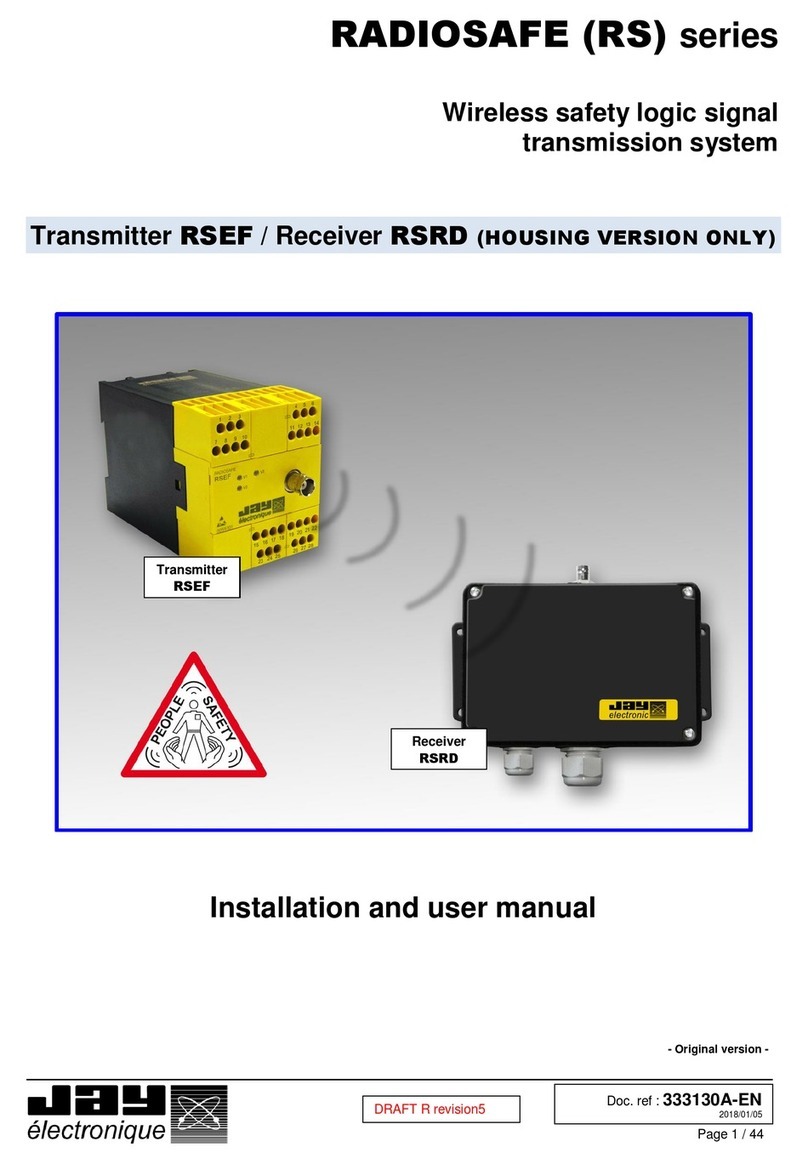
Jay electronique
Jay electronique RADIOSAFE Series Installation and user manual
Williams Sound
Williams Sound WIR 125 Manual and user guide
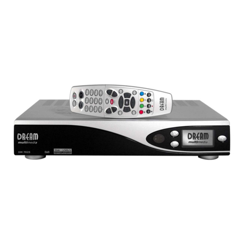
DREAM MULTIMEDIA
DREAM MULTIMEDIA Dreambox DM 7025 user manual
