Emcee TTU500FA User manual

Broadcast Products
P.O. Box 68, White Haven, PA 18661 Phone: (570) 443-9575 FAX: (570) 443-9257
MDS
MMDS
ITFS
LPTV
North America
South America
Europe
Asia
Australia
Africa
Since 1960
6) USERS MANUAL
TTU500FA
SOLID STATE LDMOS
500W UHF TRANSMITTER

TTU500FA
SOLID STATE LDMOS
500W UHF TRANSMITTER
05/01

IMPORTANT
Transient Overvoltage Protection
Transient overvoltageof micro- andnano-secondsdurationspresentonAC lines
are a continuous threat to all solid-state circuitry. The resulting costs of
equipment repairs and system downtime make preventative protection the best
insurance against thesesuddensurges. Types ofprotection rangefrom isolation
transformers and uninterruptible power supplies to the more cost effective AC
power line protectors. As transientsare most often caused by lightning induction
and switching surges, AC power line protectors are the most practical solution.
An effective AC power line protector is one capable of dissipating impulse
energy at a low enough voltage to ensure the safety of the electronic compo-
nents it is protecting. The protection unit should be across the AC line at all
times even during periodsof total blackout. It should also reset immediately and
automatically to be 100% ready for repeated transients.

TABLE OF CONTENTS
I. THE TTU500FA TRANSMITTER
1.1 Introduction
1.2 Specifications
1.3 Installation
1.4 Operation
1.5 Warrant
y
and Parts Orderin
g
II. CIRCUIT DESCRIPTION
2.1 Modulator
2.2 EMEX1 2 Watt UHF Exciter
2.3 500 Watt UHF Power Amplifier
2.4 Output Section
2.5 Control/Meterin
g
Panel
III. MAINTENANCE
3.1 Periodic Maintenance Schedule
3.2 Recommended Test E
q
uipment
3.3 Troubleshootin
g
3.4 Ali
g
nment
3.5 Output Power Calibration
3.6 Linearit
y
Corrector Ad
j
ustment
3.7 Remote Monitor Si
g
nal Levels
3.8 Spare Modules and Components
3.9 S
y
nthesizer Pro
g
rammin
g
IV. DATA PAK
V. SCHEMATIC DIAGRAMS

i
SECTION I
THE TTU500FA TRANSMITTER
1.1 INTRODUCTION ....................................................... 1
6
1
1.2 SPECIFICATIONS ..................................................... 1
6
1
1.3 INSTALLATION ........................................................ 1
6
3
1.4 OPERATION ........................................................... 1
6
4
1.5 WARRANTY AND PARTS ORDERING ................................... 1
6
5

1
6
1
SECTION I
THE TTU500FA TRANSMITTER
1.1 INTRODUCTION:
The EMCEE TTU500FA LPTV Transmitter is a remarkably compact design rated to provide
500 watts peak visual and 25 watts average aural power on any FCC specified channel extending
from 470 to 806MHz. The TTU500FA is completely solid-state supplying maximum performance
and reliability through the liberal utilization of Laterally Diffused Metal Oxide Semiconductors
(LDMOS). Comprised of a modulator, an EMEX1 2 Watt UHF Exciter, one 500 Watt UHF Amplifier
drawer, an Output Section for filtering and power measurement, and panels for power distribution
and metering/control, the TTU500FA is easy to service and maintain with RF alignment practically
nonexistent. A number of controls and indicators, furnished on the transmitter’s Control/Metering
panel and the EMEX1 Exciter front panel, provide convenient operation while displaying the results
of the transmitter's diagnostic circuitry.
The TTU500FA is designed for the express purpose of broadcasting as authorized by the U.S.
Federal Communications CommissionunderPart 74, Subpart G, of the FCC Rulesand Regulations.
1.2 SPECIFICATIONS:
Visual:
Output Power 500 watts peak
Emission 5M75C3F visual
Color Transmission NTSC, PAL, or SECAM
Output Frequency 470-806MHz
(FCC - Ch.14-69)
(CCIR - Ch.21-62)
Frequency Stability Visual Carrier ±500Hz
Output Power Stability ±0.5dB
Spurious Products
60dB below peak sync
Harmonics
60dB below peak sync
In-band Intermodulation (IM3)
52dB below peak sync
Differential Gain ±5%
Differential Phase ±3
(

1
6
2
Low Frequency Linearity 5%
Frequency Response ±0.5dB
Sideband Response Better than FCC 73.687(a)(1)
Envelope Delay Better than FCC 73.687(a)(3)
Output Impedance/Connector 50 ohms / 7/8" EIA flange
Video Signal to Noise
55dB
Video Input Level 1 volt peak-to-peak nominal
Video Input Impedance 75 ohms unbalanced
Aural:
Output Power 25 watts average
Emissions 250KF3E
Frequency Stability ±200Hz re. visual
Audio Input Level 0dBm nominal
Audio Input Impedance 600 ohms balanced
Audio Distortion <1%
FM Noise <
55dB
General/Mechanical:
Ambient Temperature
30
(
C to +50
(
C
Power Requirements 230Vac ± 15%, 1 phase, 50/60Hz, 4kW
Power Consumption: 2kW w/black picture
Power Factor 0.9
Mechanical Dimensions 48"H x 22"W x 31"D
Weight 300 lb.

1
6
3
1.3 INSTALLATION:
Except where otherwise noted, the connectors mentioned in the following instructions are located
on the rear of the transmitter.
1. After unpacking the transmitter, a thorough inspection should be conducted to reveal any
damage which may have occurred during shipment. If damage is found, immediately notify
the shipping agency and advise EMCEE Broadcast Products Customer Service or its field
representative. Also check to see that any connectors, cablesor miscellaneous equipment,
which may have been ordered separately, are included.
2. Place the transmitter in a clean, weatherproof environment providing adequate ventilation
for the exhaust fans at the rear of the transmitter drawers. It is important to maintain the
transmitter's ambient temperature within the
30
(
C and +50
(
C limits. Cooler ambient
temperatures will provide increased reliability.
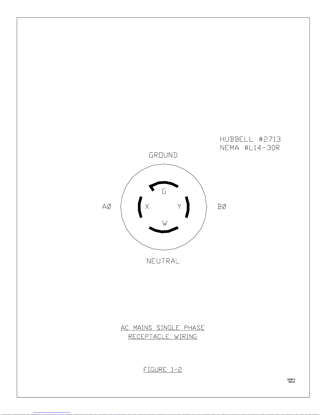
3. Place the transmitter in its permanent location near a single-phase receptacle that supplies
230Vac at 50/60Hz. The ac source should have a minimum power capacity of 4kW.
IMPORTANT
Do not apply ac power to the transmitter at this time since its RF output must be
properly loaded before being placed in operation.
4. Set all circuit breakers, including the customer's incoming ac line breaker, to the OFF
position. Ac breakers can be found on the transmitter’s AC Distribution Panel, at the rear of
the amplifier and Exciter drawers, and on the front AC Power panel. Place an appropriate
power line protector (surge suppressor) across the ac line that supplies the transmitter.
5. Connectthebasebandvideoandaudiocables(customersupplied)tothetransmitter's VIDEO
and AUDIO connectors located on the upper panel at the rear of the transmitter cabinet.
6. Connect the transmitting antenna cable (or a 1kW, 50 ohm dummy load) to the 7/8" EIA
flange connector marked RF OUTPUT located through the center rear of the cabinet’s top
cover.
7. Verify that the power cords of the Modulator (110V/15A), Exciter (110/15A) and 500W Power
Amplifier drawer (220V/20A)are plugged into the receptacles at the bottom of the transmitter
cabinet. Also check to see that any ancillary equipment included in the cabinet (i.e. Video
Detect Switch, Stereo Generator, etc.) are connected to the appropriate ac sockets.
8. Check to see that all RF cables and wire harnesses are properly connected and secure.
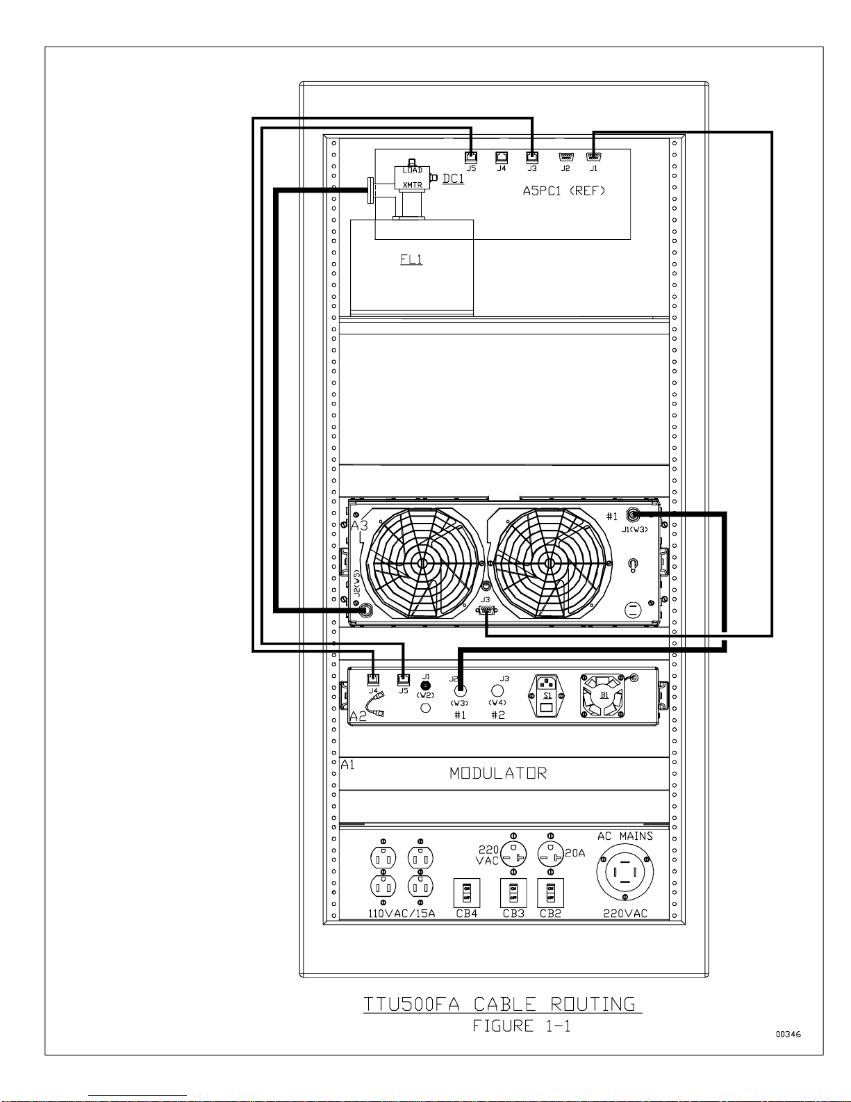
9. Usingthe4-prong, twist-lock, femaleplugsuppliedwiththetransmitter,fabricateanac power
cord (Figure 1
6
1) and plug it into the transmitter's AC MAINS connector at the bottom rear
of the transmitter cabinet. Open the incoming ac mains wall breaker and connect the other
end of the power cord into an appropriate 220Vac electrical outlet.

1
6
4
1.4 OPERATION:
Assuming the installation instructions of Section 1.3 have been completed and the transmitter is
receivingbasebandvideo and audiosignals, proceed with the following steps to place the transmitter
in operation. Except where otherwise noted, the controls, switches, and indicators mentioned in
these steps are located on the front of the transmitter.
1. Open the AC POWER circuit breaker located on the bottom front panel of the transmitter and
close the incoming ac mains breaker. Insure that the EMEX1 Exciter OPERATE/STANDBY
switch is in the off/out (STNDBY) position and the AGC/MANUAL button is in the off/out
(MANUAL) position. Place the transmitter’sControl/Metering panel FWD/REFL meter switch
to the FWD/out position.
2. Place the three AC Distribution Panel breakers (CB2, CB3, CB4), located at the lower rear
of the cabinet, to the on position. Also switch the Exciter and amplifier drawer rear panel
breakers to on.
3. Move the AC POWER circuit breaker located on the bottom front panel of the transmitter to
the ON position.
4. If applicable, place the Modulator's power switch to ON and verify that it is providing 87.5%
video modulation. If necessary, adjust the Modulator for the proper video depth of
modulation asdescribed in its instruction manual. Also check to see that the audio peaks are
not overmodulating the aural carrier.
5. Verify the following transmitter responses:
a. The fans at the rear of each drawer should be operating.
b. The Exciter’s green LED indicators should react as follows:
SYNTHESIZER LOCK – on
IF STATUS – on
AMPLIFIER STATUS – on
LINEARITY CORRECTOR – on
AGC ACTIVE – off
SWEEP MODE – off
OPERATE/STANDBY – off
VSWR RESET – off
AGC voltmeter – 1 segment lit at approximate center
RF POWER meter – 0%
c. The green LED indicators on the transmitter’s Control/Metering panel should respond
as follows:
AMPLIFIER TEMP – off
AMPLIFIER – on
POWER SUPPLY – off
RF POWER meter – 0%
FWD – on
REFL – off

1
6
5
6. Turn the Exciter's OUTPUT LEVEL ADJUST two or three turns counterclockwise and press
the OPERATE/STANDBY switch in to place the transmitter in OPERATE. Then verify the
following responses of the transmitter:
a. The Exciter’s OPERATE/STANDBY switch indicator is now lit green.
b. The POWER SUPPLY Control/Metering panel indicator is now lit green.
c. The status of all other indicators previously mentioned is the same.
7. Check to see that the Control/Metering panel’s meter switch is in the FWD/out position and
then slowly turn the Exciter’s OUTPUT LEVEL ADJUST clockwise until a 100% indication
appears on the Control/Metering panel’s RF POWER meter. The Exciter’s RF POWER
meter should also be displaying a 100% indication.
8. After 10 minutes of operation press the Exciter’s AGC/MANUAL switch in to engage the
transmitter’s output automatic gain control. If necessary and with a small tuning tool, slowly
turn the AGC LEVEL ADJUST to bring the transmitter’s RF POWER meter reading back to
100%.
9. Place the Control/Metering panel's meter switch to REFLD and verify that the RF POWER
meter indicates no more than 10% returned power. If the reflected power is more than 10%,
shutdownthe transmitter andcheck theVSWR of thetransmittingantenna anditsassociated
cable.
10. Place the Control/Metering panel's meter switch to FWD for constant monitoring of the
transmitter's final output power.
The transmitter is now in operation. Check its coverage area for clean, sharp television reception.
If the reception or picture quality is unsatisfactory, examine the amount of power delivered to the
transmitting antenna (see Section 3.5) and, if necessary, examine the antenna orientation and
antenna transmission line VSWR to insure maximum radiation in the proper direction.
1.5 WARRANTY AND PARTS ORDERING:
Warranty – EMCEE warrants its equipment to be free from defectsin material and workmanship for
a period of one year after delivery to the customer. Equipment orcomponents returned as defective
(prepaid) will be, at our option, repaired or replaced at no charge as long as the equipment or
component part in question has not been improperly used or damaged by external causes
(e.g., water, ac line transients or lightning). Semiconductors are excepted from this warranty and
shall be warranted for a period of not more than ninety (90)daysfrom date of shipment. Equipment
or component parts sold or used by EMCEE, but manufactured by others, shall carry the same
warranty as extended to EMCEE by the original manufacturer.
Equipment Returns – If the customer desires to return a unit, drawer, or module to EMCEE for
repair, follow the procedure described below:
1. Contact EMCEE Customer Service Department by phone or fax for a Return Authorization
Number.

1
6
6
2. Provide Customer Service with the following information:
Equipment model and serial numbers.
Date of purchase.
Unit input and output frequencies.
Part number (PN) and Schematic Diagram designator if a module is being sent.
Detailed information concerning the nature of the malfunction.
The customer shall designate the mode of shipping desired (e.g., Air Freight, UPS, Fed Ex, etc.).
EMCEE will not be responsible for damage to the material while in transit. Therefore, it is of utmost
importance that the customer insure the returned item is properly packed.
Parts Ordering – If the customer desires to purchase parts or modules, utilize the following
procedure:
1. Contact EMCEE Customer Service by phone or fax indicating the customer's purchase order
number. If thepurchaseorder number isprovidedbyphone, writtenconfirmation of theorder
is required.
2. Also provide:
The equipment model and serial number.
The unit input and output frequencies.
The quantity, description, vendor, number, and designation of the parts needed as found in
the Parts Lists subsection of this manual.
If a module is required, give the part number (PN) and Schematic Diagram designator
(e.g., 30404029).
Designate the mode of shipping desired (e.g., Air Freight, UPS, Fed Ex, etc.).
Shipping and billing addresses.
Spare and Replacement Parts – The Spare Modules and Components section of this manual
provides a detailed listing of the modules and some discrete components contained within the
transmitter. The listing contains those modules or components considered to be essential
bench-stock items and should be available to the technician at all times. The Schematic or
Interconnection Diagram isthegoverning document of this manual. Should there be a discrepancy
between a modules or components list and a diagram, the diagram takes precedence. Such a
discrepancy is possible since manufacturing changes cannot always be incorporated immediately
into the instruction manual.
Component Referencing – A transmitter may consist of a modulator or receiver, a number of
modules and components mounted in drawers, and components or modules mounted to panels or
directly to the cabinet. Components mounted in a module which is included in a drawer take the
drawer number and the module number in addition to a component number. Thus the reference
designator A2A1Q1 means transistor Q1 in module A1 of drawer A2. Components mounted in a
drawer takeonly the drawer number and a component number (e.g., A2M1 designates meter M1 of
drawer A2). Components mounted directly to a panel take only the panel number and a component
number. Components and modules mounted directly to the cabinet take only a component or
module number.

1
6
7
For EMERGENCY technical assistance, EMCEE offers atoll free,24-hour, 7-day-a-week
customer service hot line: 1-800-233-6193.


ii
SECTION II
CIRCUIT DESCRIPTION
2.1 MODULATOR ......................................................... 2
6
1
2.1a Video Detector Switch ............................................... 2
6
1
2.2 EMEX1 2 WATT UHF EXCITER ......................................... 2
6
1
2.2a Linearity Corrector .................................................. 2
6
2
2.2b IF/Converter ....................................................... 2
6
3
2.2c UHFSynthesizer ................................................... 2
6
6
2.2d Reference Oscillator ................................................. 2
6
7
2.2e UHF Bandpass Filter ................................................ 2
6
7
2.2f 2WattUHFAmplifier................................................ 2
6
7
2.2g Metering Coupler ................................................... 2
6
9
2.2h MeteringDetector................................................... 2
6
9
2.2i Control/Interface Board .............................................. 2
6
9
2.2j Display/MonitorBoard .............................................. 2
6
20
2.2k 28V/15V/5V Power Supply ........................................... 2
6
24
2.3 500 WATT UHF POWER AMPLIFIER DRAWER ......................... 2
6
24
2.3a PowerSplitter..................................................... 2
6
25
2.3b 300W UHF Power Amplifier .......................................... 2
6
25
2.3c PowerCombiner................................................... 2
6
27
2.3d AmplifierStatusInterface............................................ 2
6
27
2.3e Power Supply/Thermal Interface ....................................... 2
6
27
2.3f 32V Power Supply ................................................. 2
6
28
2.4 OUTPUT SECTION ................................................... 2
6
29
2.4a UHF Bandpass Filter ............................................... 2
6
29
2.4b Directional Coupler ................................................. 2
6
29
2.4c MeteringDetector.................................................. 2
6
29
2.5 CONTROL/METERING PANEL ......................................... 2
6
30
2.5a Control/Monitor Board .............................................. 2
6
30

2
6
1
SECTION II
CIRCUIT DESCRIPTION
2.1 MODULATOR:
EMCEE EM1 / Scientific Atlanta 6340 / RF Comm. 2000
t
A1
IF OUT
8dBm peak visual typical
The modulator processes baseband video and audio signals to provide a composite IF output
composed of a visual carrier at 45.75MHz with 5M75C3F modulation, and an aural carrier at
41.25MHz with 250KF3E modulation. Any of these modulators can be used to drive the EMEX1
2 Watt Exciter drawer (A2). The optional video sense circuit provides an indication of whether the
modulator is receiving a baseband video signal. The output of the video sense is either a logic
high (
+5Vdc) with video present or a logic low (
0Vdc) when video is not present. This logic
signal is used by the Exciter Control/Interface Board (A2PC1) to place the transmitter in standby
if the video signal is lost.
2.1a Video Detector Switch:
Burst VDS
t
A9
For those modulators which do not contain a video sense alarm, the Burst Electronics Video
Detector Switch (Model VDS) will be installed in the transmitter cabinet. The VDS detects the
presenceofcompositevideo connected toitsA INPUT directly from the VIDEO connector mounted
on the Video/Audio/Remote Panel (A8J2). If a loss of video is detected, then the unit switches to
the B INPUT, lights its red LED and energizes an internal TALLY relay. Through this relay, a
ground is sent to the Exciter Control/Interface circuit via the transmitter’s Control/Monitor board
(A5PC1) placing the transmitter in a nonradiating condition.
2.2 EMEX1 2 WATT UHF EXCITER:
Interconnection Diagram 40404001/Rev 55
t
A2
Composite IF IN (J1)
8dBm peak visual
21dBm average aural
RF OUT (J2 & J3)
+18dBm typical peak visual
+5dBm typical average aural
The EMEX1 Exciter drawer converts the composite IF signal from the modulator to the desired
UHFfrequency while amplifyingthisRF signal to the appropriateoutputlevel. TheExcitersupplies
approximately 200mW of peak visual power to drive the 500W UHF Power Amplifier drawer (A3).
Power control, automatic gain control (AGC) and heterodyne conversion are performed by the
IF/Converter module (PC1). Utilizing the composite IF signal, the Linearity Corrector furnishes
performance improvements for the transmitter’s ICPM, differential phaseand gain, syncamplitude

2
6
2
andintermodulation. The UHFSynthesizersuppliesaprogrammableLOtotheIF/Converter mixer
where the LO and IF signalsare combined to create the desired UHF frequency. The UHF signal
from the Converter module is then passed through the UHF Bandpass Filter (FL1) to remove the
unwanted LO and sum products from the conversion process while passing and amplifying the
desired difference signals. The signal is then amplified approximately 25dB by the 2 Watt UHF
amplifier (A1) and passed through the Metering Coupler (CP1). Here, a forward RF sample is
provided for useby the Metering Detector (A3) while the main signal is passed to the output of the
drawer.
Metering and control functions are provided by the Metering Detector, the Display/Monitor board
(PC3) and the Control/Interface Board (PC4). The Display/Monitor Board has several status and
diagnostic LED indicators which are presented on the Exciter’s front panel. The Control/Interface
board provides for various controls and logic circuits for proper operation of the transmitter. Dc
powerforthe Exciterissupplied by asmall, efficient multioutput switchingpowersupplyPS1which
furnishes ±28, ±15 and ±5 volts.
2.2a Linearity Corrector:
Schematic Diagram 40404011/Rev 55
t
A2PC2
IF IN (J1)
11dBm typical
IF OUT (J2)
12dBm typical
Gain with S1 ENABLE/DISABLE (J1-J2) 0 to
2dB typical
Current Draw 610mA @ +15Vdc
TheLinearityCorrectorisasix-stage, unitygaincircuitwhichcompensatesfor nonlinear distortions
generated inthetransmitter'sClassAB500 Watt Power Amplifier drawer. Whenproperly adjusted,
it provides correction to the transmitter’s output signal for sync amplitude, differential gain,
differential phase, ICPM and intermodulation. Corrector amplifiers U1 through U8 are all
monolithic amplifier stages providing approximately 12dB of gain per device. A phase correction
network is centered around amplifiers U2 through U5 while the circuitry surrounding U7 and U8
corrects for differential gain and sync compression. When properly adjusted, the phase and gain
correction networks will collectively reduce intermodulation distortion.
Input amplifier U1 is biased through resistor R1 and inductor L1 which acts as an RF choke.
Capacitor C2 is utilized as a B+ bypass with coupling capacitors C1 and C3 advancing the input
signal to the matching T-attenuator made up of resistors R2, R3 and R4. At hybrid splitter DC1,
the IF carrier is divided into two equal amplitude signals which are 90
(
out of phase. At the
splitter’s
90
(
port, a negative phase-shift network composed of inductor L3 and capacitors C15
through C18 adds another
22.5
(
shift to the signal (
112.5
(
total) before amplification by U3.
Conversely, connected to the 0
(
port of the splitter is a positive phase-shift network comprised of
inductor L2 and capacitors C4 throughC7. Here the 0
(
signal is shifted in the positive direction by
22.5
(
resulting in a 135
(
total difference between the two signals. In order to keep the amplitude
of each signal similar, the circuits surrounding amplifiers U2 through U5 are essentially identical
with the same biasing, bypassing and coupling described for U1. Transformers T3 and T4 on the
negative shift side of the circuit are 2:1 step-up types identical to T1 and T2, but necessary to
efficientlydrivegain expansiondiodesCR1andCR2. Throughadjustment of slopepotentiometers
R15 and R25 and threshold (cut-in) pots R21 and R30, the amplitude of the negative shifted signal
can be varied to add to or subtract from the positive shifted signal at in-phase combiner CP1.
When adjusted properly, this circuit can then correct the differential phase, intermodulation and
ICPM distortions created by the transmitter’s power amplifier. At the output of combiner CP1 the

2
6
3
IF signal passes through a matching pi-attenuator comprised of resistors R35, R36 and R37 before
amplification by U6, U7 and U8. Transformers T5 and T6 again double the signal voltage to
properly drive the gain expansion diodes CR3 and CR4 which compensate for differential gain and
sync compression created in the 500 Watt Power Amplifier (A3).
Thevariablegainexpansionnetworks,whichprovidelinearitycorrection,arecenteredarounddual
diodes CR1 through CR4, slope potentiometers R15, R25, R41, R57, unity gain dc amplifiers U9,
U10, U11, threshold potentiometers R21, R30, R47, R55 and ENABLE/BYPASS switch S1. The
threshold (cut-in) potentiometers determine the point on the IF waveform where the correction, or
gain expansion, willoccurandtheslope potentiometersdictate theamount of correction/expansion
to be used at that breakpoint. With S1 in the ENABLE position, the four diode pairs form nonlinear
circuits where each diode is reverse biased and the amount of reverse bias dictates the point at
which the diode turns on during the positive and negative cycles of the visual IF carrier envelope.
Eachdiodeisbiasedusingvoltagesestablishedby thethresholdpotentiometersin conjunction with
dc amplifiers U9, U10, U11 and U12. L4 through L6 and L9 through L12 isolate the IF signal from
the diode threshold biasing circuitry. When the positive and negative peaks of the visual signal
envelope are sufficient to forward bias a diode pair, the pair turns on placing the resistance of its
respective slope potentiometer in parallel with the series arm of its L-pad (R14, R24, R40, R50).
As a result, the attenuation of the visual IF carrier is reduced during this period causing the
waveform to stretch. Slope control R41 is typically used to correct differential gain while R57
primarily adjusts sync amplitude.
With S1 in the BYPASS position, ground is applied to FET switches Q1 and Q2 placing each diode
pair in hard reverse bias preventing conduction throughoutthe positive and negative cycles of the
IF carrier envelope. Due to the high reverse resistance provided, each diode network essentially
represents a resistive L-pad (R14/R16, R24/R31, R40/R42, R50/R58) with the IF signal attenuated
by a fixed amount in each location. As a result, no linearity correction is provided.
2.2b IF/Converter:
Schematic Diagram 40404021/Rev 53
t
A2PC1
IF INPUT (J1) 0dBm to
30dBm peak visual
CORRECTOR LOOP Out (J3)
11dBm peak visual typical
CORRECTOR LOOP In (J4)
12dBm peak visual typical
RF OUT
10 to
18dBm
LO INPUT (J5) +13dBm minimum
Current Draw 42mA @ +15V
31mA @
15V
185mA @ +5V
The IF/Converter performs three tasks in this transmitter. With thefirst AGC loop it furnisheslevel
control for the incoming signal from the modulator, upconverts the IF signal to the desired UHF
channel and then controls the transmitter’s output power through a second gain control loop.
The modulator’s IF input, provided at J1, is amplified or attenuated by variable gain amplifier U1.
This integrated circuit, controlled by the output of integrator U4 via switch S1, (U1) can produce
wide variations in gain ranging from +30dB to
10dB. At the output of U1 is coupling capacitor C3
and 2:1 step-down transformer T1 required for proper impedance matching between U1 and in-
phase splitter CP1. At the output of CP1, twoequal amplitude IF signals are delivered for differing
applications. The signal at pin CP1-3 is used to provide a reference for the input AGC loop, while

2
6
4
the second signal at pin CP1-4 is fed to the Linearity Corrector (PC2) connected to output J3. Both
signals pass through attenuators (3dB and 7dB respectively) which are connected to identical
monolithic amplifiers, U7 and U8. Thesedevices, offering approximately 14dB of signal gain, are
furnished bias through resistors R15/R22 and RF chokes L1/L2. The output of amplifier U8 is
connected, through coupling capacitor C19, to a variable PIN attenuator composed of diodes CR7
and CR8. This diode array forms a pi-attenuator operated by buffer U9 whose input (pin 5) is
supplied control voltage from the Exciter’s front panel OUTPUT LEVEL ADJUST. With maximum
voltage from U9 (+15V) the attenuator will exhibit minimum attenuation of approximately 2dB.
With minimum voltage the attenuator can provide more than 50dB of loss to the signal. This
attenuator is utilized as the main power control and standby mechanism for the transmitter.
At the output pin 3 of U7 is the second IF signal required by the input AGC circuit as a power
referencerepresenting the incoming modulator signal level. Thissignal is passedthrough coupling
capacitor C16 to integrated circuit U6, an RMS detector. At pin 7,U6 outputs the video component
of the IF visual carrier while C11 rolls off the aural energy contained in the signal. The amplitude
of the video is then doubled using op-amp U5A and then sent to peak detector CR3 via pins 1 and
2 of jumper JP1. (Pins 2 and 3 of JP1 are utilized for average digital power detection only.)
Capacitor C9 and resistor R10 filter the peak video component from diode CR3 and this dc voltage
is sent to unity gain buffer U5B. The dc level at the output of U5B (pin 7), which is now
proportional to the peak power of the visual signal entering the IF/Converter, will be approximately
+3V when the modulator level into the Converter board is at the midpoint of its input AGC window
(
15dBm peak). This potential then appears at pin 6 of integratorU4B where it is compared to the
voltage on pin 5 (
+3V) generated by divider R7/R8. When the values of each voltage at pins 5
and 6 are equal, the output of U4B at pin 7 will be zero, holding variable gain amplifier U1 at the
center of its gain extremes (+10dB) via pins 8 and 1 of electronic switch S1. (The gain of U1 can
also be set to its center by applying a low to the INPUT AGC CONTROL line which is connected
to pin 6 (IN) of switch S1. This low, supplied by the OPERATE/SWEEP switch PC4S1 on the
Control/Interface board, will disconnect the input AGC voltage at S1-8 from S1-1 and connect the
ground at S1-2, 3 to S1-1 effectively placing a zero voltage on pin 1 of U1.) If the input level from
the modulator at J1 increases, the outputs of U7, U6, U5Aand U5B will also increase forcing pin 7
of U4B negative and proportionally reducing the gain of U1. Conversely, if the input from the
modulator were to be reduced, the output of U4B would swing positive causing U1 to increase its
gain compensating for the signal reduction. Under normal transmitter operating conditions, the
signal provided at theCORRECTORLOOP output (J3) willbeapproximately
11dBm peak visual.
However, if the IF signal is significantly reduced (
25dBm) or removed completely, the potential
at the output of U4B will exceed +2.5V causing the level at input pin 2 of U4A to exceed the
reference (2.5V) provided at pin 3 through divider R5/R6. This action would drive output pin 1 of
U4A to zero, turning off the IF STATUS light (PC3DS5) on the Exciter’s front panel and placing a
low on the LEVEL ADJUST lineattached to pin 5 of U9 increasing the attenuation of the associated
PIN diode circuit to maximum (
50dB).
After proceeding through the Linearity Corrector, the IF signal is fed to CORRECTOR LOOP input
J4 at an approximate level of
12dBm. Here the signal is furnished a 50 ohm match using
pi-attenuator R30/R31/R32. Hybrid amplifier U1, biased through resistor R33 and RF choke L3,
provides 14dB of gain and delivers the signal to in-phase2-way splitter CP2 via coupling capacitor
C29. At output pins 3 and 4 of CP2 are two equal amplitude IF signals used, respectively, to drive
the output AGC loop (U13 through U18) and to bemixed to the wanted UHF channel after passing
through the output control attenuator. Made up of PIN diodes CR9/CR10 and controlled by U18,
this attenuator is capable of 2dB to 50dB of attenuation and ultimately sets the output power of the
transmitter. From the output control attenuator the IF signal is transferred to mixer MX1 through
coupling capacitor C51 and pins 1 and 2 of jumper JP3. (Connecting pins 2 and 3 of JP3 brings
the IF signal to test point TP1.) In MX1 the IF is then upconverted to the desired UHF signal as
a result of combining with the local oscillator frequency presented at LO INPUT J5. At the output
of the mixer (pin 4) resistors R67/R68/R69 provide 5dB of attenuation and the appropriate
Table of contents
Other Emcee Transmitter manuals


