LBI4898
TABLE
OF
CONTENfS
SPECIFICATIONS
................................................................
.
Cover
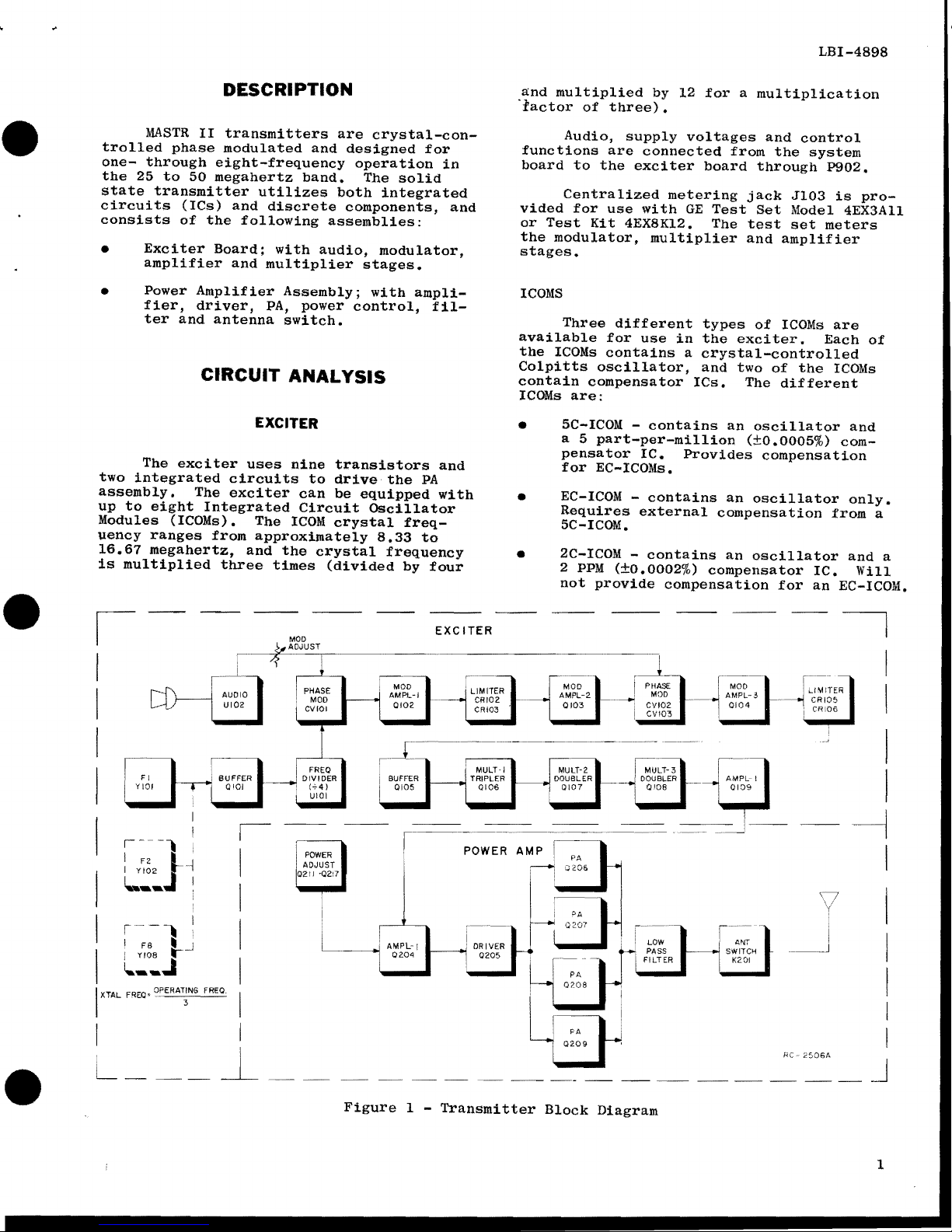
DESCRIPTION
.................................................................•..
1
CIRCUIT ANALYSIS
..............................................................
. 1
Exciter
..................................................................
. 1
ICOMs
...............................................................
. 1
Audio
IC
............................................................
. 3
Frequency
Divider
...................................................
. 4
Phase
Modulators,
Amplifiers
and
Multipliers
........................
. 4
Power
Amplifier
..................................•........................
5
RF
Amplifiers
.......................................................
. 5
Power
Control
Circuit
...............................................
. 6
Carrier
Control
Timer
....................................................
. 6
MAINTENANCE
...................................................................
. 6
Disassembly
...............................................•...............
6
PA
Transistor
Replacement
................................................
. 7
Alignment
Procedure
......................................................
. 9
Test
Procedures
..........................................................
.
10
Power
Output
........................................................
.
10
Tone
Deviation
......................................................
.
10
Voice
Deviation
.....................................................
.
10
Troubleshooting
..........................................................
.
11
OUTLINE
DIAGRAM
...............................................................
.
12
SCHEMATIC
DIAGRAMS
(with
voltage
readings)
Exciter
..................................................................
. 14
Power
Amplifier
..........................................................
.
15
PARTS
LIST
AND
PRODUCTION
CHANGES
Exciter
..................................................................
. 13
Power
Amplifier
..........................................................
.
16
-
18
ILLUSTRATIONS
Figure
l -
Block
Diagram
......................................................
.
Figure
2-
Typical
Crystal
Characteristics
....................................
.
Figure
3 -
Equivalent
!COM
Circuit
............................................
.
Figure
4 -
Simplified
Audio
IC
................................................
.
Figure
5 -
Disassembly
Procedure
(Top
View)
...................................
.
Figure
6-
Disassembly
Procedure
(Bottom
View)
................................
.
Figure
7 -
PA
Transistor
Lead
Identification
......................•............
Figure
8 -
PA
Transistor
Lead
Forming
.........................................
.
Figure
9-
Frequency
Characteristics
Vs.
Temperature
..........................
.
Figure
10-
Power
Output
Setting
Chart
.........................................
.
1
2
3
4
7
7
8
8
9
9
WARNING
----------------------------------------,
ii
Although
the
highest
DC
voltage
in
MASTR
II
Mobile
Equipment
is
supplied
by
the
vehicle
battery,
high
currents
may
be
drawn
under
short
circuit
conditions.
These
currents
can
possibly
heat
metal
objects
such
as
tools,
rings,
watchbands,
etc.,
enough
to
cause
burns.
Be
careful
when
working
near
energized
circuits!
High-level
RF
energy
in
the
transmitter
Power
Amplifier
assembly
can
cause
RF
burns
upon
contact.
KEEP
AWAY
FROM
THESE CIRCUITS
WHEN
THE
TRANSMITTER
IS
ENERGIZED!
,.
•
•
•