ENDAT 4066i User manual

User’s Manual I
ENDAT-4066i
User’s Manual
Rev. 1A
4066i PCB ver: A2 or later
25/05/2007
II
The ENDAT-4066i System Board
Copyright Notice
The content of this manual has been checked for accuracy. The manufacturer
assumes no responsibility for any inaccuracies that may be contained in this
manual. The manufacturer reserves the right to make improvements or
modification to this document and/or the product at any time without prior
notice. No part of this document may be reproduced, transmitted, photocopied or
translated into any language, in any form or by any means, electronic, mechanical,
magnetic, optical or chemical, without the prior written permission of the
manufacturer.
Intel® Pentium4®, Celeron® and Celeron D ® is registered trademark of Intel
Incorporation
Multiscan is a trademark of Sony Corp of America
IBM, EGA, VGA, PC/XT, PC/AT, OS/2 and PS/2 are registered trademarks of
International Business Machines Corporation
Plug and Play is registered trademarks of Intel Corporation
Microsoft, Windows and MS-DOS are trademarks of Microsoft Corporation
Award is a trademark of Phoenix Software Inc.
PCI is a registered trademark of PCI Special Interest Group
Other product names mentioned herein are used for identification purpose only and
may be trademarks and/or registered trademarks of their respective companies.
Installation Notice
The manufacturer recommends using a grounded plug to ensure proper
motherboard operation. Care should be used in proper conjunction with a
grounded power receptacle to avoid possible electrical shock. All integrated circuits
on this motherboard are sensitive to static electricity. To avoid damaging
components from electrostatic discharge, please do not remove the board from the
anti-static packing before discharging any static electricity to your body, by wearing
a wrist-grounding strap. The manufacturer is not responsible for any damage to the
motherboard due to improper operation.

User’s Manual III
Specification:
Model ENDAT-4066i
Form Factor Mini-ITX 170 mm x 170 mm (6.69”x6.69”)
System Chipset INTEL 865GV + ICH5
CPU Supporting 533/400 FSB with 478 pin PENTIUM4/Celeron/Celeron D processor
Memory 1 x 184 pin DDR socket support DDR 400/333/266 up to 1GB
Ethernet INTEL 82801ER/EB (ICH5) + PHY (Intel 82562EX)
VGA INTEL 865GV Graphic Controller with DVMT up to 96MB(max)
LCD interface Onboard LVDS support 18/24/36/48bit Single/Dual Channels via internal
box header (optional)
Display ratio 4:3 and 16:9
Serial / Parallel 2 Serial Port w/+5V, +12V Power Selector / 1 Parallel port (Optional to 6
Serial ports via I/O kit)
Watchdog Timer Winbond 83627THG on-chip support 1 to 255 seconds/minutes
IDE Connector 1 x 40pin IDE connector support UDMA 33/66/100
1 x 44pin IDE connector support Slim type HDD
SATA Connector Support 1 port 150MHz Serial ATA Device
AUDIO On-board support AC'97 with 1.2W amplifier
CMOS backup EEPROM backup customized setting in system BIOS
Expansion Slot One PCI expansion up to 3 PCI slots via riser card with PCI 2.2 compliance
PS/2 Keyboard / Mouse Connector
2 x USB (2.0) + RJ-45 Connector w/LED indicator
D-sub Connector for COM 1,2 (internal box header for COM2) with
POWER
1 x 25 Pins D-Sub Connector (LPT)
1 D-Sub Connector (VGA)
MIC-IN, Line-In, SPK-Out with COM2 Module Deck
I/O Port
Internal pin header: KB, MS, USB (2.0) x4, AUX/CD-IN, SPDIF IN/OUT, RF
MIC IN, IR
Digital IO 2 bit input and 2 bit output (TTL level) by pin header
RS-422/485 Via COM2 (Optional)
USB Port 6 x USB2.0 onboard
Power Supply Support P4-ATX power supply
IV The ENDAT-4066i System Board
TABLE OF CONTENTS
CHAPTER 1. INTRODUCTION .......................................................1
1-1. FEATURES..............................................................................................2
1-2. UNPACKING............................................................................................ 3
1-3. ELECTROSTATIC DISCHARGE PRECAUTIONS................................... 3
1-4. MOTHERBOARD LAYOUT...................................................................... 4
CHAPTER 2. SETTING UP THE MOTHERBOARD.......................5
2-1. JUMPERS AND CONNECTORS.............................................................. 5
2-2. INSTALLING MEMORY.......................................................................... 14
2-3. SHARED VGA MEMORY....................................................................... 14
2-4. INSTALLING RISER CARD.................................................................... 14
2-5. ASSIGNING IRQs FOR EXPANSION CARDS ....................................... 14
2-6. WATCHDOG TIMER…………………………………………………………. 15
2-7. DIGITAL I/O…………………………………………………………...………. 17
CHAPTER 3. AWARD BIOS SETUP.............................................18
3-1. STANDARD CMOS FEATURES............................................................. 19
3-2. ADVANCED BIOS FEATURES............................................................... 20
3-3. ADVANCED CHIPSET FEATURES........................................................ 21
3-4. INTEGRATED PERIPHERALS............................................................... 23
3-5. POWER MANAGEMENT SETUP........................................................... 27
3-6. PnP/PCI CONFIGURATIONS................................................................. 28
3-7. PC HEALTH STATUS............................................................................. 29
3-8. FREQUENCY/VOLTAGE CONTROL ..................................................... 29

User’s Manual V
CHPATER 4. VGA, LCD, FEATURE..............................................31
4-1. VGA FEATURE....................................................................................... 31
4-2. LVDS PANELAND TV FEATURE........................................................... 32
4-3. PCI BUS AUDIO ADAPTER FEATURES................................................ 33
4-4. DRIVER UTILITY INSTALLATION GUIDE ............................................. 34
CHPATER 5. LAN ADAPTER........................................................35
5-1. FEATURES ............................................................................................ 35
5-2. UTP CABLE/RJ-45 JACK DEFINITION.................................................. 36
5-3. CONNECTING 100BASE-TX FAST ETHERNET NETWORK ................ 37
5-4. CONNECTING 10BASE-T ETHERNET NETWORK ..............................37
5-5. 10MBASE/ 100MBASE INSTALLATION NOTICE .................................. 37
5-6. REMOTE BOOT ROM FUNCTION ........................................................ 38
5-7. LED INDICATORS.................................................................................. 38
APPENDIX A: FLASH MEMORY UTILITY....................................39
APPENDIX B: CONNECTOR PIN ASSIGNMENT........................40
APPENDIX C: UC-COM56 JUMPER SETTING............................41
APPENDIX D: LIMITED WARRANTY...........................................42

User’s Manual 1
Chapter 1. Introduction
ENDAT-4066i supports high performance processor of Intel® Pentium4®,
Celeron® and Celeron D ® with 400 and 533 Front Side Bus. It also supports high
speed DDR memory with 64-bit wide interfaces with non-ECC DIMM (up to 1GB).
Only Double Data Rate (DDR) SDRAM memory is supported and the speed of
memory can be 266, 333 and 400 MHz.
ENDAT-4066i provides an integrated graphics (Intel® Extreme Graphics 2)
accelerator delivering cost competitive 3D, 2D, and video capabilities.
ENDAT-4066i video engines support video conferencing and other video
applications. Instead of a dedicated local graphics memory interface, ENDAT-4066i
uses a UMA configuration for optimal memory utilization and performance that
deliver 3D graphics with sharp images, fast rendering, smooth motion and extreme
detail.
ENDAT-4066i contains one integrated Serial ATA host controllers capable of
independent DMA operation on two ports. The SATA controllers are completely
software transparent with the IDE interface, while providing a lower pin count and
higher performance. The data transfer rate is up to 150 MB/s.
ENDAT-4066i is an ideal model for various kind of application:
-POS system
-KIOSK
-Interactive system
-Airport Terminal Controller
-Industrial controller
-Digital entertainment
-Embedded system equipment
2The ENDAT-4066i System Board
1-1.Features
Basic Feature:
zBoard format: Mini-ITX (170mm x 170 mm)
zSupports Socket 478 CPU (FSB 533/400 MHz)
zDigital I/O: 2 bits in and 2 bits out (3.3V)
zSupports DDR 266/ 333/ 400 SDRAM up to 1GB
zSerial ATA connector x 1
zEnhance IDE connector x 2
zMultiple I/O ports: COM port x 2; USB (2.0) x 6
zAll COM ports with +5V, +12V power selector
zCMOS backup: EEPROM backup
zWatchdog Timer
zIntel 10/100 LAN andAudio function onboard
zWith Intel embeddedATX PCI expansion design
Optional features:
zOn board chip provides LVDS interface (18/24/36/48 bit, single/dual
channels) or TV out signals (composite and S-video)
zSecond I/O kit for extra 4 COM ports (COM3 to COM6)
zRS 422/485 via COM 2
zBarebones system: niche into Unicorn U-8000 Chassis
Full Software Support:
zDrivers for major operating systems and APIs: Windows 9x / ME,
Windows 2000, Windows XP, Direct3D, DirectDraw and DirectShow,
OpenGL ICD for Windows 9x, and 2000, and DXVA for Windows
2000 and Windows XP

User’s Manual 3
1-2. Unpacking
The motherboard comes securely packaged in a sturdy cardboard shipping carton.
In addition to the User's Manual, the motherboard package includes the following
items:
ENDAT-4066i System Board
HDD / IO Cables
LCD cable (Optional)
CDROM Driver includes: Drivers for Windows 98, ME, 2000, XP and AMI / AWARD
FLASH ROM utilities.
Driver utilities for on-board VGA drivers, LAN adapter
If any of these items are missing or damage, please contact the dealer from whom
you purchase the motherboard. Save the shipping material and carton in the event
that you want to ship or store the board in the future.
Note:
Please leave the motherboard in its original package until you are
ready to install it!
1-3. Electrostatic Discharge Precautions
Make sure you properly ground yourself before handling the motherboard, or other
system components. Electrostatic discharge can easily damage the components.
Note: You must take special precaution when handling the motherboard in dry or
air-conditioned environments.
4The ENDAT-4066i System Board
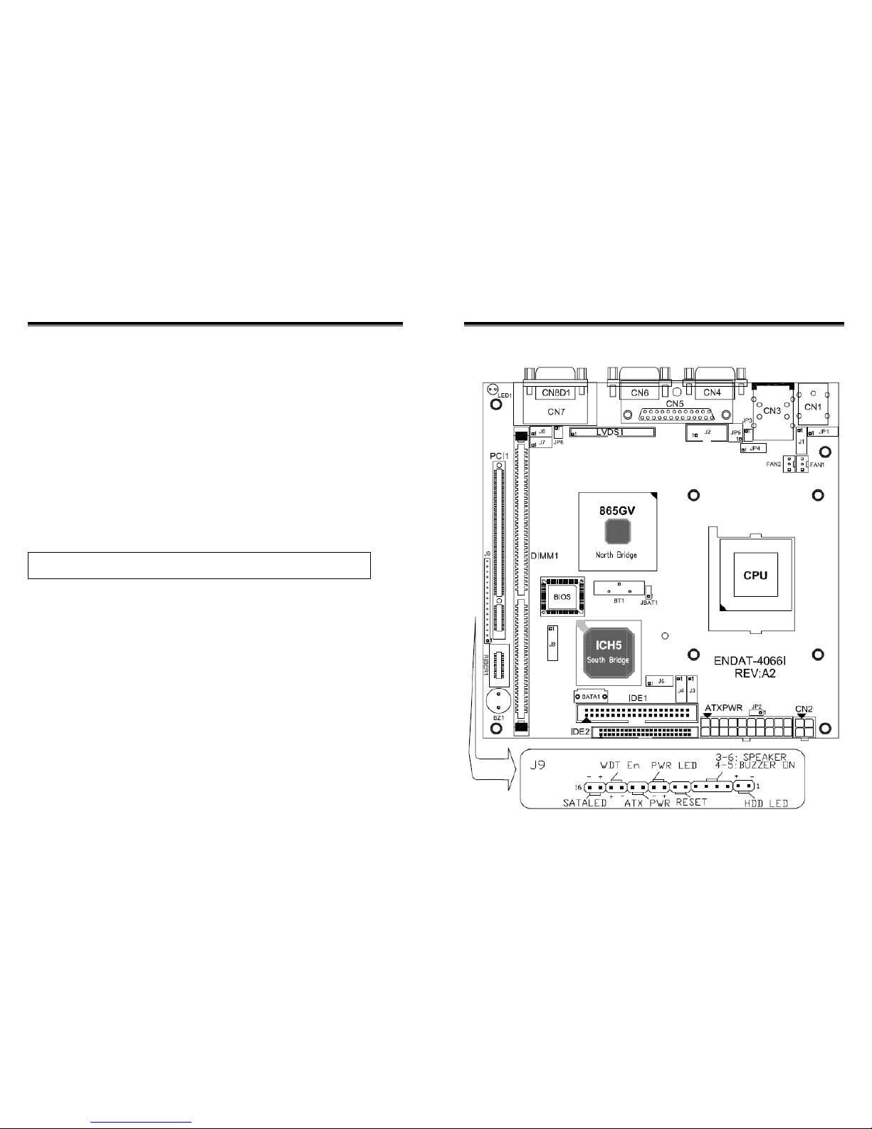
1-4. Motherboard Layout

User’s Manual 5
Chapter 2. Setting up the Motherboard
2-1. Jumpers And Connectors
Jumpers/Connectors Overview:
Function Jumpers/Connectors
Cooling Fan Connector FAN1, FAN2
P4 Power Supply Connector 2*2 CN2
P4 Power Supply Connector 2*10 ATXPWR
LCD Panel Connector LVDS1
LCD Voltage Selector JP6
Clear CMOS JBAT1
Pin Header for external device JP1
PS/2 Mouse/KB Pin Header J1
PS/2 Mouse/KB CN1
USB Port CN3, J3, J4
IDE 1, IDE 2 IDE1, IDE2
SATA 1 SATA1
IDE active LED J9: Pin 1(-), Pin 2(+)
External Speaker J9: Pin 3, Pin 6
Buzzer On/Off J9: Pin 4, Pin 5
Hardware Reset Switch J9: Pin 7, Pin 8
Power LED J9: Pin 9(+), Pin 10(-)
ATX Power Supply On/Off Switch J9: Pin 11, Pin 12
WDT Function Enable/Disable J9: Pin 13, Pin 14
SATA LED J9: Pin 15(+), Pin 16(-)
DDR SDRAM socket DIMM1
LAN Connector CN3
CRT Output CN6
Power Good Selector JP2
COM1 & COM2 Voltage Selector JP4
COM1 CN4
COM2 CN8D1
LPT1 CN5
MIC In, Line In, Line Out CN7
COM2 Pin Header J2
RS232 / 485 Selector for COM2 JP3 & JP5
6The ENDAT-4066i System Board
Function Jumpers/Connectors
DIGITAL I/O Pin Header J5
CD In & Line Out Pin Header J6
Microphone IN & LINE IN Pin Header J7
LPC Super I/O Connector J8
Please double-check the insertion and orientation of the LCD cable
before applying power. Improper installation will result in permanent
damage LCD panel.
Part 1: Onboard Jumpers
JP1: Pin Header for external device (2.0mm)
Pin No. Signal (MS) Pin No. Signal (KB)
1 MS Data Out 2 KB Data Out
3 MS Data In 4 KB Data In
5 MS Data Out 6 KB CK Out
7 MS CK In 8 KB CK In
9 KEY 10 KEY
11 +5V(DC) 12 +5V(DC)
13 GND 14 GND
Default setting is: 1-3, 5-7, 2-4 and 6-8 closes
JP2: Power Good Selector (2.0mm)
JP3, JP5: RS232 / 422 / 485 Selector for COM2 (2.0mm)
TYPE JP5 (3x4/2mm) JP3 (2x3/2mm)
RS-232 * 1-2, 4-5, 7-8, 10-11 1-2
RS-422 2-3, 5-6, 8-9, 11-12 3-4
RS-485 2-3, 5-6, 8-9, 11-12 5-6
JP4: COM1, 2 Voltage Selector (2.0mm)
Voltage +12V(DC) R.I. * +5V(DC)
COM1 (JP4) 1-2 3-4 5-6
COM2 (JP4) 7-8 9-10 11-12
Pin 1-2 * External Power Good (Default)
Pin 2-3 Internal Power Good

User’s Manual 7
JP6: Voltage Selector for LCD panel (2.0mm)
LCD power JP6 (2.54mm)
Pin-1, 2 +3.3V
Pin-3, 4 +5V
Pin-5, 6 * +12V
Caution: Improper setting will damage LCD panel.
UC-COM56: Voltage Selector for COM3~COM6 (2.0mm)(Optional Item)
Voltage +12V(DC) R.I. * +5V(DC)
COM4 (JP1), COM6(JP2) 1-2 3-4 5-6
COM3 (JP1), COM5(JP2) 7-8 9-10 11-12
Part 2: Onboard Connectors
J1: PS/2 Keyboard / Mouse Pin Header Connector (2.54mm)
Pin No. Signal (KB) Pin No. Signal (MS)
1 KB Data 2 MS Data
3 KEY 4 KEY
5 GND 6 GND
7 +5V(DC) 8 +5V(DC)
9 KB_CLK 10 MS_CLK
J2: Box Header Type Connector for COM2 port (RS-232)
Pin No. Function Pin No. Function
1 DCD 6 DSR
2 RXD 7 RTS
3 TXD 8 CTS
4 DTR 9 RI
5 GND 10 N.C
8The ENDAT-4066i System Board
J3, J4: USB port (2.54mm)
Pin No. Function Pin No. Function
1 USB_VCC 2 USB_VCC
3 USBD 2/4- 4 USBD 3/5-
5 USBD 2/4+ 6 USBD 3/5+
7 USB_GND 8 USB_GND
9 USB_GND 10 USB_GND
J5: DIGITAL I/O (2.54mm)
Pin No. Function Pin No. Function
1 DIO-O0 2 DIO-I0
3 DIO-O1 4 DIO-I1
5 +12V 6 +12V
7 KEY 8 +3.3V
9 GND 10 GND
J6: CD IN, LINE OUT (2.54mm)
Pin No. Function Pin No. Function
1 LO_J_R 2 CDR
3 GND_AUD 4 CDGND
5 GND_AUD 6 CDGND
7 LO_J_L 8 CDL
J7: Microphone IN & LINE IN (2.54mm)
Pin No. Function Pin No. Function
1 MICIN1 2 LINE_R
3 GND 4 GND
5 GND 6 GND
7 MICIN2 8 LINE_L

User’s Manual 9
J9: Header for Case Panel (2.54mm)
Pin No. Function
1(-), 2(+) IDE active LED
3,6 External Speaker
4,5 Buzzer On/Off
7,8 Hardware Reset Switch
9(+), 10(-) Power LED
11,12 ATX Power On/Off
13,14 Close: Enable WDT function
15(+), 16(-) SATA active LED
ATXPWR: Power Supply Connector (3.96mm)
Pin No. Function Pin No. Function
1 +3.3V 2 +3.3V
3 +3.3V 4 -12V
5 GND 6 GND
7 +5V 8 PS-ON
9 GND 10 GND
11 +5V 12 GND
13 GND 14 GND
15 POWER OK 16 -5V
17 5V_SB 18 +5V
19 +12V 20 +5V
CN2: Power Supply Connector (3.96mm)
Pin No. Function Pin No. Function
1 GND 2 +12V
3 GND 4 +12V
FAN1, FAN2: CPU / 2nd Cooling Fan Connector
Pin No. Function
1 Sensor Pin.
2 +12V
3 GND
10 The ENDAT-4066i System Board
CN5: Printer (LPT1) Port
Pin No. Description Pin No. Description
1 STB# 10 ACK#
2 PD0 11 BUSY
3 PD1 12 PE
4 PD2 13 SLCT
5 PD3 14 AFD#
6 PD4 15 ERR#
7 PD5 16 INIT#
8 PD6 17 SLIN#
9 PD7 18-25 GND
CN6: CRT Connector
Pin No. Description Pin No. Description
1 RED 9 N.C / +5V
2 GREEN 10 GND
3 BLUE 11 N.C
4 N.C 12 DDC DAT
5 GND 13 H-Sync
6 GND 14 V-Sync
7 GND 15 DDC CLK
8 GND
D-SUB Type Connector for COM2 port (RS-422Æ4 Wire)
Pin No. Function Pin No. Function
1 –TXD 6 NA
2 +RXD 7 NA
3 +TXD 8 NA
4 NA 9 –RXD
5 NA

User’s Manual 11
D-SUB Type Connector for COM2 port (RS-485Æ2 Wire)
Pin No. Function Pin No. Function
1 Data – 6 NA
2 NA 7 NA
3 Data + 8 NA
4 NA 9 NA
5 NA
D-SUB Type Connector for COM port (RS-232)
Pin No. Description Pin No. Description
1 DCD 6 DSR
2 RXD 7 RTS
3 TXD 8 CTS
4 DTR 9 RI
5 GND
IDE1 Connector
Pin No. Description Pin No. Description
2,19,22 GND 13 IDE data2
24.26.30 GND 14 IDE data13
40 GND 15 IDE data1
20,21,28 N.C 16 IDE data14
29,32,34 N.C 17 IDE data0
1 IDE reset 18 IDE data15
3 IDE data7 23 IDE Write
4 IDE data8 25 IDE Read
5 IDE data6 27 IDE Ready
6 IDE data9 31 IDE IRQ
7 IDE data5 33 IDE A1
8 IDE data10 35 IDE A0
9 IDE data4 36 IDE A2
10 IDE data11 37 IDECS1#
11 IDE data3 38 IDESC3#
12 IDE data12 39 HDLED0#
12 The ENDAT-4066i System Board
IDE2: Slim IDE2 Connector (44Pins with 2.0mm)
Pin No. Description Pin No. Description
1 IDE Reset# 2 GND
3 IDE data7 4 IDE data8
5 IDE data6 6 IDE data9
7 IDE data5 8 IDE data10
9 IDE data4 10 IDE data11
11 IDE data3 12 IDE data12
13 IDE data2 14 IDE data13
15 IDE data1 16 IDE data14
17 IDE data0 18 IDE data15
19 GND 20 N.C.
21 IDE REQ 22 GND
23 IDE IOW# 24 GND
25 IDE IOR# 26 GND
27 IDE Ready 28 GND
29 IDE ACK# 30 GND
31 IDE IRQ 32 N.C.
33 IDE A1 34 P66DET
35 IDE A0 36 IDE A2
37 IDECS1# 38 IDESC3#
39 HDLED# 40 GND
41 VCC(+5V) 42 VCC(+5V)
43 GND 44 N.C.

User’s Manual 13
LVDS1: Dual LVDS Channel (2.0mm)
Pin No. Signal Pin No. Signal
1 VBL (+12V) 2 VBL (+12V)
3 GND 4 GND
5 DISP.ON/OFF 6 GND
7 LVDD 8 LVDD
9 GND 10 GND
11 TxO0+ 12 TxO0-
13 TxO1+ 14 TxO1-
15 TxO2+ 16 TxO2-
17 TxO3+ 18 TxO3-
19 TxOC+ 20 TxOC-
21 GND 22 KEY
23 TxE0+ 24 TxE0-
25 TxE1+ 26 TxE1-
27 TxE2+ 28 TxE2-
29 TxE3+ 30 TxE3-
31 TxEC+ 32 TxEC-
33 LVDD 34 LVDD
35 GND 36 GND
37 GND 38 GND
39 VBL (+12V) 40 VBL (+12V)
Please make sure the Pin 1 location before inserting the LCD connector.
LCD panel ID:
ID No. Resolution
1 800 x 600 with 18bit
2 1024 x 768 with 24bit
3 1280 x 1024 with 48bit
4 1280 x 768 with 24bit
14 The ENDAT-4066i System Board
2-2. Installing Memory
ENDAT-4066i system board offers one 184pin DDR SDRAM socket supports up to
1GB memory and the speed can be 200/ 266/ 333/ 400.
2-3. Shared VGA Memory
ENDAT-4066i isusing built-in AGP VGAcontroller with INTELDVMT up to 96MB of
system memory. The amount of video memory on motherboard determines the
number of colors and the video graphic resolution.
2-4.Installing Riser Card
Installing Riser Card (Max. 3 PCI Slots on Riser Card)
PCI Slot INT ADSEL
PCI 1 A,B,C,D AD20
PCI 2 B,C,D,A AD22
PCI 3 C,D,A,B AD23
PCI 4 D,A,B,C AD25
The default INT/AD-select for ENDAT-4066iAll-In-One motherboard is listed in the
above table.
2-5.Assigning IRQs for Expansion Cards
Some expansion cards require an IRQ (Interrupt request vector) to operate.
Generally, each IRQ must be exclusively assigned to specific use. In a standard
design, there are 16 IRQ available with 11 of them already in used by other part of
the system.
Some PCI expansion cards need IRQ; any remaining IRQ could be assigned to PCI
Bus. Microsoft's Diagnostic (MSD.EXE) utility included in the Windows directory
can be used to see their map. Clients can not have more than one device apply the
same IRQ in the system orit willcause the system hang up, crash, and unexpected
results. To simplify the process, this motherboard complies with the Plug and Play
(PnP) specifications, which was developed to allow automatic system configuration.
Whenever a PnP-compliant card is added to the system, PnP card and IRQs will
automatically assigned if available. The PCI and PnP configuration in the BIOS
setup utility can indicate which IRQs have being used by Legacy cards.
In the PCI Bus design, the BIOS is automatically assigned an IRQ to a PCI slot that

User’s Manual 15
has a card in it which requires an IRQ. To install PCI cards via riser card, you need
to set the correct "ADSEL" and "INT" (interrupt) assignment on the jumper of riser
card.
IRQ Status Assignment
0 Used Timer
1 Used Keyboard
2 Used Second 8259
3 Used COM2
4 Used COM1
5 Used COM3
6 Used Floppy Disk
7 Used LPT1
8 Used RTC
9 Used LPT2 or Audio
10 Used COM4
11 Used LAN Adapter (on board)
12 Used PS/2 Mouse
13 Used Coprocessor
14 Used Hard Disk (IDE 1)
15 Used Reserved (IDE 2)
2-6.Watchdog Timer
Watchdog Timer (WDT) is a special design for system monitoring to secure the
system work normally. WDT has an independent clock from the oscillator and could
set time and clear/refresh WDT counter function. When time is up, WDT will send
hardware RESET signal to reset system.
Timeout Value Range
-1 to 255
-Second or Minute
16 The ENDAT-4066i System Board
Program Sample
#include <stdio.h>
#include <dos.h>
#include <dir.h>
void show_ver();
void main()
{
unsigned int tt;
clrscr();
show_ver();
tt=0;
while((tt==0)||(tt>255))
{
printf("\n\nPlease key in how many seconds you want to reset system
(1~255):");
scanf("%d",&tt);
}
outportb(0x2e,0x87); //Unlock register
outportb(0x2e,0x07); //Set Logic Device number pointer
outportb(0x2f,0x08); //Set Logic Device number
outportb(0x2e,0xf5); //Set active register is CRF5
outportb(0x2f,0x00); //Set register value (bit3=1: minute. =0: second)
outportb(0x2e,0xf7); //Set active register is CRF7
outportb(0x2f,0x00); //Disable all WDT interrupt (bit7=Mouse,
bit6=Keyboard)
outportb(0x2e,0xf6); //Set active register is CRF6
outportb(0x2f,tt); //Set time out value of WDT
}
void show_ver()
{
unsigned char tmp0;
printf("Designed by ROBERT LIOU of UNICORN computer corp.
\n2004/03/02 release version:1.0a\n");
printf("This program is design for test Watchdog Timer for W83627.\n");
}

User’s Manual 17
2-7.Digital I/O
1) Pin out of digital I/O header (J13):
Pin No. Function Pin No. Function
1 DIO-O0 2 DIO-I0
3 DIO-O1 4 DIO-I1
5 +12V 6 +12V
7 KEY 8 +3.3V
9 GND 10 GND
2) Digital input control port (48Fh):
The digital input port can be read directly from port address “48Fh” (data
mapping to bit0 for I0 and bit3 for I1 and the default value is “1Bh”. The input
level is 3.3V (+/-5% tolerance).
The sample code is shown below (using TurboC/C++ 3.0):
#define INPUT_PORT 0x48f
unsigned char read_data;
read_data=inportb(INPUT_PORT); //Read status from INPUT port
Attention: The SB chip might be damaged by over specifying voltage.
3) Digital output control port (48Eh):
The digital output port can be written directly by porting address “48Eh” (data
mapping to bit5 for OUT0 and bit2 for OUT1.
The sample code is shown below (using TurboC/C++ 3.0):
#define OUT_PORT 0x48e
outportb(OUT_PORT,0x20); //Set OUT0 as logic “1” and OUT1 as “0”
outportb(OUT_PORT,0x04); //Set OUT1 as logic “1” and OUT0 as “0”
outportb(OUT_PORT,0x24); //Set OUT0 and OUT1 as logic “1”
18 The ENDAT-4066i System Board
Chapter 3. AWARD BIOS SETUP
Phoenix –Award BIOS CMOS Setup Utility
> Standard CMOS Features
> Advanced BIOS Features
> Advanced Chipset Features
> Integrated Peripherals
> Power Management Setup
> PnP/PCI Configurations
> PC Health Status
> Frequency/Voltage Control
> Load Fail-Safe Defaults
> Load Optimized Defaults
> Set Supervisor Password
> Set User Password
> Save & Exit Setup
> Exit Without Saving
Use the CMOS setup program to modify the system parameters to reflect the
environment installed in your system and to customize the system as desired.
Press the <DEL> key to enter into the CMOS setup program when you turn on the
power. Settings can be accessed via arrow keys. Press <Enter> to choose an
option to configure the system properly.
In the main menu, press F10 or “SAVE & EXIT SETUP” to save your changes and
reboot the system. Choose “EXIT WITHOUT SAVING” to ignore the changes and
exit the setup procedure. Pressing <ESC> at anywhere during the setup will return
to the main menu.
“Advanced BIOS Features”, “Advanced Chipset Features” and “PnP/PCI
Configurations” requires board knowledge on PC/AT system architecture and Intel
chipset specification. They intend to be used by well-trained technicians and
experienced users. Press the <F6> key to save CMOS setting to EEPROM, Press
<F7> key can load CMOS setting from EEPROM. Incorrect setup could cause
system malfunctions.

User’s Manual 19
3-1. Standard CMOS Features
The Standard Setup is used for the basic hardware system configuration. The main
function is for Data/Time and Hard Disk Drive settings.
Item Available Options:
Date (mm:dd:yy)
Time (hh:mm:ss)
IDE Channel 0 Master: Auto
IDE Channel 0 Slave : Auto
IDE Channel 1 Master: Auto
IDE Channel 1 Slave : Auto
IDE Channel 2 Master: Auto
IDE Channel 3 Master: Auto
Video EGA/VGA
Halt On All , But Keyboar
20 The ENDAT-4066i System Board
3-2. Advanced BIOS Features
This section allows you configuring your system for basic operation. You have the
opportunity to select the system’s default speed, boot-up priority, keyboard
operation and security.
․APIC Mode
This item can enable or disable the APIC (Advanced Programmable Interrupt
Controller). Due to compliance to PC2001 design guide, the system is able to run
in APIC mode. Enabling APIC mode will expand available IRQs resources for the
system. Leave this field in its default setting.
․MPS Version Control For OS
This item allows you selecting which MPS (Multi-Processor Specification)
version to be used for the operating system. You need to select the MPS version
Item Available Options:
CPU Feature Press Enter
Hard Disk Boot Priority Press Enter
Virus Warning Enabled
CPU L1 & L2 Cache Enabled
Quick Power On Self Test Enabled
USB Flash Disk Type Auto
First Boot Device Hard Disk
Second Boot Device CDROM
Third Boot Device Disabled
Boot Other Device Enabled
Boot Up NumLock Status On
GateA20 Option Fast
Typematic Rate Setting Disabled
Typematic Rate (Chars/Sec) 6
Typematic Delay (Msec) 250
Security Option Setup
APIC Mode Enabled
MPS Version Control For OS 1.4
OS Select For DRAM > 64MB Non-OS2
Report No FDD for WIN 95 Yes
Delay For HDD (Secs) 0
Small Logo(EPA) Show Enabled

User’s Manual 21
that is supported by your operating system. To find out which version to use,
consult the vendor of your operating system.
3-3. Advanced Chipset Features
This section allows you to configure the system based on the specific features of
the installed chipset. This chipset manages bus speeds and the access to the
system memory resources, such as DRAM and the external cache. It also
coordinates the communications with the PCI bus. It must be stated that these
items should never be altered. The default settings have been chosen because they
provide the best operating conditions for your system. You might consider making
any changes only if you discover that the data has been lost while using your
system.
Item Available Options:
DRAM Timing Selectable By SPD
CAS Latency Time 2
Active to Precharge Delay 6
DRAM RAS# to CAS# Delay 3
DRAM RAS# Precharge 3
Memory Frequency For Auto
System BIOS Cacheable Enabled
Video BIOS Cacheable Enabled
AGPAperture Size (MB) 128
Init Display First Onboard/AGP
On Chip VGA Enabled
On Chip Frame Buffer Size 16MB
Boot Display CRT
Panel Number 1
․Memory Frequency For
This main board supports different memory frequencies depend on the CPU FSB
(Front Side Bus) and the type of DDR DIMM.
CPU FSB DDR DIMM Type Memory Frequency
533 MHz PC2700/PC2100 333/266 MHz
400 MHz PC2100 266 MHz
22 The ENDAT-4066i System Board
․AGP Aperture Size (MB)
This function determines the amount of system memory that is given to theAGP
card. This is a dynamic memory allotment in that the AGP card will only use the
amount of memory that it needs. The remaining memory, which isnot in use, will
be available for the system.
․On-Chip Frame Buffer Size
This field is used to select the onboard VGA’s frame buffer size that is shared
from the system memory.
․Boot Display
This field is used to select the type of display to use when the system boots.
CRT Select this option if you want the system to boot the CRT
display.
LFP Select this option if you want the system to boot the LCD flat
panel display. (Optional Item)
CRT+LFP Select this option if you want the system to boot both the CRT
and LCD flat panel display. (Optional Item)
TV Select this option if you want the system to boot the TV display.
(Optional Item)
․Panel Number (Optional Item)
Number Panel Display
1 800x600, one channel LVDS for 18-bit panels
2 1024x768, one channel LVDS for 24-bit panels
3 1280x1024, tow channel LVDS for 48-bit panels
4 1280x768 (16: 9), one channel LVDS for 24-bit panels
If you apply one of the standard panels shown above, select the appropriate
option according to the type of panel that you apply. Or, please contact your
dealer or sales representative for custom-made BIOS that will suit the panel that
you apply.
․TV Format (Optional Item)
Auto / NTSC_M / NTSC_M_J / NTSC_433 / NTSC_N / PAL_B PAL_G / PAL_D /
PAL_H / PAL_I / PAL_M / PAL_N / PAL_60 SECAM_L/ SECAM_L1 / SECAM_B
/ SECAM_D / SECAM_G SECAM_H

User’s Manual 23
․CPU to PCI Write Buffer
When enabled, up to four D words of data can be written to the PCI bus without
interrupting the CPU. When disabled, a write buffer is not used and the CPU
read cycle will not be completed until the PCI bus signals is ready to receive the
data.
․PCI Delay Transaction
The chipset has an embedded 32-bit posted write buffer to support delay
transaction cycles. Select Enabled to support compliance with PCI specification
version 2.2.
․OnChip USB
Select “Enabled” if your system contains a Universal Serial Bus (USB) controller
and you have a USB peripheral. The “Assign IRQ for USB” has to be set to
Enabled on “PnP/PCI Configuration” (when the USB be used.)
․Onboard LAN Boot ROM
The default setting is enabled or disabled LAN boot up function.
3-4. Integrated Peripherals
The IDE hard drive controllers support up to two separate hard drives. These drives
have a master/slave relationship that is determined by the cabling configuration
used to attach them to the controller. Your system supports two IDE controllers--a
primary and a secondary--so you can install up to four separate hard disks.
Integrated Peripherals
Item Available Options:
OnChip IDE Device Press Enter
Onboard Device Press Enter
Super IO Device Press Enter
Onboard Serial Port 3 3E8
Serial Port 3 Use IRQ IRQ5
Onboard Serial Port 4 2E8
Serial Port 4 Use IRQ IRQ5
Onboard Serial Port 5 4F8
Serial Port 5 Use IRQ IRQ5
Onboard Serial Port 6 4E8
Serial Port 6 Use IRQ IRQ5
24 The ENDAT-4066i System Board
OnChip IDE Device
Item Available Options:
IDE HDD Block Mode Enabled
On-Chip Primary PCI IDE Enabled
IDE Primary Master PIO Press Enter
IDE Primary Slave PIO Auto
IDE Primary Master UDMA Auto
IDE Primary Slave UDMA Auto
On-Chip Secondary PCI IDE Enabled
IDE Secondary Master PIO Auto
IDE Secondary Slave PIO Auto
IDE Secondary Master UDMA Auto
IDE Secondary Slave UDMA Auto
On-Chip Serial ATA Auto
Serial ATA Port0 Mode SATA0 master
Serial ATA Port1 Mode SATA1 master
․IDE HDD Block Mode
Block mode is also called block transfer, multiple commands, or multiple sectors
read/write.
․IDE Primary Master/Slave PIO and IDE Secondary
Master/Slave PIO
The four IDE PIO (programmed Input/Output) fields let you set a PIO mode (0-4)
for each IDE device that the internal PCI IDE interface supports. Modes 0
through 4 provide successively increased performance. In Auto mode, the
system automatically determines the best mode for each device.
․IDE Primary Master/Slave UDMA and IDE Secondary
Master/Slave UDMA
These fields allow you to set the Ultra DMA in use. When Auto is selected, the
BIOS will select the best available option after checking your hard drive or
CD-ROM.

User’s Manual 25
․On-Chip Serial ATA
Disabled Disables the onboard SATA.
Auto The system will detect the existing SATA and IDE drives
then automatically set them to the available master/slave
mode.
Combined Mode
This option allows you to use both IDE and SATA drives;
allowing a maximum of 4 drives. You must manually set
the SATA drives’ master/slave mode in the “Serial ATA
Port0 Mode” and “Serial ATA Port1 Mode” fields.
Enhanced Mode This option allows you to use both IDE and SATA drives;
allowing a maximum of 6 drives.
SATA Only
This option automatically sets the SATA drives to Primary
Master and Secondary Master modes. Since both drives are
in master mode, you cannot set the IDE drives to Master
mode. The “Serial ATA Port0 Mode” and “Serial ATA
Port1 Mode” fields will not be configurable.
․Serial ATA Port0 Mode and Serial ATA Port1 Mode
These fields are used to select the master/slave mode of the serialATA drives.
Make sure they do not conflict with the settings of the IDE hard drives.
Onboard Device
Item Available Options:
USB Controller Enabled
USB 2.0 Controller Enabled
USB Keyboard Support Enabled
USB Mouse Support Disabled
AC97 Audio Enabled
Onboard LAN Boot ROM Enabled
Onboard CSALAN Boot ROM Enabled (Optional Item)
CSA LAN (Giga-LAN) Enabled (Optional Item)
26 The ENDAT-4066i System Board
SuperIO Device
Item Available Options:
POWER ON Function Button ONLY
KB Power ON Password Enter
Hot Key Power ON Ctrl-F1
Onboard Serial Port 1 3F8/IRQ4
Onboard Serial Port 2 2F8/IRQ3
UART Mode Select Normal
RxD, TxD Acitve Hi,Lo
IR Transmission Delay Enabled
UR2 Duplex Mode Half
Use IR Pins IR-Rx2Tx2
Onboard Parallel Port 378/IRQ7
Parallel Port Mode SPP
EPP Mode Select EPP1.9
ECP Mode Use DMA 3
PWRON After PWR-Fail Off

User’s Manual 27
3-5. Power Management Setup
The Power Management Setup allows users configuring the system to save energy
in a most effective way while operating in a manner consistent with their own style of
computer use. Item Available Options:
ACPI function Enabled
ACPI Support Type S1(POS)
Run VBIOS if S3 Resume Auto
Power Management User Define
Video Off Method DPMS
Video Off In Suspend Yes
Suspend Type Stop Grant
Suspend Mode Disabled
HDD Power Down Disabled
Soft-Off by PWR-BTTN Instant-Off
Wake Up by PCI Card Enabled
Power On by Ring Enabled
Wake Up On LAN Enabled (Optional Item)
Resume by Alarm Disabled
Date(of Month)Alarm 0
Time(hh:mm:ss)Alarm 0 : 0 : 0
Primary IDE 0 Disabled
Primary IDE 1 Disabled
Secondary IDE 0 Disabled
Secondary IDE 1 Disabled
FDD,COM,LPT Port Disabled
PCI PIRQ[A-D]# Disabled
․ACPI Function
This function should be enabled only in operating systems that support ACPI.
Currently, only Windows® 98SE/2000/ME/XP supports this function. When this
field is enabled, the system will ignore the settings in the “Suspend Mode” and
“HDD Power Down” fields. If you want to use the Suspend to RAM function,
make sure this field is enabled then select“S3 (STR)” in the field below.
․ACPI Suspend Type
This field is used to select the type of Suspend mode.
S1(POS) Enables the Power On Suspend function.
S3(STR) Enables the Suspend to RAM function.
S1 & S3 If S3 state is supported by the system, by default [S3] is
automatically selected. Otherwise [S1] is selected.
28 The ENDAT-4066i System Board
3-6. PnP/PCI Configurations
This section describes the configuration of the PCI bus system. PCI is a system
that allows I/O device to operate at speeds nearing the speed of the CPU itself,
when communicating with its own special components. This section covers some
very technical items. It is strongly recommended that only experienced users make
any changes to the default settings.
Item Available Options:
Reset Configuration Data Disabled
Resources Controlled By Auto(ESCD)
IRQ Resources Press Enter
IRQ-3 assigned to Reserved
IRQ-4 assigned to Reserved
IRQ-5 assigned to PCI Device
IRQ-7 assigned to Reserved
IRQ-9 assigned to PCI Device
IRQ-10 assigned to PCI Device
IRQ-11 assigned to PCI Device
IRQ-12 assigned to PCI Device
IRQ-14 assigned to PCI Device
IRQ-15 assigned to PCI Device
PCI/VGA Palette Snoop Disabled
․Reset Configuration Data
Enabled The BIOS will reset the Extended System Configuration Data
(ESCD) once automatically. It will then recreate a new set of
configuration data.
Disabled The BIOS will not reset the configuration data.
․Reset Configuration Data
Auto(ESCD) The system will automatically detect the settings for you.
Manual Choose the specific IRQ in the “IRQ Resources” field.
․PCI/VGA Palette Snoop
When set to [Enabled], multiple VGA devices operating on different buses can
handle data from the CPU on each set of palette registers on everyvideo device.
Bit 5 of the command register in the PCI device configuration space is the VGA
Palette Snoop bit (0 is disabled).

User’s Manual 29
3-7. PC Health Status
This screen shows the information of temperature, Fan speed and Vcore etc. It also
can set CPU warning temperature to protect CPU.
PC Health Status
Item Available Options:
Shutdown Temperature H/W CHK
CPU Warning Temperature Enabled
Current System Temp 42℃/ 107℉
Current CPU1 Temperature 28℃/ 82℉
Current CPU2 Temperature 53℃/ 127℉
Fan1 Speed 2556 RPM
Fan2 Speed 0 RPM
Vcore 1.45V
VIN0 3.34V
VIN1 11.79V
VIN2 -11.84V
VCC (V) 5.10V
VBAT (V) 3.24V
5VSB (V) 5.07V
3-8. Frequency / Voltage Control
Frequency/Voltage Control
Item Available Options:
CPU Clock Ratio 18 X
Auto Detect DIMM/PCI Clk Enabled
Spread Spectrum Disabled
․CPU Clock Ratio
The frequency ratio of some processors may have been locked by the
manufacturer. If you are using this kind ofprocessor, setting an extended ratio for
the processor will have no effect. The system will instead use its factory default
ratio.
․Auto Detect DIMM/PCI Clk
When enabled, the system will automatically send clock signals to existing PCI
devices.
30 The ENDAT-4066i System Board
․Spread Spectrum
Leave this field in its default setting. Do not alter this setting unless advised byan
engineer or technician.

User’s Manual 31
Chapter 4. VGA, LCD Feature
4-1. VGA Feature
ENDAT-4066i provides an integrated graphics (Intel® Extreme Graphics 2)
accelerator delivering cost competitive 3D, 2D, and video capabilities. It contains an
extensive set of instructions for 3D operations, BLT (Block Level Transfers) and
Stretch BLT operations, motion compensation, overlay, and display control.
ENDAT-4066i video engines support video conferencing and other video
applications. Instead of a dedicated local graphics memory interface,
ENDAT-4066i applies UMA configuration for optimal memory utilization and
performance that deliver 3D graphics with sharp images, fast rendering, smooth
motion and extreme detail.
High bandwidth access to data is provided through the system memory port.
ENDAT-4066i can access local graphics data located in system memory at 2.1
GB/s (DDR266) 2.7 GB/s (DDR333), or 3.2 GB/s (DDR400) in single-channel
mode.
ENDAT-4066i applies Intel® DVMT for optimum the system utilization via system
chipset. DVMT is a concept be applied in the Intel® 865GV chipset wherein the
optimum amount of memory is dynamically allocated and de-allocated as needed
for balanced graphics and system performance, through Intel® Direct AGP and a
highly efficient memory utilization scheme.
The on-board Graphics Controller supports a full AGP implementation internally to
remain compatible with existing software and programming models. However,
since the engine is integrated, it enjoys a higher bandwidth and lower latency than
is possible with discrete solutions.
The controller of ENDAT-4066i supports 2 types of display: CRT and LVDS panel .
32 The ENDAT-4066i System Board
4-2. LVDS Panel And TV Feature (optional)
These 2 devices are alternate feature; can not exist on the same system at the same time.
LVDS Panel Interface
The on-board graphic controller supports industry standard LCD panel, LVDS
interface only, with 1 channel (18 or 24) and 2 channels (36 or 48bit) data width.
LVDS interface provides low voltage, high speed and low EMI serial DC-balanced
differential data via optional onboard LVDS.
The flat panel interface provides or supports following functions for various panels:
- Generates LVDS flat panel channels like clock and data channel.
- Generates different video data formats to directly drive different types of
panels (18, 24, 36 or 48bit)
- Wide screen resolution as 16:9 or 16:10.
- Vertical and horizontal expansion of video displays to LCD panel resolution
- Vertical and horizontal centering
- Panel power sequence
Please note that the default setting is with “CRT only”. If the LCDdisplay features is
required, the setting will need to be revised in the system BIOS setting: “Display Device”
under “Advanced Chipset Features
”
unless clients specified the display type while order.

User’s Manual 33
4-3. PCI Bus Audio Adapter Features
The Chipset built-in SoundBlaster Pro Hardware and Direct Sound Ready AC97’
Digital Audio Controller
•Dual full-duplex direct sound channels between system memory and AC97’
link
•PCI Master interface with scatter / gather and bursting capability
•32byte FIFO of each direct sound channel
•Host based sample rate converter and mixer
•Standard v1.0 or v2.0 AC98’ Codec interface for single or cascaded AC97’
Codec’s from multiple vendors
•Loop back capability for re-directing mixed audio streams into USB and 1394
speakers
•Hardware SoundBlaster Pro for Windows DOS box and real-mode DOS
legacy compatibility
•Plug and Play with 4 IRQ, 4 DMA and 4 I/O space options for SoundBlaster Pro
and MIDI hardware
•Hardware assisted FM synthesis for legacy compatibility
•Complete software driver support for Windows-95, Windows-98 and
Windows-NT
34 The ENDAT-4066i System Board
4-4. Driver Utility Installation Guide
When finishing the installation of Windows platform (98/ME/2000/XP), please install
the relative “INF” driver of Intel® chipsets firstly for compliance compatibility of
hardware environment.
Please follow the step of CD-ROM driver and complete the VGA, AUDIO,
ETHERNET and USB2.0 setup procedure. Insert the support CD that supplied with
motherboard into CD-ROM driver, which enable the access with auto-run mode; or
double –click the CD driver icon in “My Computer” to bring up the screen.
Please download or check from
Intel®
Web site:
www.intel.com
if you prefer to install the drivers
individually or you need more information.
This manual suits for next models
1
Table of contents