Endura KP915GV User manual

Endura KP915GV
Product Manual
www.radisys.com
007-01542-0001 December 2005

KP915GV Product Manual
2
Copyright © 2005 by RadiSys Technology (Ireland) Ltd.
All rights reserved.
EPC and RadiSys are registered trademarks of RadiSys Corporation. ASM, Brahma, DAI, DAQ, MultiPro, SAIB, Spirit,
and ValuePro are trademarks of RadiSys Corporation.
DAVID, MAUI, OS-9, OS-9000, and SoftStax are registered trademarks of RadiSys Microware Communications
Software Division, Inc. FasTrak, Hawk, and UpLink are trademarks of RadiSys Microware Communications Software
Division, Inc.
†All other trademarks, registered trademarks, service marks, and trade names are the property of their respective
owners.
KP915GV Product Manual
3
Preface
Revision History
Revision history
No. Date Description
1.0 September 2005 • First Release
2.0 December 2005 • Updates to clarify jumper default positioning, non-support
for S/PDIF In and Out on board, BIOS update to P28 version,
and editorial changes to some tables. Added details to OEM
Features section. No functional changes.
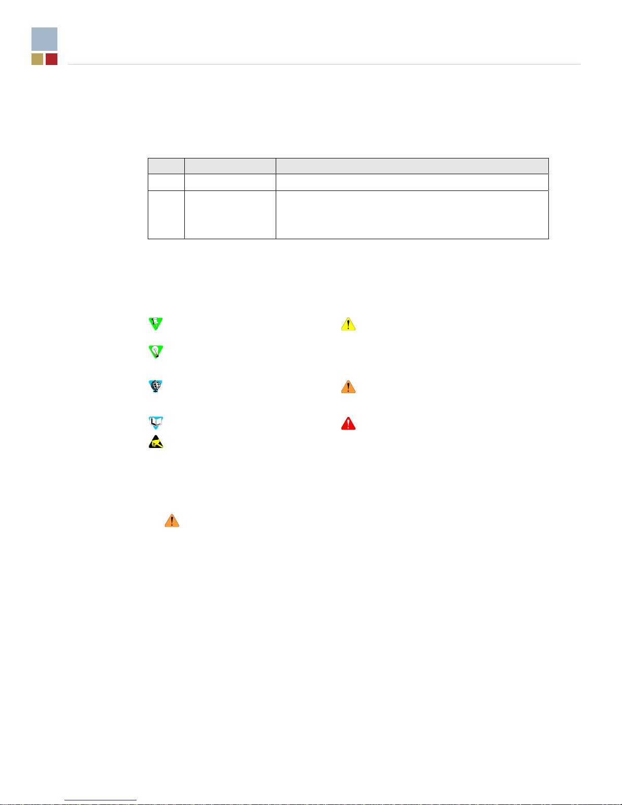
Notational Conventions
This manual uses the following conventions:
• Screen text and syntax strings appear in this font.
• All numbers are decimal unless otherwise stated.
Notes indicate important information
about the product.
Tips indicate alternate techniques or
procedures that you can use to save
time or better understand the product.
Cautions indicate potentially hazardous
situations which, if not avoided, may result
in minor or moderate injury or damage to
data or hardware. It may also alert you
about unsafe practices.
The globe indicates a World Wide
Web address. Warnings indicate potentially hazardous
situations which, if not avoided, can result
in death or serious injury.
The book indicates a book or file.
ESD cautions indicate situations that
may cause damage to hardware via
electro-static discharge (ESD).
Danger indicates imminently hazardous
situations which, if not avoided, will result
in death or serious injury.
Installation Notes
When installing this motherboard into a suitable chassis, refer to the following notes:
• Read and save all instructions.
• Always disconnect Cord/Plug before installation or upgrade. Parts of the motherboard can
remain powered even when the power supply is switched off unless the cord is disconnected.
• Pay attention to the safety warnings included in this document.
• When installing expansion cards, pay attention to the maximum loads detailed in this
document. Use only UL approved peripheral cards.
• Route wiring away from sharp edges, heat sources and cooling fans.
• Pay attention to the thermal issues described in this document. The motherboard requires
suitable airflow to maintain an ambient temperature within its operating range.

KP915GV Product Manual
4
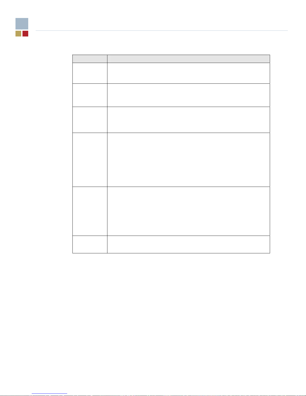
Safety and Approval Notices
Safety and approval notices
Item Description
Battery
This product contains a lithium cell.
• When removing or replacing the lithium cell, do not use a
conductive instrument as a short-circuit may cause the cell
to explode. Always replace the cell with one of the same
type. This product uses a CR2032 cell. Dispose of a spent
cell promptly – do not recharge, disassemble or incinerate.
Keep cells away from children.
• CAUTION! Danger of explosion if battery is incorrectly
replaced. Replace only with the same or equivalent type
recommended by the manufacturer. Dispose of batteries
according to the manufacturer's instructions.
LAN (Local Area
Network) Connector This product may include an RJ45 LAN connector (see
product options). Do not connect to anything other than an
Ethernet LAN.
Thermal Interface
Material This product may contain thermal interface material between
devices and heatsinks. This can cause irritation and can stain
clothing. Avoid prolonged or repeated contact with the skin
and wash thoroughly with soap and water after handling. Avoid
contact with eyes and inhalation of fumes. Do not ingest.
Anti-static
Precautions This product contains static-sensitive components and should
be handled with care. It is recommended that the product be
handled in a Special Handling Area (SHA) as defined in
EN100015-1:1992. Such an area has working surfaces, floor
coverings and chairs connected to a common earth reference
point. An earthed wrist strap should be worn whilst handling.
Other examples of static-sensitive devices are the memory
modules and the processor. Failure to employ adequate anti-
static measures can cause irreparable damage to components
on the motherboard.
Electromagnetic
Compatibility This product is designed to meet the following EMC standards
when installed in a suitable chassis.
• FCC Class B (Title 47 of Code of Federal Regulations,
parts 2 & 15, subpart B)
• EN55022 Class B
• EN55024
Safety This product complies with the American Safety Standard
UL60950 when installed in a suitable chassis.
Legal Directives This product complies with the relevant clauses of the
following European Directives.
Low Voltage Directive 73/23/EEC
EMC Directive 89/336/EEC

KP915GV Product Manual
5
Contents
1OVERVIEW ................................................................................................................10
1.1 Accessories ………………………………………………………………………………………….. 11
1.2 Motherboard Layout ................................................................................................................12
1.3 Block Diagram.........................................................................................................................14
1.4 Configuration ………………………………………………………………………………………….15
1.4.1 Operation Mode Selection Jumper (JP3) ................................................................................15
1.4.2 BIOS Boot Block Write Protection Jumper (JP2).....................................................................16
1.4.3 Clear CMOS Jumper (JP1) .....................................................................................................16
1.4.4 Front Panel Connections.........................................................................................................16
1.4.5 Alternate Power LED...............................................................................................................17
1.5 Installation of CPU ..................................................................................................................17
2MOTHERBOARD DESCRIPTION.............................................................................24
2.1 Processor Support ..................................................................................................................24
2.2 System Clocks ........................................................................................................................24
2.3 On board Clocking Block Diagram ..........................................................................................25
2.4 Mechanical ……………………………………………………………………………………………25
2.5 Expansion Slot Types .............................................................................................................25
2.6 915GV Chipset Feature ..........................................................................................................26
2.7 Video .………………………………………………………………………………………………….27
2.8 Disks …………………………………………………………………………………………………..28
2.9 Audio …………………………………………………………………………………………………..28
2.10 Network ……………………………………………………………………………………………….29
2.11 I/O ……………………………………………………………………………………………………...30
2.12 Power Management ................................................................................................................30
2.13 System management ..............................................................................................................30
2.14 Security ………………………………………………………………………………………………..30
2.15 Programmable Controller (PLD)..............................................................................................31
2.16 CMOS RAM and RTC .............................................................................................................31
2.17 Configuration ………………………………………………………………………………………….31
2.18 BIOS …………………………………………………………………………………………………..31
2.19 Operating Systems Support ....................................................................................................32
2.20 Power Supplies .......................................................................................................................32
2.21 Reliability and Environmental..................................................................................................33
2.22 Regulatory Compliance...........................................................................................................34
3SPECIFICATIONS .....................................................................................................35
3.1 Product Basis …………………………………………………………………………………………35
3.2 Non-Core Integrated Sub-systems..........................................................................................35
3.2.1 I/O Controller Hub 6 (ICH6).....................................................................................................35
3.2.2 Flash BIOS..............................................................................................................................38
3.3 Major Sub-systems .................................................................................................................39
3.3.1 Audio Interface........................................................................................................................39
3.3.2 Hardware Management Interface............................................................................................41
3.3.3 Ethernet Interface....................................................................................................................42
3.3.4 Super I/O Interface..................................................................................................................43
3.4 Motherboard Power Consumption...........................................................................................48

KP915GV Product Manual
6
4MOTHERBOARD BIOS.............................................................................................51
4.1 BIOS Features ........................................................................................................................51
4.2 Post and Boot ………………………………………………………………………………………..51
4.2.1 Hotkeys ...................................................................................................................................52
4.3 Setup Utility ………………………………………………………………………………………….. 52
4.3.1 Enter Setup .............................................................................................................................52
4.3.2 Configuration Reset ................................................................................................................52
4.3.3 Keyboard Command ...............................................................................................................52
4.3.4 Setup Configuration ................................................................................................................53
4.4 Power Management ................................................................................................................93
4.4.1 ACPI Wake-up Support...........................................................................................................93
4.5 Hardware Monitor and Auto Fan Control.................................................................................93
4.5.1 Hardware Monitor....................................................................................................................93
4.5.2 Automatic Fan Control ............................................................................................................93
4.6 Power LED ……………………………………………………………………………………………93
4.7 CPLD …………………………………………………………………………………………………. 94
4.7.1 POST Code Display ................................................................................................................94
4.7.2 BIOS Protection ......................................................................................................................94
4.7.3 LAN Controller.........................................................................................................................94
4.8 TPM ……………………………………………………………………………………………………94
4.9 Normal, Configure and Recovery Mode ..................................................................................94
4.9.1 Normal Mode ..........................................................................................................................95
4.9.2 Configure Mode.......................................................................................................................95
4.9.3 Recovery Mode.......................................................................................................................95
4.10 Update and Recovery Diskette ...............................................................................................95
4.10.1 Update Diskette.......................................................................................................................95
4.10.2 Recovery Diskette...................................................................................................................95
4.11 Tamper Detection....................................................................................................................95
4.12 OEM Features.........................................................................................................................95
4.12.1 POST Logo Change................................................................................................................95
4.12.2 CMOS Default Change ...........................................................................................................96
4.13 PXE ……………………………………………………………………………………………………96
4.14 BIOS Flash Usage Map ..........................................................................................................97
4.15 Processor Microcode Support.................................................................................................97
4.16 SMBIOS ……………………………………………………………………………………………… 97
4.17 Post Code Technical Description ..........................................................................................102
4.18 POST Beep ………………………………………………………………………………………….104
4.19 SMBus Device Configuration ................................................................................................104
5CUSTOMER SUPPORT...........................................................................................105
ATECHNICAL REFERENCE......................................................................................106
A.1 I/O Map ………………………………………………………………………………………………106
A.2 PCI Interrupt Allocation .........................................................................................................107
A.3 PCI Device Assignments.......................................................................................................108
A.4 SMBus Resource Allocation..................................................................................................108
A.5 ISA Interrupt Allocation .........................................................................................................109
A.6 ISA DMA Channel Allocation ................................................................................................109
A.7 BIOS Organization ................................................................................................................110

KP915GV Product Manual
7
BCONTROL REGISTERS..........................................................................................111
B.1 Index Register .......................................................................................................................111
B.2 Watchdog Control .................................................................................................................111
B.3 Watchdog Kick ......................................................................................................................112
B.4 Watchdog Status...................................................................................................................112
B.5 Watchdog Timeout Period.....................................................................................................113
B.6 General Purpose I/O Port 1...................................................................................................113
B.7 General Purpose I/O Port 2 and Control ...............................................................................113
B.8 PWM Control ………………………………………………………………………………………..114
B.9 Processor Identification.........................................................................................................114
B.10 Controller Part Number .........................................................................................................115
CCONNECTOR DESCRIPTIONS ..............................................................................116
C.1 Connector Part Numbers ......................................................................................................116
C.2 PCI-E Expansion Slot (ADD2 card mode).............................................................................117
C.3 PCI Expansion Slot ...............................................................................................................118
C.4 PCI Express x1 Slot ..............................................................................................................119

KP915GV Product Manual
8
Figures
Figure 1. KP915GV Board Layout.............................................................................................12
Figure 2. KP915GV Block diagram ...........................................................................................14
Figure 3. Jumpers .....................................................................................................................15
Figure 4. Clocking Block Diagram .............................................................................................25
Figure 5. KP915GV Board Slot Layout......................................................................................28
Figure 6. Audio Jack Socket and ATAPI Connectors ................................................................29
Figure 7. SST 49LF004B Functional Block Diagram.................................................................38
Figure 8. SigmaTel STAC9200 High Definition Block Diagram .................................................40
Figure 9. NS LM96000CIM Block Diagram ...............................................................................41
Figure 10. PC8374K Block Diagram ...........................................................................................43
Figure 11. BIOS ROM Addresses .............................................................................................110
Tables
Revision history .................................................................................................................................3
Safety and approval notices ..............................................................................................................4
Product Specification Overview .......................................................................................................10
Table 1. KP915GV Motherboard ...................................................................................................26
Table 3. ACPI Power States ..........................................................................................................30
Table 4. Power Supply Connector .................................................................................................32
Table 5. Environmental Specifications...........................................................................................33
Table 6. Regulatory Testing* .........................................................................................................34
Table 7. References ....................................................................................................................105
Table 8. I/O Map..........................................................................................................................106
Table 9. PCI Interrupt Allocation..................................................................................................107
Table 10. PCI Device Assignments .............................................................................................108
Table 11. SMBus Resource Allocation ........................................................................................108
Table 12. ISA Interrupt Allocation ................................................................................................109
Table 13. ISA DMA Channel Allocation .......................................................................................109
Table 14. Connector part numbers ..............................................................................................116
Table 15. ADD2 Expansion Slot ..................................................................................................117
Table 16. PCI Expansion Slot......................................................................................................118
Table 17. PCI Express x1 Slot (PCI-E x1) ...................................................................................119
Table 18. P/S2 Mouse and P/S2 Keyboard .................................................................................119
Table 20. Serial Port....................................................................................................................120
Table 21. VGA Port .....................................................................................................................120
Table 22. 2 x Dual Stack USB Ports............................................................................................120
Table 24. 3 x Audio Jack .............................................................................................................121
Table 25. 1394 Header................................................................................................................121
Table 26. Front Panel Header .....................................................................................................121
Table 27. General Purpose I/O Headers ......................................................................................122
Table 28. Power Supply Connector .............................................................................................122
Table 29. Floppy Disk Connector ................................................................................................122
Table 30. ATA/100 Hard Drive Disk Connector ...........................................................................123
Table 32. 3X Internal Audio Headers...........................................................................................123
Table 33. TPM Header ...............................................................................................................124

KP915GV Product Manual
9
Table 34. Complex Programmable Logic Device (CPLD) JTAG Header....................................124
Table 35. Serial Port 2 Header ...................................................................................................124
Table 36. 4 X Internal USB Headers ...........................................................................................124
Table 37. Remote Thermal Sensor..............................................................................................125
Table 38. 3 X Fan Connector.......................................................................................................125
Table 39. SMBus Connector........................................................................................................125
Table 40. PS/2 Keyboard Header................................................................................................125
Table 41. PS/2 Mouse Header ....................................................................................................125

KP915GV Product Manual
10
1 Overview
Target applications are transaction terminals, medical, test & measurement, gaming, industrial
automation applications and other enterprise systems. This motherboard is part of the RadiSys
Endura product line, which is specifically targeted at embedded applications with a lifetime of 5
years. Products are fully revision controlled and any change to form, fit or function will be notified to
customers in advance via a Product Change Notification procedure.
Product Specification Overview
Item Description
Form Factor ATX 12” x 9.6”, 6 expansion slots
Processor Support for an Intel® Pentium® 4 or Celeron D processor in a LGA775 socket
with an 800MHz or 533MHz FSB
Embedded processor requirements:
Intel® Pentium® 4 Processor 551 (3.4GHz 800MHz FSB 1MB L2)
Intel® Celeron™ D Processor 341 (2.93GHz 533MHz FSB 256KB L2)
Chipset Intel 915GV GMCH and Intel ICH6 I/O hub
Memory Four DIMM sockets for DDR2 400/533 modules
Video Intel® GMA900 video controller integrated within chipset
Audio Two channel stereo audio using the Sigmatel STAC9200 audio controller with
Intel HD Audio interface operation option
Two plug and play jacks on I/O panel (default MIC, line-out)
Three ATAPI connectors – line input, line output, and microphone input
On-board PC speaker (beep)
Expansion
Capabilities 915GV ATX Three PCI, two x1 PCI-E, one ADD2 slots
(No PCI riser extension connector)
Power
Management ACPI 2.0 supporting states S0, S3, S4, S5, and C0, C1, C2, C3
System
Management Voltage, temperature and fan monitoring (3 fans)
Lithium cell voltage monitoring
Automatic fan speed control (3 fans)
Programmable watchdog timer
SMBus header
Security Header for TPM 1.1 compliant module
BIOS Phoenix Award BIOS for the Intel 915G/GV chipset
Includes video BIOS and network boot
4Mbit Firmware Hub
Build option for socketed BIOS with write-protect jumper (enabled by the PLD
logic)
User defined BIOS default settings
I/O Eight USB 2.0 ports - four on I/O panel and four on locking headers
General purpose I/O lines (13) with LCD character display support
Firewire Available with IEEE 1394b function with single port via an on-board header
connector (based on TI TSB82AA2 controller and TSB81BA3 transceiver)
KP915GV Product Manual
11
Product Specification Overview
Item Description
Network Intel 82573V (or ‘L) PCI-E Gbit Ethernet controller, co-lay with Intel 82562GZ
10/100 PHY (using the integrated MAC)
Available with second Intel 82573V (or ‘L) Gbit Ethernet controller
Disks Four SATA ports with locking headers
Single Ultra ATA/100 interface supporting hard disks and ATAPI drives
One FDD interface
Super I/O &
H/W Monitor Nat Semiconductor PC8374K Super I/O and Nat Semiconductor LM9600
hardware monitoring device
Automatic fan speed control based on thermal monitoring (note that the BIOS
Setup is used for configuration and status information)
Header
Connectors GPIO 2 x 10 pin with housing
SMbus 1 x 4 pin with housing
COM2 2 x 5 pin with housing
Kbd/Mouse 1 x 4 pin with housing
Remote thermal sensor 1 x 2 pin with housing
FDD 1 x FDD connector
1394b 2 x 5 pin connector
I/O Panel PS/2 keyboard and mouse
Analog VGA
Bi-directional/EPP/ECP parallel port
COM1 RS232
One or two dual USB + RJ45 stacks
Audio jack stack (2 jacks)
RadiSys PLD Lattice LC4128ZC-75TN100C PLD for watchdog, GPIO, BIOS write-protect
support
1.1 Accessories
There are two I/O shields, one for the single Ethernet configuration and one for the dual Ethernet
configuration, and an available fan heat sink for the processor. These are separately orderable
product codes.
ATX-L KP IOSHLD ATX I/O Shield for KP915GV

KP915GV Product Manual
12
1.2 Motherboard Layout
Figure 1 shows the layout of the KP915GV motherboard with the major components identified.
Figure 1. KP915GV Board Layout
6
7
8
9
1
2
3
4
5
10
11
12
13 14 15 16 17 18 19 20 21 22 23 24 25
35
37
36
39
38
41
40
43
42
2726 28 29 30 31
45
44
53545859
(Optional)
57 56
46
4748
34
33
32
4950515255

KP915GV Product Manual
13
Component Identification
Description Description Description
1 Super IO 21 Ethernet port 1
(option) 41 USB port 2 header
2 Memory sockets 22 I/O panel USB port 7 42 USB port 3 header
3 Serial port 2 header 23 I/O panel USB port 8 43 USB port 4 header
4 Remote thermal sensor 24 Microphone input jack 44 SMBus header
5 CPU FAN power
connector
25 Audio line output jack 45 BIOS ROM write-
protect jumper
6 Chipset GMCH 26 Ethernet controller 1
(option)
46 Clear CMOS Jumper
7 775-pin socket for
processor
27 ADD2 slot 47 GPIO header
8 Clock generator 28 Ethernet controller 2 48 BIOS ROM (FWH)
9 System fan power
connector
29 PCI Express x1 slot 49 CPLD control logic
10 PS/2 mouse header 30 PCI slot 2.3 50 JTAG header
11 PS/2 keyboard header 31 HD Audio CODEC 51 I/O controller hub
(ICH6)
12 12V power connector 32 Stereo audio (CD) line
input header
52 Operation Mode
Jumper
13 PS/2 mouse (green) 33 Stereo audio
(microphone) input
header
53 Front panel header
14 PS/2 keyboard (purple) 34 Stereo audio line
output header
54 SATA connectors
15 Serial port 35 Buzzer 55 Chassis fan power
connector
16 Parallel port 36 1394 controller 56 Primary power supply
connector
17 VGA monitor 37 RTC battery 57 IDE connector
18 Ethernet port 2 38 1394 PHY
(TSB81BA3I)
58 TPM header
19 I/O panel USB port 5 39 1394 header 59 FDD connector
20 I/O panel USB port 6 40 USB port 1 header

KP915GV Product Manual
14
1.3 Block Diagram
Figure 2 shows the block diagram of the KP915GV motherboard.
Figure 2. KP915GV Block diagram
DIMM2
DIMM4
Channel B DDR-2
400/533MHz
Channel A DDR-2
Serial Port2
Serial Port1
Keyboard
NS PC8374
K
SUPER I/O
FWH Flash
BIOS
Floppy
Mouse
Parallel
A
zalia Codec
USB2.0
USB2.0
LPC
STAC9200
High Definition Audio
Intel 82562G
Z
LAN-Lin
k
PCIE x1 Interface Intel 82573
E
SAT
A
Port 3
Port 2
Port 1
Serial AT
A
Serial AT
A
Serial AT
A
SAT
A
SAT
A
SAT
A
CRT
Port 4
Serial AT
A
VG
A
A
T
A
I/O Panel
USB2.0 Port
5
USB2.0 Port1
USB2.0 Port
3
USB2.0 Port
2
Header
L
GA775 processor
P
entium 4 EE
PC
I
-
E
Slot
2
4 Lanes
ICH6
PCI Interface
P
rescott, Tejas
USB2.0 Port
8
GMCH
V
RD 10.1
PCI Interface 1394
TSB82AA2
I
CK-410 Clock
PCIEx16 Por
t
USB2.0 Port
6
IDE CONN 1
PCI Slot 1,2&
3
A
TX Form Facto
r
USB2.0 Port
7
PC
I
-
E
Slot 1
Direct Media Interface (DMI)
4 Phase PW
M
800/533 FSB
PCIE x1 Interface
A
TA100
S
ocket T
USB2.0 Port4
4
Mb
Intel SDVO Car
d
Channel A DDR-2
DIMM1
DIMM3
400/533MHz
G
rantsdale
Channel B DDR-2
KP915GV Product Manual
15
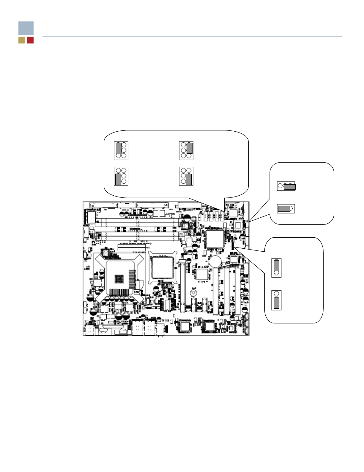
1.4 Configuration
The majority of the configuration of the motherboard is done through the Setup utility built into the
BIOS – discussed later in this document. There are, however, a number of jumpers that control the
operation of the motherboard as described below. Some jumpers are not fitted to certain products.
Figure 3. Jumpers
1.4.1 Operation Mode Selection Jumper (JP3)
This jumper selects one of the following operating modes for the motherboard (pins 1, 3, 5) and
controls write capability for the CPLD content (pins 2, 4, 6).
Normal Mode (Jumper between pins 1 & 3) This is the factory default position the jumper
should be in for normal operation of the motherboard.
Configure Mode (Jumper between pins 3 & 5) With the jumper in this position the motherboard
automatically runs the BIOS Setup utility regardless of the state of the Setup
disable flag that can be set in the BIOS defaults. In this mode, the CMOS RAM
contents are ignored and the defaults are used to configure the motherboard.
JP2
BIOS Unlock
1
BIOS Lock
(No jumper = Unlock)
1(No jumper = Recover) JP3 (No jumper = Protected)
Normal CPLD Write Enable
Configure CPLD Write
Protected
1 JP1
Clear CMOS
Normal
(No jumper = Normal)

KP915GV Product Manual
16
Recover Mode (No jumper) With no jumper installed on pins 1, 3, and 5 recovery mode is entered.
The motherboard does not boot and waits until a valid recovery diskette is
detected and then copies new BIOS into the ROM. The motherboard must be
powered down and then re-powered with the jumper in the normal position before
normal operation can resume.
CPLD Write Enabled (Jumper between pins 2 & 4) In this position the contents of the CPLD can
be reprogrammed.
CPLD Write Protected (Jumper between pins 4 & 6) This is the factory default position. In this
position, or with no jumper on pins 2, 4, and 6, the contents of the CPLD are
protected from reprogramming.
1.4.2 BIOS Boot Block Write Protection Jumper (JP2)
(Jumper between pins 1 & 2) This is the factory default position. A jumper installed in this position.
or no jumper installed, enables changes to contents of BIOS ROM boot block (unlocked position).
Some motherboard applications may want to have boot block write-protected BIOS. This can be
provided via the BIOS boot block write protection jumper. If a jumper is installed between pins 2 &
3 (locked position), the contents of BIOS ROM boot block cannot be changed in any way.
1.4.3 Clear CMOS Jumper (JP1)
(Jumper between pins 2 & 3) This is the factory default position. Either this position or no jumper
installed, is the normal operating configuration. Installing a jumper between pins 1 & 2 clears
(resets) the CMOS.
1.4.4 Front Panel Connections
The primary controls and indicators for the motherboard are connected via the front panel
connector using either a single ribbon cable to a ‘front panel’ assembly, or using a number of small
PC-standard connectors. The functions are described below. See appendix B for the connector pin-
out information.
Power LED
Connects either a single-color LED (usually green) or a two-terminal bi-color LED (usually
green/yellow) to indicate the powered status of the motherboard. In both cases, the ‘green’ anode
should be attached to pin 2 of the front panel connector. Refer to the Enhanced Power
Management LED portion in section 3.3.4.4 of this document for further information.
Power Switch
If the motherboard is used with a soft-switch power supply, a momentary switch should be
connected between pins 6 and 8 of the power switch connections on the front panel connector. If
the switch is closed for greater than approximately 4 seconds, the motherboard powers off
immediately, regardless of the state of the operating system, losing any system context information.
This input is redundant when using a hard-switch power supply.
Reset Switch
If used, a momentary switch connected between pins 5 and 7 will cause the motherboard to restart
when closed.
Hard Disk LED
To indicate hard disk activity on either of the two ATA channels, a single color LED should be
connected between pins 1 (anode) and 3.
Speaker
Connect an external speaker between pins 10 and 12 or 10 and 16. This is used only for the PC
‘beep’ functions. The speaker should typically be 8Ω.

KP915GV Product Manual
17
Tamper Switch
To make use of the tamper detection logic of the motherboard, connect a momentary switch
between pins 18 and 20. The switch should be open when the chassis is closed.
1.4.5 Alternate Power LED
The power LED function on the front panel connector is duplicated on the Alternate Power LED
connector for use with LEDs cabled to a 3-pin connector. Do not use both the primary (front panel)
and alternate connectors simultaneously.
1.5 Installation of CPU
1.5.1 Installation of CPU
Below is the CPU socket illustration. Follow these procedures to install a CPU.
1. Use thumb & forefinger to hold the lifted tab of the cap.
2. Lift the cap up and pick to upload the cap completely from the socket.
Load leve
r
Load Stiffene
r
Load ca
p
Load
p
late
Lifted tab

KP915GV Product Manual
18
3. Use thumb & forefinger to hold the hook of the load lever and pull the lever sideways to unlock it.
Warning:
DO NOT use finger to lift the locking lever, as injury could occur to the finger and the SKT could be
damaged.
4. Lift up the lever. Use thumb to open the load plate. Be careful not to touch the contacts.
5. Hold the CPU and tilt it to some degree since the contacts are designed to be hooked, and
then match the triangle marker to Pin 1 position as shown below. Carefully insert the CPU
into the socket until it fits in place.
Correct Wrong
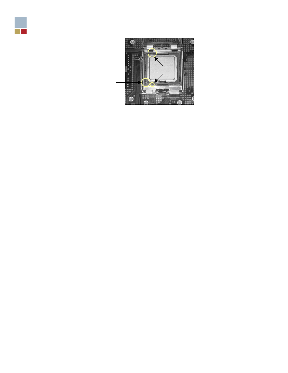
KP915GV Product Manual
19
A
li
g
nment ke
y
Pin 1 indicato
r

KP915GV Product Manual
20
6. Close the load plate, and slightly push down the tongue side.
7. Lower the lever and lock it to the load plate, then the CPU is locked in place.
CAUTION
Excessive temperatures will severely damage the CPU and system. Therefore, you should install
CPU cooling fan and make sure that the cooling fan works normally at all times in order to prevent
overheating and damaging to the CPU. Please refer to your CPU fan user guide to install it
properly.
1.5.2 Installation of Memory
This motherboard includes four 240-pin slots with 1.8V for DDR2. You must install at least one
memory bank to ensure normal operation.
Installation of DDR2 Memory
1. There is only one gap in the middle of the DIMM slot, and the memory module can be fixed in
one direction only. Unlock a DIMM slot by pressing the module clips outward.
2. Align the memory module to the DIMM slot, and insert the module vertically into the DIMM slot.
Slightly push down
the tongue side
Table of contents
Popular Motherboard manuals by other brands

adafruit learning system
adafruit learning system MAX9744 manual

Gigabyte
Gigabyte GA-P85-D3T user manual

ASROCK
ASROCK X99M Extreme4 user manual

Microchip Technology
Microchip Technology PICtail MRF24J40MC user guide

Texas Instruments
Texas Instruments BOOST-LDC3114EVM user guide

Asus
Asus Strix Z270I Gaming quick start guide


