Exar XRT86VX38 User manual

Exar Corporation 48720 Kato Road, Fremont CA, 94538 •(510) 668-7000 •FAX (510) 668-7017 •www.exar.com
XRT86VX38
8-CHANNEL T1/E1/J1 FRAMER/LIU COMBO - T1 REGISTER DESCRIPTION
2011 REV. 1.0.3
GENERAL DESCRIPTION
The XRT86VX38 is an eight-channel 1.544 Mbit/s or
2.048 Mbit/s DS1/E1/J1 framer and Long-haul/Short-
hual LIU integrated solution featuring R3technology
(Relayless, Reconfigurable, Redundancy) and BITS
Timing element. The physical interface is optimized
with internal impedance, and with the patented pad
structure, the XRT86VX38 provides protection from
power failures and hot swapping.
The XRT86VX38 contains an integrated DS1/E1/J1
framer and LIU which provide DS1/E1/J1 framing and
error accumulation in accordance with ANSI/ITU_T
specifications. Each framer has its own framing
synchronizer and transmit-receive slip buffers. The
slip buffers can be independently enabled or disabled
as required and can be configured to frame to the
common DS1/E1/J1 signal formats.
Each Framer block contains its own Transmit and
Receive T1/E1/J1 Framing function. There are 3
Transmit HDLC controllers per channel which
encapsulate contents of the Transmit HDLC buffers
into LAPD Message frames. There are 3 Receive
HDLC controllers per channel which extract the
payload content of Receive LAPD Message frames
from the incoming T1/E1/J1 data stream and write the
contents into the Receive HDLC buffers. Each framer
also contains a Transmit and Overhead Data Input
port, which permits Data Link Terminal Equipment
direct access to the outbound T1/E1/J1 frames.
Likewise, a Receive Overhead output data port
permits Data Link Terminal Equipment direct access
to the Data Link bits of the inbound T1/E1/J1 frames.
The XRT86VX38 fully meets all of the latest T1/E1/J1
specifications: ANSI T1/E1.107-1988, ANSI T1/
E1.403-1995, ANSI T1/E1.231-1993, ANSI T1/
E1.408-1990, AT&T TR 62411 (12-90) TR54016, and
ITU G-703, G.704, G706 and G.733, AT&T Pub.
43801, and ETS 300 011, 300 233, JT G.703, JT
G.704, JT G706, I.431. Extensive test and diagnostic
functions include Loop-backs, Boundary scan,
Pseudo Random bit sequence (PRBS) test pattern
generation, Performance Monitor, Bit Error Rate
(BER) meter, forced error insertion, and LAPD
unchannelized data payload processing according to
ITU-T standard Q.921.
.
APPLICATIONS AND FEATURES (NEXT PAGE)
FIGURE 1. XRT86VX38 EIGHT CHANNEL DS1 (T1/E1/J1) FRAMER/LIU COMBO
Performance
Monitor
PRBS
Generator &
Analyser
HDLC/LAPD
Controllers
LIU &
Loopback
Control
DMA
Interface
Signaling &
Alarms JTAG
WR
ALE_AS
RD
RDY_DTACK
P
Select
A[11:0]D[7:0]
Microprocessor
Interface
4
3
Tx Serial
Clock
Rx Serial
Clock
8kHz sync
OSC
Back Plane
1.544-16.384 Mbit/s
Local PCM
Highway
ST-BUS
2-Frame
Slip Buffer
Elastic Store
Tx Serial
Data In Tx LIU
Interface
2-Frame
Slip Buffer
Elastic Store
Rx LIU
Interface
Rx Framer
Rx Serial
Data Out
RTIP
RRING
TTIP
TRING
External Data
Link Controller
Tx Overhead In Rx Overhead Out
XRT86VX38
Tx Framer
LLB LB
System (Terminal) Side
Line Side
1:1 Turns Ratio
1:2 Turns Ratio
Memory Intel/Motorola µP
Configuration, Control &
Status Monitor
RxLOS
TxON
INT

XRT86VX38
2
8-CHANNEL T1/E1/J1 FRAMER/LIU COMBO - T1 REGISTER DESCRIPTION REV. 1.0.3
APPLICATIONS
High-Density T1/E1/J1 interfaces for Multiplexers, Switches, LAN Routers and Digital Modems
SONET/SDH terminal or Add/Drop multiplexers (ADMs)
T1/E1/J1 add/drop multiplexers (MUX)
Channel Service Units (CSUs): T1/E1/J1 and Fractional T1/E1/J1
BITS Timing
Digital Access Cross-connect System (DACs)
Digital Cross-connect Systems (DCS)
Frame Relay Switches and Access Devices (FRADS)
ISDN Primary Rate Interfaces (PRA)
PBXs and PCM channel bank
T3 channelized access concentrators and M13 MUX
Wireless base stations
ATM equipment with integrated DS1 interfaces
Multichannel DS1 Test Equipment
T1/E1/J1 Performance Monitoring
Voice over packet gateways
Routers
FEATURES
Supports Section 13 - Synchronization Interface in ITU G.703 for both Transmit and Receive Paths
Supports SSM Synchronous Messaging Generation (BOC for T1, National Bits for E1) on the Transmit Path
Supports SSM Synchronous Messaging Extraction (BOC for T1, National Bits for E1) on the Receive Path
Supports BITS timing generation on the Transmit Outputs
Supports BITS timing extraction from NRZ data on the Analog Receive Path
DS-0 Monitoring on both Transmit and Receive Time Slots
Supports SSM Synchronization Messaging per ANSI T1.101-1999 and ITU G.704
Supports a Customized Section 13 - Synchronization Interface in G.703 at 1.544MHz
Independent, full duplex DS1 Tx and Rx Framer/LIUs
Each channel has full featured Long-haul/Short-haul LIU
Two 512-bit (two-frame) elastic store, PCM frame slip buffers (FIFO) on TX and Rx provide up to 8.192 MHz
asynchronous back plane connections with jitter and wander attenuation
Supports input PCM and signaling data at 1.544, 2.048, 4.096 and 8.192 Mbits. Also supports 2-channel
multiplexed 12.352/16.384 (HMVIP/H.100) Mbit/s on the back plane bus
Programmable output clocks for Fractional T1/E1/J1
Supports Channel Associated Signaling (CAS)
Supports Common Channel Signalling (CCS)
Supports ISDN Primary Rate Interface (ISDN PRI) signaling
XRT86VX38
3
REV. 1.0.3 8-CHANNEL T1/E1/J1 FRAMER/LIU COMBO - T1 REGISTER DESCRIPTION 8-CHANNEL T1/E1/J1 FRAMER/
Extracts and inserts robbed bit signaling (RBS)
3 Integrated HDLC controllers for transmit and receive, each controller having two 96-byte buffers (buffer 0 /
buffer 1)
HDLC Controllers Support SS7
Timeslot assignable HDLC
V5.1 or V5.2 Interface
Automatic Performance Report Generation (PMON Status) can be inserted into the transmit LAPD interface
every 1 second or for a single transmission
Supports SPRM and NPRM
Alarm Indication Signal with Customer Installation signature (AIS-CI)
Remote Alarm Indication with Customer Installation (RAI-CI)
Gapped Clock interface mode for Transmit and Receive.
Intel/Motorola and Power PC interfaces for configuration, control and status monitoring
Parallel search algorithm for fast frame synchronization
Wide choice of T1 framing structures: SF/D4, ESF, SLC®96, T1DM and N-Frame (non-signaling)
Direct access to D and E channels for fast transmission of data link information
Full BERT Controller for generation and detection on system and line side of the chip
PRBS, QRSS, and Network Loop Code generation and detection
Seven Independent, simultaneous Loop Code Detectors per Channel
Programmable Interrupt output pin
Supports programmed I/O and DMA modes of Read-Write access
The framer block encodes and decodes the T1/E1/J1 Frame serial data
Detects and forces Red (SAI), Yellow (RAI) and Blue (AIS) Alarms
Detects OOF, LOF, LOS errors and COFA conditions
Loopbacks: Local (LLB) and Line remote (LB)
Facilitates Inverse Multiplexing for ATM
Performance monitor with one second polling
Boundary scan (IEEE 1149.1) JTAG test port
Accepts external 8kHz Sync reference
1.8V Inner Core
3.3V CMOS operation with 5V tolerant inputs
256-pin fpBGA and 329-pin fpBGA package with -40C to +85Coperation
ORDERING INFORMATION
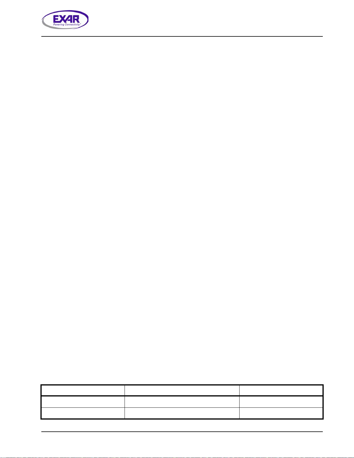
PART NUMBER PACKAGE OPERATING TEMPERATURE RANGE
XRT86VX38IB256 256 PIn Fine Pitch Ball Grid Array -40C to +85C
XRT86VX38IB329 329 PIn Fine Pitch Ball Grid Array -40C to +85C

XRT86VX38
I
8-CHANNEL T1/E1/J1 FRAMER/LIU COMBO - T1 REGISTER DESCRIPTION REV. 1.0.3
LIST OF TABLES
Table 1:: Register Summary ..............................................................................................................................................4
Table 2:: Clock Select Register(CSR) Hex Address: 0xN100 ........11
Table 3:: Line Interface Control Register (LICR) Hex Address: 0xN101 ...............13
Table 4:: General Purpose Input/Output 0 Control Register(GPIOCR0) Hex Address: 0x0102 ...........................15
Table 5:: General Purpose Input/Output 1 Control Register(GPIOCR1) Hex Address: 0x4102 ........................16
Table 6:: Framing Select Register (FSR) Hex Address: 0xN107 ....................17
Table 7:: Alarm Generation Register (AGR) Hex Address: 0xN108 .....................19
Table 8:: yellow alarm duration and format when one second rule is not enforced .........................................................20
Table 9:: yellow alarm format when one second rule is enforced ....................................................................................21
Table 10:: Synchronization MUX Register (SMR) Hex Address: 0xN109 .................23
Table 11:: Transmit Signaling and Data Link Select Register (TSDLSR) Hex Address:0xN10A ..................26
Table 12:: Framing Control Register (FCR) Hex Address: 0xN10B ..................28
Table 13:: Receive Signaling & Data Link Select Register (RSDLSR) Hex Address: 0xN10C ....................29
Table 14:: Receive Signaling Change Register 0 (RSCR 0) Hex Address: 0xN10D ..........31
Table 15:: Receive Signaling Change Register 1(RSCR 1) Hex Address: 0xN10E ......31
Table 16:: Receive Signaling Change Register 2 (RSCR 2) Hex Address: 0xN10F ........31
Table 17:: Receive In Frame Register (RIFR) Hex Address: 0xN112 ..................32
Table 18:: Data Link Control Register (DLCR1) Hex Address: 0xN113 ....................33
Table 19:: Transmit Data Link Byte Count Register (TDLBCR1) Hex Address: 0xN114 ....................35
Table 20:: Receive Data Link Byte Count Register (RDLBCR1) Hex Address: 0xN115 ..................36
Table 21:: Slip Buffer Control Register (SBCR) Hex Address: 0xN116 .....................37
Table 22:: FIFO Latency Register (FFOLR) Hex Address: 0xN117 ................38
Table 23:: DMA 0 (Write) Configuration Register (D0WCR) Hex Address: 0xN118 ..................39
Table 24:: DMA 1 (Read) Configuration Register (D1RCR) Hex Address: 0xN119 .................40
Table 25:: Interrupt Control Register (ICR) Hex Address: 0xN11A ......................41
Table 26:: LAPD Select Register (LAPDSR) Hex Address: 0xN11B ................42
Table 27:: Customer Installation Alarm Generation Register (CIAGR) Hex Address: 0xN11C .......................43
Table 28:: Performance Report Control Register (PRCR) Hex Address: 0xN11D ....................44
Table 29:: Gapped Clock Control Register (GCCR) Hex Address: 0xN11E ..................45
Table 30:: Transmit Interface Control Register (TICR) Hex Address:0xN120 ....................46
Table 31:: Transmit Interface Speed When Multiplexed Mode is Disabled (TxMUXEN = 0) ...........................................48
Table 32:: Transmit Interface Speed when Multiplexed Mode is Enabled (TxMUXEN = 1) ............................................49
Table 33:: BERT Control & Status Register (BERTCSR0) Hex Address: 0xN121 ...............50
Table 34:: Receive Interface Control Register (RICR) Hex Address: 0xN122 ...............52
Table 35:: Receive Interface Speed When Multiplexed Mode is Disabled (TxMUXEN = 0) ............................................54
Table 36:: Receive Interface Speed when Multiplexed Mode is Enabled (TxMUXEN = 1) .............................................55
Table 37:: BERT Control & Status Register (BERTCSR1) Hex Address: 0xN123 .....................56
Table 38:: Loopback Code Control Register - Code 0 (LCCR0) Hex Address: 0xN124 ...............58
Table 39:: Transmit Loopback Coder Register (TLCR) Hex Address: 0xN125 .............60
Table 40:: Receive Loopback Activation Code Register - Code 0 (RLACR0) Hex Address: 0xN126 ................60
Table 41:: Receive Loopback Deactivation Code Register - Code 0 (RLDCR0) Hex Address: 0xN127 .................60
Table 42:: Receive LoopCode Detection Switch (RLCDS) Hex Address: 0xN128 ..................................61
Table 43:: Defect Detection Enable Register (DDER) Hex Address: 0xN129 ..............62
Table 44:: Loopback Code Control Register - Code 1 (LCCR1) Hex Address: 0xN12A ........................63
Table 45:: Receive Loopback Activation Code Register - Code 1 (RLACR1) Hex Address: 0xN12B ..................64
Table 46:: Receive Loopback Deactivation Code Register - Code 1 (RLDCR1) Hex Address: 0xN12C ....................64
Table 47:: Loopback Code Control Register - Code 2 (LCCR2) Hex Address: 0xN12D ........................65
Table 48:: Receive Loopback Activation Code Register - Code 2 (RLACR2) Hex Address: 0xN12E ..................66
Table 49:: Receive Loopback Deactivation Code Register - Code 2 (RLDCR2) Hex Address: 0xN12F .....................66
Table 50:: Transmit LoopCode Generation Switch (TLCGS) Hex Address: 0xN140 ...............................67
Table 51:: LoopCode Timer Select (LCTS) Hex Address: 0xN141 ..........................................................67
Table 52:: Transmit SPRM and NPRM Control Register (TSPRMCR) Hex Address: 0xN142 ................67
Table 53:: Data Link Control Register (DLCR2) Hex Address: 0xN143 ...................69
Table 54:: Transmit Data Link Byte Count Register (TDLBCR2) Hex Address: 0xN144 ...................71
Table 55:: Receive Data Link Byte Count Register (RDLBCR2) Hex Address: 0xN145 .................72
Table 56:: Loopback Code Control Register - Code 3 (LCCR3) Hex Address: 0xN146 .........................73
Table 57:: Receive Loopback Activation Code Register - Code 3 (RLACR3) Hex Address: 0xN147 ..................74
Table 58:: Receive Loopback Deactivation Code Register - Code 3 (RLDCR3) Hex Address: 0xN148 .....................74

XRT86VX38
II
REV. 1.0.3 8-CHANNEL T1/E1/J1 FRAMER/LIU COMBO - T1 REGISTER DESCRIPTION
Table 59:: Loopback Code Control Register - Code 4 (LCCR4) Hex Address: 0xN149 ......................... 75
Table 60:: Receive Loopback Activation Code Register - Code 4 (RLACR4) Hex Address: 0xN14A .................. 76
Table 61:: Receive Loopback Deactivation Code Register - Code 4 (RLDCR4) Hex Address: 0xN14B .................... 76
Table 62:: Loopback Code Control Register - Code 5 (LCCR5) Hex Address: 0xN14C ........................77
Table 63:: Receive Loopback Activation Code Register - Code 5 (RLACR5) Hex Address: 0xN14D .................. 78
Table 64:: Receive Loopback Deactivation Code Register - Code 5 (RLDCR5) Hex Address: 0xN14E .................... 78
Table 65:: Loopback Code Control Register - Code 6 (LCCR6) Hex Address: 0xN14F ........................79
Table 66:: Receive Loopback Activation Code Register - Code 6 (RLACR6) Hex Address: 0xN150 .................. 80
Table 67:: Receive Loopback Deactivation Code Register - Code 6 (RLDCR6) Hex Address: 0xN151 ..................... 80
Table 68:: Data Link Control Register (DLCR3) Hex Address: 0xN153 .................81
Table 69:: Transmit Data Link Byte Count Register (TDLBCR3) Hex Address: 0xN154 ................... 83
Table 70:: Receive Data Link Byte Count Register (RDLBCR3) Hex Address: 0xN155 .................84
Table 71:: Loopback Code Control Register - Code 7 (LCCR7) Hex Address: 0xN156 ......................... 85
Table 72:: Receive Loopback Activation Code Register - Code 7 (RLACR7) Hex Address: 0xN157 .................. 86
Table 73:: Receive Loopback Deactivation Code Register - Code 7 (RLDCR7) Hex Address: 0xN158 ..................... 86
Table 74:: BERT Control Register (BCR) Hex Address: 0xN163 ...............87
Table 75:: T1 SSM Messages .........................................................................................................................................88
Table 76:: SSM BOC Control Register (BOCCR 0xN170h) ............................................................................................89
Table 77:: SSM Receive FDL Register (RFDLR 0xN171h) .............................................................................................90
Table 78:: SSM Receive FDL Match 1 Register (RFDLMR1 0xN172h) ..........................................................................91
Table 79:: SSM Receive FDL Match 2 Register (RFDLMR2 0xN173h) ..........................................................................91
Table 80:: SSM Receive FDL Match 3 Register (RFDLMR3 0xN174h) ..........................................................................91
Table 81:: SSM Transmit FDL Register (TFDLR 0xN175h) ............................................................................................92
Table 82:: SSM Transmit Byte Count Register (TBCR 0xN176h) ...................................................................................92
Table 83:: Receive DS-0 Monitor Registers (RDS0MR) Hex Address:
0xN160 to 0xN16F (not including 0xN163) and 0xN1C0 to 0xN1D0 ................................................................93
Table 84:: Transmit DS-0 Monitor Registers (TDS0MR) Hex Address: 0xN1D1 to 0xN1F0 .......................................93
Table 85:: Device ID Register (DEVID) Hex Address: 0x01FE ...........94
Table 86:: Revision ID Register (REVID) Hex Address: 0x01FF ...........94
Table 87:: Transmit Channel Control Register 0-23 (TCCR 0-23) Hex Address: 0xN300 to 0xN317 ................... 95
Table 88:: Transmit User Code Register 0-23 (TUCR 0-23) Hex Address: 0xN320 to 0xN337 ...............97
Table 89:: Transmit Signaling Control Register 0-23 (TSCR 0-23) Hex Address: 0xN340 to 0xN357 ...................... 98
Table 90:: Receive Channel Control Register 0-23 (RCCR 0-23) Hex Address: 0xN360 to 0xN377 ................100
Table 91:: Receive User Code Register 0-23 (RUCR 0-23) Hex Address: 0xN380 to 0xN397 ...........102
Table 92:: Receive Signaling Control Register 0-23 (RSCR 0-23) Hex Address: 0xN3A0 to 0xN3B7 .................103
Table 93:: Receive Substitution Signaling Register 0-23 (RSSR 0-23) Hex Address: 0xN3C0 to 0xN3D7 ...............105
Table 94:: Receive Signaling Array Register 0 to 23 (RSAR 0-23) Hex Address: 0xN500 to 0xN517 ................106
Table 95:: LAPD Buffer 0 Control Register (LAPDBCR0) Hex Address: 0xN600 .................................107
Table 96:: LAPD Buffer 1 Control Register (LAPDBCR1) Hex Address: 0xN700 ...................................107
Table 97:: PMON Receive Line Code Violation Counter MSB (RLCVCU) Hex Address: 0xN900 ..............108
Table 98:: PMON Receive Line Code Violation Counter LSB (RLCVCL) Hex Address: 0xN901 ..............108
Table 99:: PMON Receive Framing Alignment Bit Error Counter MSB (RFAECU) Hex Address: 0xN902 .................109
Table 100:: PMON Receive Framing Alignment Bit Error Counter LSB (RFAECL) Hex Address: 0xN903 ...............109
Table 101:: PMON Receive Severely Errored Frame Counter (RSEFC) Hex Address: 0xN904 .............. 110
Table 102:: PMON Receive CRC-6 BIT Error Counter - MSB (RSBBECU) Hex Address: 0xN905 ............. 111
Table 103:: PMON Receive CRC-6 Bit Error Counter - LSB (RSBBECL) Hex Address: 0xN906 ............111
Table 104:: PMON Receive Slip Counter (RSC) Hex Address: 0xN909 ..........112
Table 105:: PMON Receive Loss of Frame Counter (RLFC) Hex Address: 0xN90A ...........112
Table 106:: PMON Receive Change of Frame Alignment Counter (RCFAC) Hex Address: 0xN90B ........... 112
Table 107:: PMON LAPD1 Frame Check Sequence Error Counter 1 (LFCSEC1) Hex Address: 0xN90C ............. 113
Table 108:: PRBS Bit Error Counter MSB (PBECU) Hex Address: 0xN90D .............113
Table 109:: PRBS Bit Error Counter LSB (PBECL) Hex Address: 0xN90E .............113
Table 110:: Transmit Slip Counter (TSC) Hex Address: 0xN90F ..........114
Table 111:: Excessive Zero Violation Counter MSB (EZVCU) Hex Address: 0xN910 ............114
Table 112:: Excessive Zero Violation Counter LSB (EZVCL) Hex Address: 0xN911 ............. 114
Table 113:: PMON LAPD2 Frame Check Sequence Error Counter 2 (LFCSEC2) Hex Address: 0xN91C ............. 115
Table 114:: PMON LAPD2 Frame Check Sequence Error Counter 3 (LFCSEC3) Hex Address: 0xN92C ............. 115
Table 115:: Block Interrupt Status Register (BISR) Hex Address: 0xNB00 ................116
Table 116:: Block Interrupt Enable Register (BIER) Hex Address: 0xNB01 ...............118
Table 117:: Alarm & Error Interrupt Status Register (AEISR) Hex Address: 0xNB02 ................120

XRT86VX38
III
8-CHANNEL T1/E1/J1 FRAMER/LIU COMBO - T1 REGISTER DESCRIPTION REV. 1.0.3
Table 118:: Alarm & Error Interrupt Enable Register (AEIER) Hex Address: 0xNB03 ..................122
Table 119:: Framer Interrupt Status Register (FISR) Hex Address: 0xNB04 ..............123
Table 120:: Framer Interrupt Enable Register (FIER) Hex Address: 0xNB05 ..............125
Table 121:: Data Link Status Register 1 (DLSR1) Hex Address: 0xNB06 ............127
Table 122:: Data Link Interrupt Enable Register 1 (DLIER1) Hex Address: 0xNB07 ..............129
Table 123:: Slip Buffer Interrupt Status Register (SBISR) Hex Address: 0xNB08 .................131
Table 124:: Slip Buffer Interrupt Enable Register (SBIER) Hex Address: 0xNB09 ................134
Table 125:: Receive Loopback Code 0 Interrupt and Status Register (RLCISR0) Hex Address: 0xNB0A ..................136
Table 126:: Receive Loopback Code 0 Interrupt Enable Register (RLCIER0) Hex Address: 0xNB0B ................137
Table 127:: Excessive Zero Status Register (EXZSR) Hex Address: 0xNB0E ..............138
Table 128:: Excessive Zero Enable Register (EXZER) Hex Address: 0xNB0F ............138
Table 129:: SS7 Status Register for LAPD1 (SS7SR1) Hex Address: 0xNB10 .............139
Table 130:: SS7 Enable Register for LAPD1 (SS7ER1) Hex Address: 0xNB11 ...........139
Table 131:: RxLOS/CRC Interrupt Status Register (RLCISR) Hex Address: 0xNB12 .............140
Table 132:: RxLOS/CRC Interrupt Enable Register (RLCIER) Hex Address: 0xNB13 .............140
Table 133:: Receive Loopback Code 1 Interrupt and Status Register (RLCISR1) Hex Address: 0xNB14 ...................141
Table 134:: Receive Loopback Code 1 Interrupt Enable Register (RLCIER1) Hex Address: 0xNB15 .................142
Table 135:: Data Link Status Register 2 (DLSR2) Hex Address: 0xNB16 .............143
Table 136:: Data Link Interrupt Enable Register 2 (DLIER2) Hex Address: 0xNB17 ..............145
Table 137:: SS7 Status Register for LAPD2 (SS7SR2) Hex Address: 0xNB18 .............147
Table 138:: SS7 Enable Register for LAPD2 (SS7ER2) Hex Address: 0xNB19 .............147
Table 139:: Receive Loopback Code 2 Interrupt and Status Register (RLCISR2) Hex Address: 0xNB1A ..................148
Table 140:: Receive Loopback Code 2 Interrupt Enable Register (RLCIER2) Hex Address: 0xNB1B ................149
Table 141:: Receive Loopback Code 3 Interrupt and Status Register (RLCISR3) Hex Address: 0xNB1C ..................150
Table 142:: Receive Loopback Code 3 Interrupt Enable Register (RLCIER3) Hex Address: 0xNB1D ................151
Table 143:: Receive Loopback Code 4 Interrupt and Status Register (RLCISR4) Hex Address: 0xNB1E ..................152
Table 144:: Receive Loopback Code 4 Interrupt Enable Register (RLCIER4) Hex Address: 0xNB1F .................153
Table 145:: Receive Loopback Code 5 Interrupt and Status Register (RLCISR5) Hex Address: 0xNB20 ...................154
Table 146:: Receive Loopback Code 5 Interrupt Enable Register (RLCIER5) Hex Address: 0xNB21 .................155
Table 147:: Receive Loopback Code 6 Interrupt and Status Register (RLCISR6) Hex Address: 0xNB22 ...................156
Table 148:: Receive Loopback Code 6 Interrupt Enable Register (RLCIER6) Hex Address: 0xNB23 .................157
Table 149:: Receive Loopback Code 7 Interrupt and Status Register (RLCISR7) Hex Address: 0xNB24 ...................158
Table 150:: Receive Loopback Code 7 Interrupt Enable Register (RLCIER7) Hex Address: 0xNB25 .................159
Table 151:: Data Link Status Register 3 (DLSR3) Hex Address: 0xNB26 .............160
Table 152:: Data Link Interrupt Enable Register 3 (DLIER3) Hex Address: 0xNB27 .............162
Table 153:: SS7 Status Register for LAPD3 (SS7SR3) Hex Address: 0xNB28 ............164
Table 154:: SS7 Enable Register for LAPD3 (SS7ER3) Hex Address: 0xNB29 ...........164
Table 155:: Customer Installation Alarm Status Register (CIASR) Hex Address: 0xNB40 .................165
Table 156:: Customer Installation Alarm Status Register (CIAIER) Hex Address: 0xNB41 .................166
Table 157:: T1 BOC Interrupt Status Register (BOCISR 0xNB70h) .............................................................................167
Table 158:: T1 BOC Interrupt Enable Register (BOCIER 0xNB71h) ............................................................................169
Table 159:: T1 BOC Unstable Interrupt Status Register (BOCUISR 0xNB74h) ............................................................170
Table 160:: T1 BOC Unstable Interrupt Enable Register (BOCUIER 0xNB75h) ...........................................................171
Table 161:: LIU Channel Control Register 0 (LIUCCR0) Hex Address: 0x0FN0 ............172
Table 162:: Equalizer Control and Transmit Line Build Out ...........................................................................................174
Table 163:: LIU Channel Control Register 1 (LIUCCR1) Hex Address: 0x0FN1 ...........175
Table 164:: LIU Channel Control Register 2 (LIUCCR2) Hex Address: 0x0FN2 ............177
Table 165:: LIU Channel Control Register 3 (LIUCCR3) Hex Address: 0x0FN3 ...........179
Table 166:: LIU Channel Control Interrupt Enable Register (LIUCCIER) Hex Address: 0x0FN4 ..................181
Table 167:: LIU Channel Control Status Register (LIUCCSR) Hex Address: 0x0FN5 ...............183
Table 168:: LIU Channel Control Interrupt Status Register (LIUCCISR) Hex Address: 0x0FN6 ....................186
Table 169:: LIU Channel Control Cable Loss Register (LIUCCCCR) Hex Address: 0x0FN7 ...............188
Table 170:: LIU Channel Control Arbitrary Register 1 (LIUCCAR1) Hex Address: 0x0FN8 ..................188
Table 171:: LIU Channel Control Arbitrary Register 2 (LIUCCAR2) Hex Address: 0x0FN9 .....................188
Table 172:: LIU Channel Control Arbitrary Register 3 (LIUCCAR3) Hex Address: 0x0FNA .....................189
Table 173:: LIU Channel Control Arbitrary Register 4 (LIUCCAR4) Hex Address: 0x0FNB .....................189
Table 174:: LIU Channel Control Arbitrary Register 5 (LIUCCAR5) Hex Address: 0x0FNC ....................189
Table 175:: LIU Channel Control Arbitrary Register 6 (LIUCCAR6) Hex Address: 0x0FND ....................190
Table 176:: LIU Channel Control Arbitrary Register 7 (LIUCCAR7) Hex Address: 0x0FNE .....................190
Table 177:: LIU Channel Control Arbitrary Register 8 (LIUCCAR8) Hex Address: 0x0FNF .....................190

XRT86VX38
IV
REV. 1.0.3 8-CHANNEL T1/E1/J1 FRAMER/LIU COMBO - T1 REGISTER DESCRIPTION
Table 178:: LIU Global Control Register 0 (LIUGCR0) Hex Address: 0x0FE0 .............191
Table 179:: LIU Global Control Register 1 (LIUGCR1) Hex Address: 0x0FE1 .............193
Table 180:: LIU Global Control Register 2 (LIUGCR2) Hex Address: 0x0FE2 .............194
Table 181:: LIU Global Control Register 3 (LIUGCR3) Hex Address: 0x0FE4 .............194
Table 182:: LIU Global Control Register 4 (LIUGCR4) Hex Address: 0x0FE9 .............195
Table 183:: LIU Global Control Register 5 (LIUGCR5) Hex Address: 0x0FEA ............196

XRT86VX38
4
8-CHANNEL T1/E1/J1 FRAMER/LIU COMBO - T1 REGISTER DESCRIPTION REV. 1.0.3
DESCRIPTION OF THE CONTROL REGISTERS - T1 MODE
All address on this register description is shown in HEX format.
TABLE 1: REGISTER SUMMARY
FUNCTION SYMBOL HEX
Control Registers (0xN100 - 0xN1FF)
Clock and Select Register CSR 0xN100
Line Interface Control Register LICR 0xN101
General Purpose Input/Output Control 0 GPIOCR0 0x0102
General Purpose Input/Output Control 1 GPIOCR1 0x4102
Reserved -0xN103 - 0xN106
Framing Select Register FSR 0xN107
Alarm Generation Register AGR 0xN108
Synchronization MUX Register SMR 0xN109
Transmit Signaling and Data Link Select Register TSDLSR 0xN10A
Framing Control Register FCR 0xN10B
Receive Signaling & Data Link Select Register RSDLSR 0xN10C
Receive Signaling Change Register 0 RSCR0 0xN10D
Receive Signaling Change Register 1 RSCR1 0xN10E
Receive Signaling Change Register 2 RSCR2 0xN10F
Reserved - E1 mode only -0xN110 -
0xN111
Receive In-Frame Register RIFR 0xN112
Data Link Control Register 1 DLCR1 0xN113
Transmit Data Link Byte Count Register 1 TDLBCR1 0xN114
Receive Data Link Byte Count Register 1 RDLBCR1 0xN115
Slip Buffer Control Register SBCR 0xN116
FIFO Latency Register FIFOLR 0xN117
DMA 0 (Write) Configuration Register D0WCR 0xN118
DMA 1 (Read) Configuration Register D1RCR 0xN119
Interrupt Control Register ICR 0xN11A
LAPD Select Register LAPDSR 0xN11B
Customer Installation Alarm Generation Register CIAGR 0xN11C
Performance Report Control Register PRCR 0xN11D
Gapped Clock Control Register GCCR 0xN11E
Transmit Interface Control Register TICR 0xN120

XRT86VX38
5
REV. 1.0.3 8-CHANNEL T1/E1/J1 FRAMER/LIU COMBO - T1 REGISTER DESCRIPTION
BERT Control & Status - Register 0 BERTCSR0 0xN121
Receive Interface Control Register RICR 0xN122
BERT Control & Status - Register 1 BERTCSR1 0xN123
Loopback Code Control Register - Code 0 LCCR0 0xN124
Transmit Loopback Code Register TLCR 0xN125
Receive Loopback Activation Code Register - Code 0 RLACR0 0xN126
Receive Loopback Deactivation Code Register - Code 0 RLDCR0 0xN127
Receive LoopCode Detection Switch RLCDS 0xN128
Defect Detection Enable Register DDER 0xN129
Loopback Code Control Register - Code 1 LCCR1 0xN12A
Receive Loopback Activation Code Register - Code 1 RLACR1 0xN12B
Receive Loopback Deactivation Code Register - Code 1 RLDCR1 0xN12C
Loopback Code Control Register - Code 2 LCCR2 0xN12D
Receive Loopback Activation Code Register - Code 2 RLACR2 0xN12E
Receive Loopback Deactivation Code Register - Code 2 RLDCR2 0xN12F
Reserved - E1 mode only -0xN130 - 0xN13F
Transmit LoopCode Generation Switch TLCGS 0xN140
Loopcode Timer Select LCTS 0xN141
Transmit SPRM and NPRM Control Register TSPRMCR 0xN142
Data Link Control Register 2 DLCR2 0xN143
Transmit Data Link Byte Count Register 2 TDLBCR2 0xN144
Receive Data Link Byte Count Register 2 RDLBCR2 0xN145
Loopback Code Control Register - Code 3 LCCR3 0xN146
Receive Loopback Activation Code Register - Code 3 RLACR3 0xN147
Receive Loopback Deactivation Code Register - Code 3 RLDCR3 0xN148
Loopback Code Control Register - Code 4 LCCR4 0xN149
Receive Loopback Activation Code Register - Code 4 RLACR4 0xN14A
Receive Loopback Deactivation Code Register - Code 4 RLDCR4 0xN14B
Loopback Code Control Register - Code 5 LCCR5 0xN14C
Receive Loopback Activation Code Register - Code 5 RLACR5 0xN14D
Receive Loopback Deactivation Code Register - Code 5 RLDCR5 0xN14E
Loopback Code Control Register - Code 6 LCCR6 0xN14F
Receive Loopback Activation Code Register - Code 6 RLACR6 0xN150
TABLE 1: REGISTER SUMMARY
FUNCTION SYMBOL HEX

XRT86VX38
6
8-CHANNEL T1/E1/J1 FRAMER/LIU COMBO - T1 REGISTER DESCRIPTION REV. 1.0.3
Receive Loopback Deactivation Code Register - Code 6 RLDCR6 0xN151
Data Link Control Register 3 DLCR3 0xN153
Transmit Data Link Byte Count Register 3 TDLBCR3 0xN154
Receive Data Link Byte Count Register 3 RDLBCR3 0xN155
Loopback Code Control Register - Code 7 LCCR7 0xN156
Receive Loopback Activation Code Register - Code 7 RLACR7 0xN157
Receive Loopback Deactivation Code Register - Code 7 RLDCR7 0xN158
BERT Control Register BCR 0xN163
SSM BOC Control Register BOCCR 0xN170
SSM Receive FDL Register RFDLR 0xN171
SSM Receive FDL Match 1 Register RFDLMR1 0xN172
SSM Receive FDL Match 2 Register RFDLMR2 0xN173
SSM Receive FDL Match 3 Register RFDLMR3 0xN174
SSM Transmit FDL Register TFDLR 0xN175
SSM Transmit Byte Count Register TBCR 0xN176
Receive DS-0 Monitor Registers RDS0MR 0xN15F - 0xN1CF
Transmit DS-0 Monitor Registers TDS0MR 0xN1D0 - 0xN1EF
Device ID Register DEVID 0xN1FE
Revision Number Register REVID 0xN1FF
Time Slot (payload) Control (0xN300 - 0xN3FF)
Transmit Channel Control Register 0-23 TCCR 0-23 0xN300 - 0xN317
Transmit User Code Register 0-23 TUCR 0-23 0xN320 - 0xN337
Transmit Signaling Control Register 0-23 TSCR 0-23 0xN340 - 0xN357
Receive Channel Control Register 0-23 RCCR 0-23 0xN360 - 0xN377
Receive User Code Register 0-23 RUCR 0-23 0xN380 - 0xN397
Receive Signaling Control Register 0-23 RSCR 0-23 0xN3A0 - 0xN3B7
Receive Substitution Signaling Register 0-23 RSSR 0-23 0xN3C0 - 0xN3D7
Receive Signaling Array (0xN500 - 0xN51F)
Receive Signaling Array Register 0 RSAR0-23 0xN500 -
0xN517
LAPDn Buffer 0
LAPD Buffer 0 Control Register LAPDBCR0 0xN600 -
0xN660
TABLE 1: REGISTER SUMMARY
FUNCTION SYMBOL HEX

XRT86VX38
7
REV. 1.0.3 8-CHANNEL T1/E1/J1 FRAMER/LIU COMBO - T1 REGISTER DESCRIPTION
LAPDn Buffer 1
LAPD Buffer 1 Control Register LAPDBCR1 0xN700 -
0xN760
Performance Monitor
Receive Line Code Violation Counter: MSB RLCVCU 0xN900
Receive Line Code Violation Counter: LSB RLCVCL 0xN901
Receive Frame Alignment Error Counter: MSB RFAECU 0xN902
Receive Frame Alignment Error Counter: LSB RFAECL 0xN903
Receive Severely Errored Frame Counter RSEFC 0xN904
Receive Synchronization Bit (CRC-6) Error Counter: MSB RSBBECU 0xN905
Receive Synchronization Bit (CRC-6) Error Counter: LSB RSBBECL 0xN906
Reserved - E1 Mode Only 0xN907 - 0xN908
Receive Slip Counter RSC 0xN909
Receive Loss of Frame Counter RLFC 0xN90A
Receive Change of Frame Alignment Counter RCOAC 0xN90B
LAPD Frame Check Sequence Error counter 1 LFCSEC1 0xN90C
PRBS bit Error Counter: MSB PBECU 0xN90D
PRBS bit Error Counter: LSB PBECL 0xN90E
Transmit Slip Counter TSC 0xN90F
Excessive Zero Violation Counter: MSB EZVCU 0xN910
Excessive Zero Violation Counter: LSB EZVCL 0xN911
LAPD Frame Check Sequence Error counter 2 LFCSEC2 0xN91C
LAPD Frame Check Sequence Error counter 3 LFCSEC3 0xN92C
Interrupt Generation/Enable Register Address Map (0xNB00 - 0xNB41)
Block Interrupt Status Register BISR 0xNB00
Block Interrupt Enable Register BIER 0xNB01
Alarm & Error Interrupt Status Register AEISR 0xNB02
Alarm & Error Interrupt Enable Register AEIER 0xNB03
Framer Interrupt Status Register FISR 0xNB04
Framer Interrupt Enable Register FIER 0xNB05
Data Link Status Register 1 DLSR1 0xNB06
Data Link Interrupt Enable Register 1 DLIER1 0xNB07
Slip Buffer Interrupt Status Register SBISR 0xNB08
TABLE 1: REGISTER SUMMARY
FUNCTION SYMBOL HEX

XRT86VX38
8
8-CHANNEL T1/E1/J1 FRAMER/LIU COMBO - T1 REGISTER DESCRIPTION REV. 1.0.3
Slip Buffer Interrupt Enable Register SBIER 0xNB09
Receive Loopback code 0 Interrupt and Status Register RLCISR0 0xNB0A
Receive Loopback code 0 Interrupt Enable Register RLCIER0 0xNB0B
Reserved - E1 Mode Only -0xNB0C - 0xNB0D
Excessive Zero Status Register EXZSR 0xNB0E
Excessive Zero Enable Register EXZER 0xNB0F
SS7 Status Register for LAPD 1 SS7SR1 0xNB10
SS7 Enable Register for LAPD 1 SS7ER1 0xNB11
RxLOS/CRC Interrupt Status Register RLCISR 0xNB12
RxLOS/CRC Interrupt Enable Register RLCIER 0xNB13
Receive Loopback code 1 Interrupt and Status Register RLCISR1 0xNB14
Receive Loopback code 1 Interrupt Enable Register RLCIER1 0xNB15
Data Link Status Register 2 DLSR2 0xNB16
Data Link Interrupt Enable Register 2 DLIER2 0xNB17
SS7 Status Register for LAPD 2 SS7SR2 0xNB18
SS7 Enable Register for LAPD 2 SS7ER2 0xNB19
Receive Loopback code 2 Interrupt and Status Register RLCISR2 0xNB1A
Receive Loopback code 2 Interrupt Enable Register RLCIER2 0xNB1B
Receive Loopback code 3 Interrupt and Status Register RLCISR3 0xNB1C
Receive Loopback code 3 Interrupt Enable Register RLCIER3 0xNB1D
Receive Loopback code 4 Interrupt and Status Register RLCISR4 0xNB1E
Receive Loopback code 4Interrupt Enable Register RLCIER4 0xNB1F
Receive Loopback code 5 Interrupt and Status Register RLCISR5 0xNB20
Receive Loopback code 5 Interrupt Enable Register RLCIER5 0xNB21
Receive Loopback code 6 Interrupt and Status Register RLCISR6 0xNB22
Receive Loopback code 6 Interrupt Enable Register RLCIER6 0xNB23
Receive Loopback code 7 Interrupt and Status Register RLCISR7 0xNB24
Receive Loopback code 7 Interrupt Enable Register RLCIER7 0xNB25
Data Link Status Register 3 DLSR3 0xNB26
Data Link Interrupt Enable Register 3 DLIER3 0xNB27
SS7 Status Register for LAPD 3 SS7SR3 0xNB28
SS7 Enable Register for LAPD 3 SS7ER3 0xNB29
Customer Installation Alarm Status Register CIASR 0xNB40
TABLE 1: REGISTER SUMMARY
FUNCTION SYMBOL HEX

XRT86VX38
9
REV. 1.0.3 8-CHANNEL T1/E1/J1 FRAMER/LIU COMBO - T1 REGISTER DESCRIPTION
Customer Installation Alarm Interrupt Enable Register CIAIER 0xNB41
BOC Interrupt Status Register BOCISR 0xNB70
BOC Interrupt Enable Register BOCIER 0xNB71
Reserved -0xNB72 - 0xNB73
BOC Unstable Interrupt Status Register BOCUSR 0xNB74
BOC Unstable Interrupt Enable Register BOCUER 0xNB75
LIU Register Summary - Channel Control Registers
LIU Channel Control Register 0 LIUCCR0 0x0FN0
LIU Channel Control Register 1 LIUCCR1 0x0FN1
LIU Channel Control Register 2 LIUCCR2 0x0FN2
LIU Channel Control Register 3 LIUCCR3 0x0FN3
LIU Channel Control Interrupt Enable Register LIUCCIER 0x0FN4
LIU Channel Control Status Register LIUCCSR 0x0FN5
LIU Channel Control Interrupt Status Register LIUCCISR 0x0FN6
LIU Channel Control Cable Loss Register LIUCCCCR 0x0FN7
LIU Channel Control Arbitrary Register 1 LIUCCAR1 0x0FN8
LIU Channel Control Arbitrary Register 2 LIUCCAR2 0x0FN9
LIU Channel Control Arbitrary Register 3 LIUCCAR3 0x0FNA
LIU Channel Control Arbitrary Register 4 LIUCCAR4 0x0FNB
LIU Channel Control Arbitrary Register 5 LIUCCAR5 0x0FNC
LIU Channel Control Arbitrary Register 6 LIUCCAR6 0x0FND
LIU Channel Control Arbitrary Register 7 LIUCCAR7 0x0FNE
LIU Channel Control Arbitrary Register 8 LIUCCAR8 0x0FNF
Reserved -0x0F80 -
0x0FDF
LIU Register Summary - Global Control Registers
LIU Global Control Register 0 LIUGCR0 0x0FE0
LIU Global Control Register 1 LIUGCR1 0x0FE1
LIU Global Control Register 2 LIUGCR2 0x0FE2
LIU Global Control Register 3 LIUGCR3 0x0FE4
LIU Global Control Register 4 LIUGCR4 0x0FE9
TABLE 1: REGISTER SUMMARY
FUNCTION SYMBOL HEX

XRT86VX38
10
8-CHANNEL T1/E1/J1 FRAMER/LIU COMBO - T1 REGISTER DESCRIPTION REV. 1.0.3
LIU Global Control Register 5 LIUGCR5 0x0FEA
Reserved -0x0FEB -
0x0FFF
TABLE 1: REGISTER SUMMARY
FUNCTION SYMBOL HEX

XRT86VX38
11
REV. 1.0.3 8-CHANNEL T1/E1/J1 FRAMER/LIU COMBO - T1 REGISTER DESCRIPTION
1.0 REGISTER DESCRIPTIONS - T1 MODE
All address on this register description is shown in HEX format
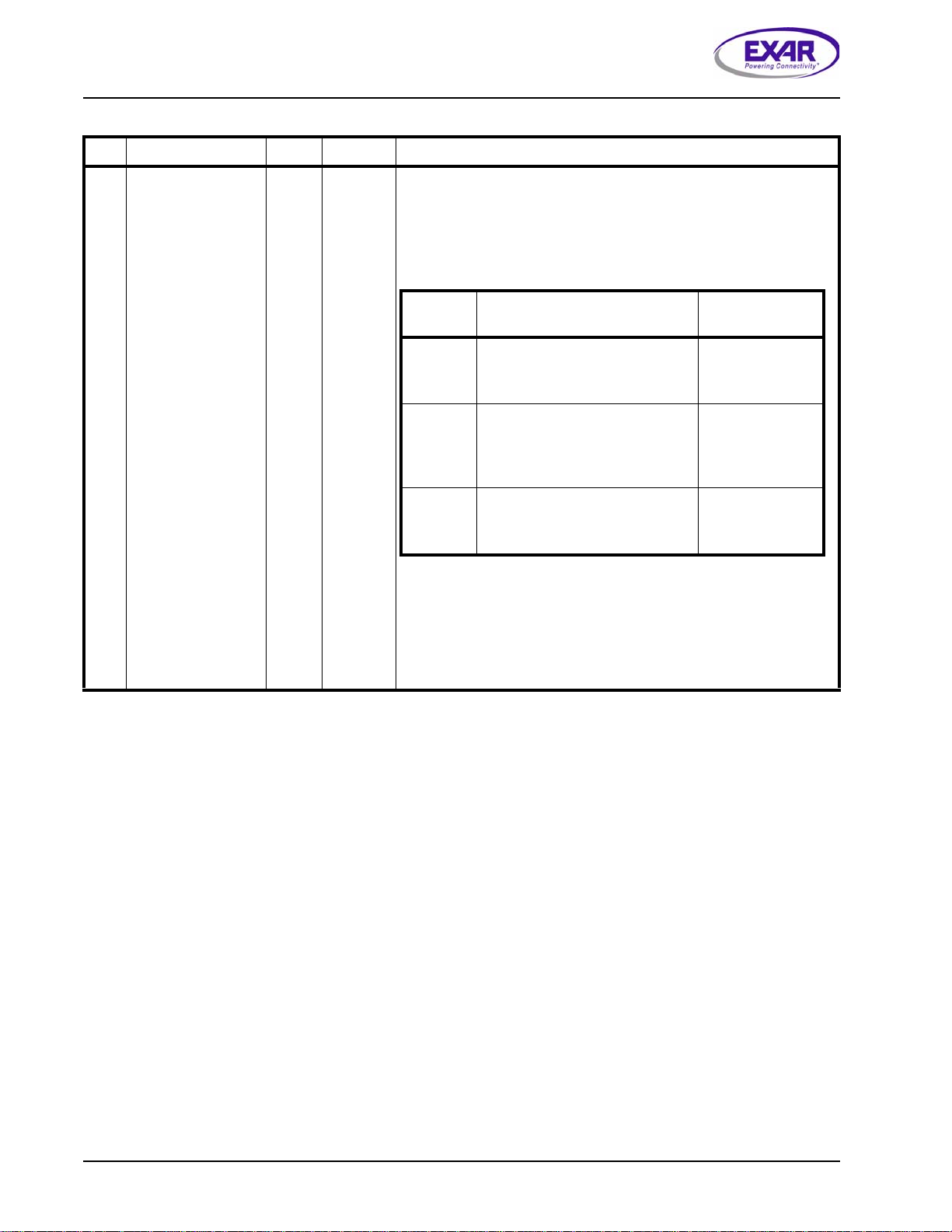
TABLE 2: CLOCK SELECT REGISTER(CSR) HEX ADDRESS: 0XN100
BIT FUNCTION TYPE DEFAULT DESCRIPTION-OPERATION
7LCV Insert R/W 0 Line Code Violation Insertion
This bit is used to force a Line Code Violation (LCV) on the transmit
output of TTIP/TRING.
A “0” to “1” transition on this bit will cause a single LCV to be inserted
on the transmit output of TTIP/TRING.
6Set T1 Mode R/W 0 T1 Mode select
This bit is used to program the individual channel to operate in either
T1 or E1 mode.
0 = Configures the selected channel to operate in E1 mode.
1 = Configures the selected channel to operate in T1 mode.
5 Sync All Transmit-
ters to 8kHz R/W 0 Sync All Transmit Framers to 8kHz
This bit permits the user to configure the Transmit T1 Framer block to
synchronize its “transmit output” frame alignment with the 8kHz signal
that is derived from the MCLK PLL, as described below.
0 - Disables the “Sync all Transmit Framers to 8kHz” feature.
1 - Enables the “Sync all Transmit Framers to 8kHz” feature.
NOTE: This bit is only active if the MCLK PLL is used as the “Timing
Source” for the Transmit T1 Framer” blocks. CSS[1:0] of this
register allows users to select the transmit source of the
framer.
4Clock Loss Detect R/W 1 Clock Loss Detect Enable/Disable Select
This bit enables a clock loss protection feature for the Framer when-
ever the recovered line clock is used as the timing source for the trans-
mit section. If the LIU loses clock recovery, the Clock Distribution Block
will detect this occurrence and automatically begin to use the internal
clock derived from MCLK PLL as the Transmit source, until the LIU is
able to regain clock recovery.
0 = Disables the clock loss protection feature.
1 = Enables the clock loss protection feature.
NOTE: This bit needs to be enabled in order to detect the clock closs
detection interrupt status (address: 0xNB00, bit 5)
3:2 Reserved R/W 00 Reserved
XRT86VX38
12
8-CHANNEL T1/E1/J1 FRAMER/LIU COMBO - T1 REGISTER DESCRIPTION REV. 1.0.3
1:0 CSS[1:0] R/W 01 Clock Source Select
These bits select the timing source for the Transmit T1 Framer block.
These bits can also determine the direction of TxSERCLK, TxSYNC,
and TxMSYNC in base rate operation mode (1.544MHz Clock mode).
In Base Rate (1.544MHz Clock Mode):
TABLE 2: CLOCK SELECT REGISTER(CSR) HEX ADDRESS: 0XN100
BIT FUNCTION TYPE DEFAULT DESCRIPTION-OPERATION
NOTE: TxSYNC/TxMSYNC can be programmed as input or output
depending on the setting of SYNC INV bit in Register Address
0xN109, bit 4. Please see Register Description for the
Synchronization Mux Register (SMR - 0xN109) Table 10.
NOTES:In High-Speed or multiplexed modes, TxSERCLK, TxSYNC,
and TxMSYNC are all configured as INPUTS only.
CSS[1:0] TRANSMIT SOURCE FOR THE
TRANSMIT T1 FRAMER BLOCK DIRECTION OF
TXSERCLK
00/11 Loop Timing Mode
The recovered line clock is cho-
sen as the timing source.
Output
01 External Timing Mode
The Transmit Serial Input Clock
from the TxSERCLK_n input pin is
chosen as the timing source.
Input
10 Internal Timing Mode
The MCLK PLL is chosen as the
timing source.
Output

XRT86VX38
13
REV. 1.0.3 8-CHANNEL T1/E1/J1 FRAMER/LIU COMBO - T1 REGISTER DESCRIPTION
TABLE 3: LINE INTERFACE CONTROL REGISTER (LICR) HEX ADDRESS: 0XN101
BIT FUNCTION TYPE DEFAULT DESCRIPTION-OPERATION
7FORCE_LOS R/W 0 Force Transmit LOS (To the Line Side)
This bit permits the user to configure the transmit direction circuitry
(within the channel) to transmit the LOS pattern to the remote terminal
equipment, as described below.
0 - Configures the transmit direction circuitry to transmit “normal” traffic.
1 - Configures the transmit direction circuitry to transmit the LOS
Pattern.
6Reserved R/W 0 Single Rail Mode
This bit can only be set if the LIU Block is also set to single rail mode.
See Register 0xNFE0, bit 7.
0 - Dual Rail
1 - Single Rail
5:4 LB[1:0] R/W 00 Framer Loopback Selection
These bits are used to select any of the following loop-back modes for
the framer section. For LIU loopback modes, see the LIU configuration
registers.
3:2 Reserved R/W 0 Reserved
LB[1:0] TYPES OFLOOPBACK SELECTED
00 Normal Mode (No LoopBack)
01 Framer Local LoopBack:
When framer local loopback is enabled, the transmit
PCM input data is looped back to the receive PCM out-
put data. The receive input data at RTIP/RRING is
ignored while an All Ones Signal is transmitted out to
the line interface.
10 Framer Far-End (Remote) Line LoopBack:
When framer remote loopback is enabled, the digital
data enters the framer interface, however does not
enter the framing blocks. The receive digital data from
the LIU is allowed to pass through the LIU Decoder/
Encoder circuitry before returning to the line interface.
11 Framer Payload LoopBack:
When framer payload loopback is enabled, the raw
data within the receive time slots are looped back to the
transmit framer block where the data is re-framed
according to the transmit timing.

XRT86VX38
14
8-CHANNEL T1/E1/J1 FRAMER/LIU COMBO - T1 REGISTER DESCRIPTION REV. 1.0.3
1Encode B8ZS R/W 0 Encode AMI or B8ZS/HDB3 Line Code Select
This bit enables or disables the B8ZS/HDB3 encoder on the transmit
path.
0 = Enables the B8ZS encoder.
1 = Disables the B8ZS encoder.
NOTE: When B8ZS encoder is disabled, AMI line code is used.
0Decode AMI/B8ZS R/W 0 Decode AMI or B8ZS/HDB3 Line Code Select
This bit enables or disables the B8ZS/HDB3 decoder on the receive
path.
0 = Enables the B8ZS decoder.
1 = Disables the B8ZS decoder.
NOTE: When B8ZS decoder is disabled, AMI line code is received.
TABLE 3: LINE INTERFACE CONTROL REGISTER (LICR) HEX ADDRESS: 0XN101
BIT FUNCTION TYPE DEFAULT DESCRIPTION-OPERATION

XRT86VX38
15
REV. 1.0.3 8-CHANNEL T1/E1/J1 FRAMER/LIU COMBO - T1 REGISTER DESCRIPTION
TABLE 4: GENERAL PURPOSE INPUT/OUTPUT 0 CONTROL REGISTER(GPIOCR0) HEX ADDRESS: 0X0102
BIT FUNCTION TYPE DEFAULT DESCRIPTION-OPERATION
7-4 GPIO0_3DIR
GPIO0_2DIR
GPIO0_1DIR
GPIO0_0DIR
R/W 1111 GPIO0_3/GPIO0_2/GPIO0_1/GPIO0_0 Direction
These bits permit the user to define the General Purpose I/O Pins,
GPIO0_3/GPIO0_2/GPIO0_1/GPIO0_0 as either Input pins or Output
pins, as described below.
0 – Configures GPIO0_3/GPIO0_2/GPIO0_1/GPIO0_0 to function as
input pins.
1 – Configures GPIO0_3/GPIO0_2/GPIO0_1/GPIO0_0 to function as
output pins.
1. If GPIO0_3/GPIO0_2/GPIO0_1/GPIO0_0 are configured to
function as input pins, then the user can monitor the state of
these input pins by reading out the state of Bit 3-0 (GPIO0_3/
GPIO0_2/GPIO0_1/GPIO0_0) within this register.
2. If GPIO0_3/GPIO0_2/GPIO0_1/GPIO0_0 are configured to
function as output pins, then the user can control the state of
these output pins by writing the appropriate value into Bit 3-0
(GPIO0_3/GPIO0_2/GPIO0_1/GPIO0_0) within this register.
3-0 GPIO0_3
GPIO0_2
GPIO0_1
GPIO0_0
R/W 0000 GPIO0_3/GPIO0_2/GPIO0_1/GPIO0_0 Control
The exact function of this bit depends upon whether General Purpose I/
O Pins, GPIO0_3/GPIO0_2/GPIO0_1/GPIO0_0 have been configured
to function as input or output pins, as described below.
If GPIO0_3/GPIO0_2/GPIO0_1/GPIO0_0 are configured to function
as input pins:
If GPIO0_3/GPIO0_2/GPIO0_1/GPIO0_0 are configured to function as
input pins, then the user can monitor the state of the corresponding
input pin by reading out the state of these bits.
NOTE: If GPIO0_3/GPIO0_2/GPIO0_1/GPIO0_0 are configured to
function as input pins, then writing to this particular register will
have no effect on the state of this pin.
If GPIO0_3/GPIO0_2/GPIO0_1/GPIO0_0 are configured to function
as output pins:
If GPIO0_3/GPIO0_2/GPIO0_1/GPIO0_0 are configured to function as
output pins, then the user can control the state of the corresponding
output pin by writing the appropriate value to these bits.
NOTE: GPIO0_3/GPIO0_2/GPIO0_1/GPIO0_0 can be configured to
function as input or output pins, by writing the appropriate
value to Bit 7-4 (GPIO0_3DIR/GPIO0_2DIR/GPIO0_1DIR/
GPIO0_0DIR) within this register.

XRT86VX38
16
8-CHANNEL T1/E1/J1 FRAMER/LIU COMBO - T1 REGISTER DESCRIPTION REV. 1.0.3
TABLE 5: GENERAL PURPOSE INPUT/OUTPUT 1 CONTROL REGISTER(GPIOCR1) HEX ADDRESS: 0X4102
BIT FUNCTION TYPE DEFAULT DESCRIPTION-OPERATION
7-4 GPIO1_3DIR
GPIO1_2DIR
GPIO1_1DIR
GPIO1_0DIR
R/W 0000 GPIO1_3/GPIO1_2/GPIO1_1/GPIO1_0 Direction
These bits permit the user to define the General Purpose I/O Pins,
GPIO1_3/GPIO1_2/GPIO1_1/GPIO1_0 as either Input pins or Output
pins, as described below.
0 – Configures GPIO1_3/GPIO1_2/GPIO1_1/GPIO1_0 to function as
input pins.
1 – Configures GPIO1_3/GPIO1_2/GPIO1_1/GPIO1_0 to function as
output pins.
1. If GPIO1_3/GPIO1_2/GPIO1_1/GPIO1_0 are configured to
function as input pins, then the user can monitor the state of
these input pins by reading out the state of Bit 3-0 (GPIO1_3/
GPIO1_2/GPIO1_1/GPIO1_0) within this register.
2. If GPIO1_3/GPIO1_2/GPIO1_1/GPIO1_0 are configured to
function as output pins, then the user can control the state of
these output pins by writing the appropriate value into Bit 3-0
(GPIO1_3/GPIO1_2/GPIO1_1/GPIO1_0) within this register.
3-0 GPIO1_3
GPIO1_2
GPIO1_1
GPIO1_0
R/W 0000 GPIO1_3/GPIO1_2/GPIO1_1/GPIO1_0 Control
The exact function of this bit depends upon whether General Purpose I/
O Pins, GPIO1_3/GPIO1_2/GPIO1_1/GPIO1_0 have been configured
to function as input or output pins, as described below.
If GPIO1_3/GPIO1_2/GPIO1_1/GPIO1_0 are configured to function
as input pins:
If GPIO1_3/GPIO1_2/GPIO1_1/GPIO1_0 are configured to function as
input pins, then the user can monitor the state of the corresponding
input pin by reading out the state of these bits.
NOTE: If GPIO1_3/GPIO1_2/GPIO1_1/GPIO1_0 are configured to
function as input pins, then writing to this particular register will
have no effect on the state of this pin.
If GPIO1_3/GPIO1_2/GPIO1_1/GPIO1_0 are configured to function
as output pins:
If GPIO1_3/GPIO1_2/GPIO1_1/GPIO1_0 are configured to function as
output pins, then the user can control the state of the corresponding
output pin by writing the appropriate value to these bits.
NOTE: GPIO1_3/GPIO1_2/GPIO1_1/GPIO1_0 can be configured to
function as input or output pins, by writing the appropriate
value to Bit 7-4 (GPIO1_3DIR/GPIO1_2DIR/GPIO1_1DIR/
GPIO1_0DIR) within this register.
Table of contents
Other Exar Amplifier manuals


