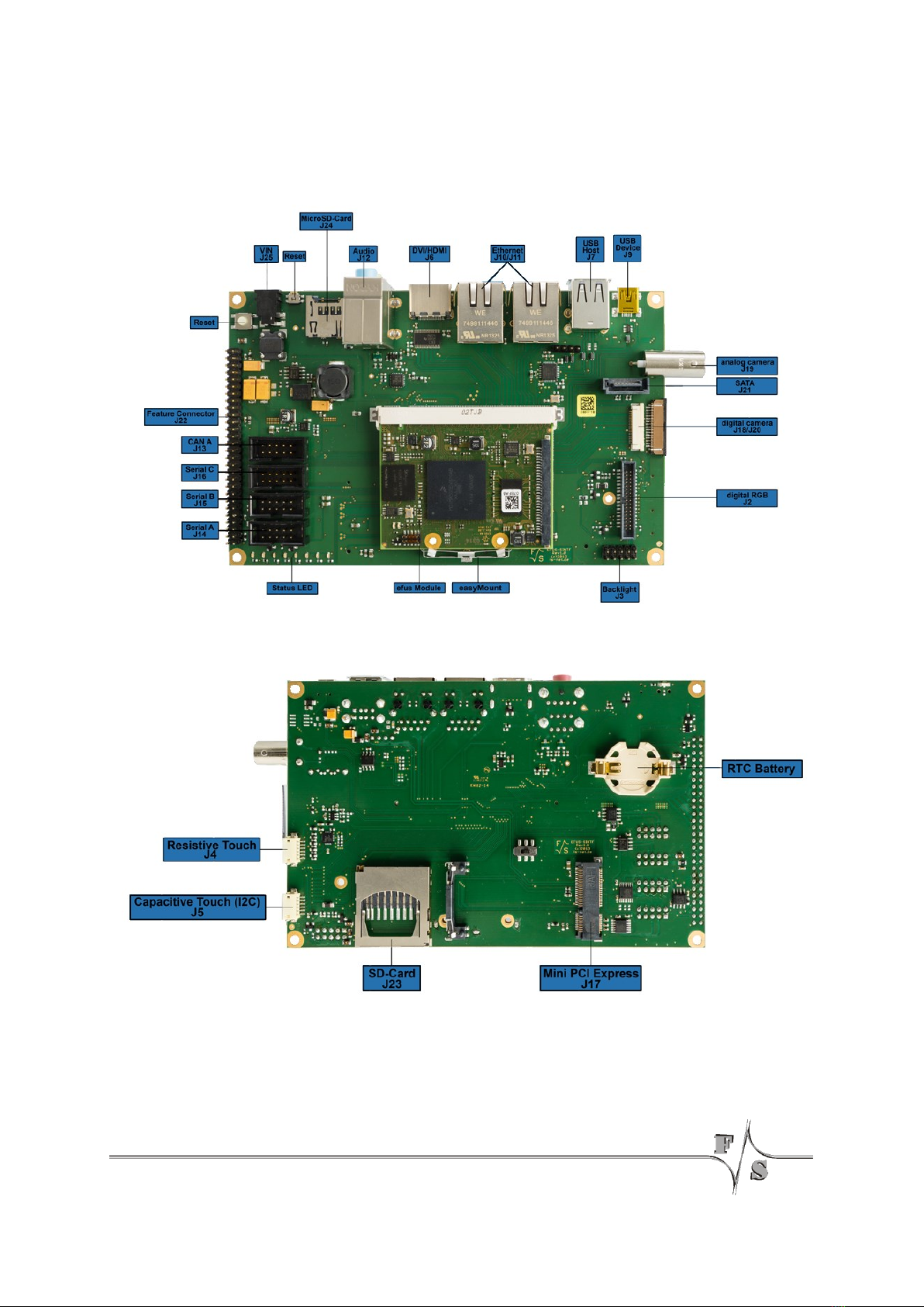
F&S efus-SINTF Operator's manual

Hardware documentation
for efus Startinterface
Version 1.0
(2014-03-10)
efus-
SINTF

About This Document
This document describes how to use the efus Startinterface board with mechanical and elec-
trical information. The latest version of this document can be found at:
http://www.fs-net.de.
History
Date
V
Platform
A,M,R
Chapter
Description
Au
21.02.14
0.1
All
A
-
Build the document
MW
V Version
A,M,R Added, Modified, Removed
Au Author

3
Table of Contents
About This Document 2
History 2
Table of Contents 3
1Introduction 5
2Mechanical dimension 6
2.1 Baseboard 7
2.2 Modules 7
3Connector layout 8
4Interface and signal description 9
4.1 J1 efus MXM-connector 9
4.2 J12 Sound 18
4.3 J7 / J8 USB host 19
4.4 J9 USB client 20
4.5 J13 CAN 21
4.6 J2 Digital RGB 22
4.6.1 J3 Display Power 24
4.7 J23 SD Card Interface 25
4.8 J24 MicroSD Card Interface 26
4.9 J6 DVI/HDMI 27
4.10 J22 F&S Feature-Connector 28
4.11 J10 / J11 Ethernet 30
4.12 J21 SATA 31
4.13 COM ports 32
4.13.1 J14 COM A 32
4.13.2 J15 COM B 32
4.13.3 J16 COM C 33
4.13.4 COM D 33
4.14 J25 / J26 Power 34
5Electrical characteristic 35
6Appendix 36
List of Figures 36
Important Notice 37
Warranty Terms 38

4

5
1 Introduction
The efus start interface is a base board for the efus family. It can be used with efusA9 or oth-
er boards of the efus family. For connecting it to a display, it has either DVI/HDMI, or the F&S
display connector for digital RGB, to be able to connect the same adapter like other F&S
boards.
For designing your own base board you can use our example Layout created with CadSoft
EAGLE® which you can get on our homepage http://www.fs-net.de.

6
2 Mechanical dimension
Figure 1: mechanical dimension

7
2.1 Baseboard
PCB size: 160mm x 100mm
PCB thickness: 1.6 ± 0.1mm
High of parts on the top side: 38mm
High of parts on the bottom side: 7.8mm
Weight: TBD
2.2 Modules
Size: 62.11mm x 47mm
PCB thickness: 1.2 ± 0.1mm
Height of the parts on the top side: TBD
Weight: TBD

8
3 Connector layout
Figure 3: Connector Layout Bottom
Figure 2: Connector Layout Top

9
4 Interface and signal description
4.1 J1 efus MXM-connector
The efus module is plugged on this connector.
The connector is a Foxconn 0.5mm MXMII connector part-no AS0B326-S78N-7F for 5mm
stacking height.
The efus module is fixed on the connector with the F&S EASYMOUNT technique.
See efus documentation for more information.
J1
Pin
Use on base board
Remarks
Connector
1
+5V Power In
2
+5V Power In
3
+5V Power In
4
+5V Power In
5
+5V Power In
6
+5V Power In
7
GND
8
GND
9
VBAT In
RTC battery input
J22/Battery
10
V33-Enable
EN for baseboard switcher.
3.3V VOUT with limited current.
Please refer module datasheet.
11
ACOK
J22
12
!RESET_IN
Drive with OC/OD, 3.3V PU on mod-
ule
J22
13
IOOUT_ADC_IN
J22
14
!RESET_OUT
Low active reset for baseboard logic
J22
15
RXD_C_TTL
Converted to RS485
J16
16
SD_A_WP
J24
17
TXD_C_TTL
Converted to RS485
J16

10
J1
Pin
Use on base board
Remarks
Connector
18
SD_A_CD
J24
19
RTS_C_TTL
Converted to RS485
J16
20
SD_A_DAT2
J24
21
CTS_C_TTL
22
SD_A_DAT3
J24
23
PWM_B
J22
24
SD_A_CMD
J24
25
PWM_A
J22
26
SD_A_VCC
J24
27
GND
28
SD_A_CLK
J24
29
CAN_A_TX
J13
30
GND
31
CAN_A_RX
J13
32
SD_A_DAT0
J24
33
GND
34
SD_A_DAT1
J24
35
CAN_B_TX
J22
36
RESERVED1
J22
37
CAN_B_RX
J22
38
RESERVED2
J22
39
GND
40
RESERVED3
J22
41
MPCIE_CTX_P
J17
42
RESERVED4
J22
43
MPCIE_CTX_N
J17
44
RESERVED5
J22

11
J1
Pin
Use on base board
Remarks
Connector
45
GND
46
GND
47
MPCIE_CRX_P
J17
48
EXT_PROG
J22
49
MPCIE_CRX_N
J17
50
SPI_B_MISO
J22
51
GND
52
SPI_B_MOSI
J22
53
MPCIE_CLK_P
J17
54
SPI_B_SPCK
J22
55
MPCIE_CLK_N
J17
56
SPI_B_CS1
J22
57
GND
58
SPI_B_CS2
J22
59
MPCIE_PERST
J17
60
SPI_B_IRQ1
J22
61
MPCIE_WAKE
J17
62
SPI_B_IRQ2
J22
63
GND
64
GND
65
SD_B_DAT2
J23
66
SPI_A_MISO
J22
67
SD_B_DAT3
J23
68
SPI_A_MOSI
J22
69
SD_B_CMD
J23
70
SPI_A_SPCK
J22
71
SD_B_VCC
J23

12
J1
Pin
Use on base board
Remarks
Connector
72
SPI_A_CS1
J22
73
SD_B_CLK
J23
74
SPI_A_CS2
J22
75
GND
76
SPI_A_IRQ1
J22
77
SD_B_DAT0
J23
78
SPI_A_IRQ2
J22
79
SD_B_DAT1
J23
80
GND
81
SD_B_WP
J23
82
I2C_B_DAT
PU on module
J22
83
SD_B_CD
J23
84
I2C_B_CLK
PU on module
J22
85
GND
86
I2C_B_IRQ
PU on module
J22
87
BL_CTRL
PWM Backlight dimming
J3
88
I2C_B_RST
J22
89
VCFL_ON
Backlight on
J3
90
GND
91
GND
92
RXD_A_TTL
Debug; Converted to RS232
J14
93
LCD_CLK
J2
94
TXD_A_TTL
Debug; Converted to RS232
J14
95
GND
96
RXD_D_TTL
J22
97
LCD_HSYNC
J2
98
TXD_D_TTL
J22

13
J1
Pin
Use on base board
Remarks
Connector
99
LCD_VSYNC
J2
100
GND
101
GND
102
RXD_B_TTL
Converted to RS232
J15
103
LCD_R0
J2
104
TXD_B_TTL
Converted to RS232
J15
105
LCD_R1
J2
106
RTS_B_TTL
Converted to RS232
J15
107
LCD_R2
J2
108
CTS_B_TTL
Converted to RS232
J15
109
LCD_R3
J2
110
GND
111
LCD_R4
J2
112
I2S_MCLK
J12
113
LCD_R5
J2
114
GND
115
GND
116
I2S_LRCLK
J12
117
LCD_G0
J2
118
GND
119
LCD_G1
J2
120
I2S_SCLK
J12
121
LCD_G2
J2
122
GND
123
LCD_G3
J2
124
I2S_DOUT
J12
125
LCD_G4
J2

14
J1
Pin
Use on base board
Remarks
Connector
126
I2S_DIN
J12
127
LCD_G5
J2
128
GND
129
GND
130
I2C_C_DAT
131
LCD_B0
J2
132
I2C_C_CLK
133
LCD_B1
J2
134
DVI_DDC_VOUT
3.3V output for ESD protection
J6
135
LCD_B2
J2
136
GND
137
LCD_B3
J2
138
DVI_DATA2_P
J6
139
LCD_B4
J2
140
DVI_DATA2_N
J6
141
LCD_B5
J2
142
DVI_DATA1_P
J6
143
GND
144
DVI_DATA1_N
J6
145
LCD_DE
J2
146
DVI_DATA0_P
J6
147
GND
148
DVI_DATA0_N
J6
149
VLCD_ON
J3
150
DVI_CLK_P
J6
151
I2C_A_DAT
J2/J5
152
DVI_CLK_N
J6

15
J1
Pin
Use on base board
Remarks
Connector
153
I2C_A_IRQ
J2/J5
154
GND
155
I2C_A_CLK
J2/J5
156
DVI_DDCCEC
J6
157
I2C_A_RST
J5
158
DVI_HPD
J6
159
GND
160
GND
161
CAM_YDATA9/D0_N
J18/J20
162
ETH_B_D4_N
J10
163
CAM_YDATA8/D0_P
J18/J20
164
ETH_B_D4_P
J10
165
CAM_YDATA2/D1_N
J18/J20
166
ETH_B_LED_LINK
J10
167
CAM_YDATA1/D1_P
J18/J20
168
ETH_B_D3_N
J10
169
CAM_YDATA3/D2_N
J18/J20
170
ETH_B_D3_P
J10
171
CAM_YDATA0/D2_P
J18/J20
172
GND
173
CAM_YDATA4/D3_N
J18/J20
174
ETH_B_D2_N
J10
175
CAM_PCLK/D3_P
J18/J20
176
ETH_B_D2_P
J10
177
CAM_YDATA5/CLK_N
J18/J20
178
ETH_B_LED_ACT
J10

16
J1
Pin
Use on base board
Remarks
Connector
179
CAM_YDATA6/CLK_P
J18/J20
180
ETH_B_D1_N
J10
181
GND
182
ETH_B_D1_P
J10
183
CAM_MCLK
J18/J20
184
GND
185
GND
186
ETH_CTREF
J10/J11
187
CAM_YDATA7
J18
188
ETH_A_D4_N
J11
189
CAM_VCAM
J18
190
ETH_A_D4_P
J11
191
CAM_HREF
J18
192
ETH_A_LED_LINK
J11
193
CAM_PWDN
J18/J20
194
ETH_A_D3_N
J11
195
CAM_VSYNC
J18
196
ETH_A_D3_P
J11
197
I2C_C_CAMRST
J18
198
ETH_A_VLEDOUT
VOUT for LAN LEDs
J11
199
GND
200
ETH_A_D2_N
J11
201
SATA_RX_P
J21
202
ETH_A_D2_P
J11
203
SATA_RX_N
J21
204
ETH_A_LED_ACT
J11

17
J1
Pin
Use on base board
Remarks
Connector
205
SATA_TX_N
J21
206
ETH_A_D1_N
J11
207
SATA_TX_P
J21
208
ETH_A_D1_P
J11
209
GND
210
GND
211
CAM_A_IN
Analog Camera IN
J19
212
USB_A_PWRON
J7/J8/J17
213
CAM_A_GND
Analog Camera Ground
J19
214
USB_A_N
J7/J8/J17
215
GND
216
USB_A_P
J7/J8/J17
217
USB_DEV_VBUS
J9
218
GND
219
USB_DEV_PWR_ON
J9
220
USB_A_SSRX_N
/
221
USB_DEV_OC
J9
222
USB_A_SSRX_P
/
223
USB_DEV_ID
J9
224
GND
225
USB_DEV_N
J9
226
USB_A_SSTX_N
/
227
USB_DEV_P
J9
228
USB_A_SSTX_P
/
229
GND
230
GND

18
4.2 J12 Sound
The sound connector does provide Stereo Line In, Stereo Line Out and Microphone In.
Figure 4: Audio connection

19
4.3 J7 / J8 USB host
All USB ports follow the USB 2.0 specification.
With a Hub, the single USB-Port of the efus module is expanded to four USB Ports (A - D).
Port A & B are connected to the USB Host front connector. USB Port C is connected to a 4
pin header. USB Port D is connected to the mPCIE connector.
The 90 Ohm differential pair of USB signals doesn’t need any termination. For external ports,
EMV protection is required nearby the USB connector.
The usb.org webpage provides “High Speed USB Platform Design Guidelines“ with highly
recommended information for a proper working USB design.
If a USB port is not used, please leave it open.
Figure 5: USB Host with USB Hub

20
4.4 J9 USB client
It’s a standard USB mini connector to use the board as USB device.
Figure 6: USB device
Table of contents