Forenex MBE71 User manual

`
-1-
MBE71
User
Manual
MBE71
Motherboard
User Manual
(Preliminary)
SBC
with Dual Cortex-A72 @2.0Ghz
+ Quad Cortex-A53 @ 1.5Ghz Core
Version: V3.0
Document No: doc-mbe7118w40v30
PCB Bare Board: PB71m68v11
*The content of this document is subject to be change without notice

`
-2-
MBE71
User
Manual
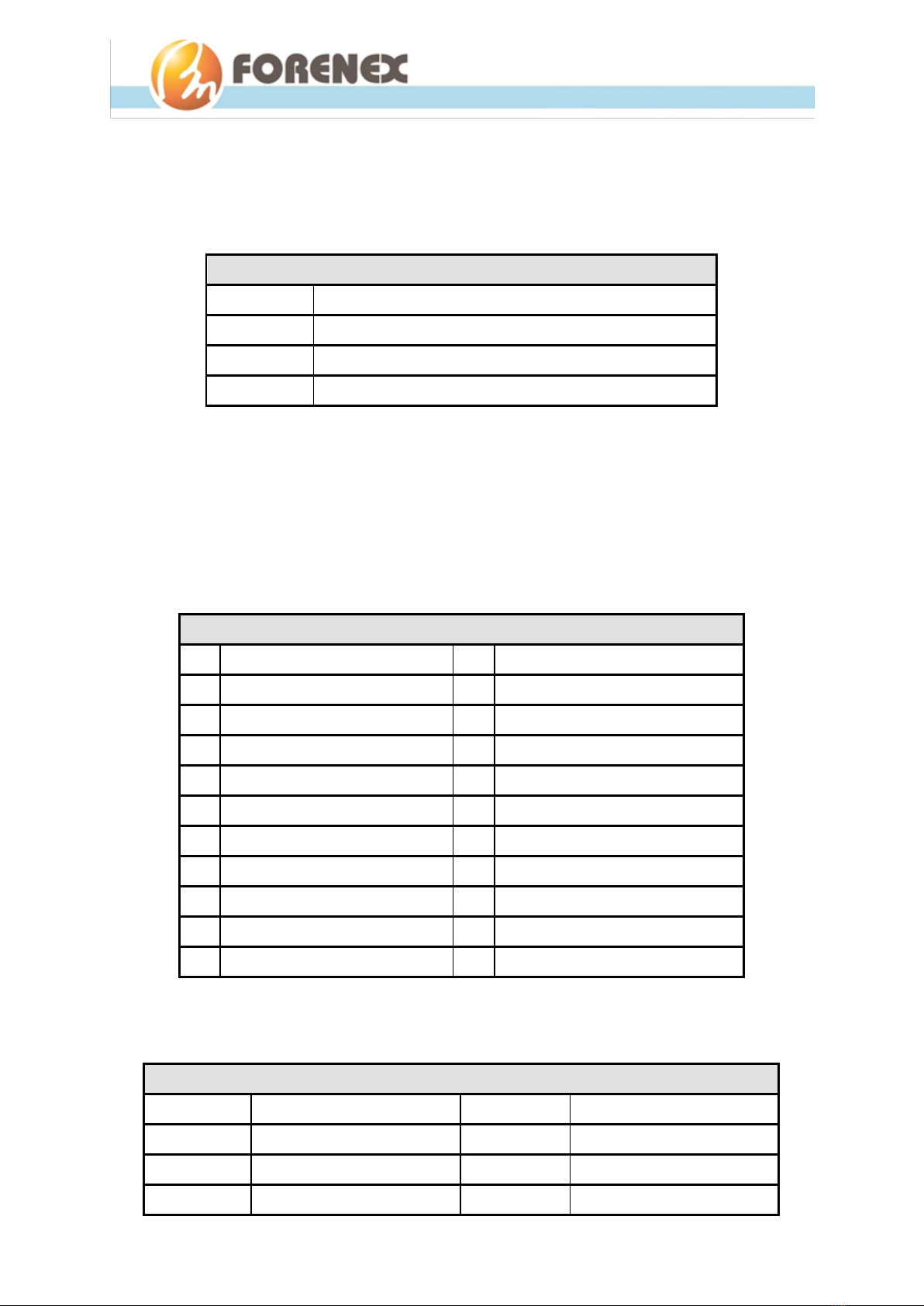
Packing List
1 x MBE71 Motherboard.
Ordering Information
Part Number: MBE71-abcxyMN
HDMI 2.0, eDP1.3 (2xlane), GigE, 5G-Wifi with mPCIE Socket, OTG-USB 3.0 (Type-
A), USB2.0 (Type-A), Micro-SD Socket, Grove GPIOs, Reset CONN, Optic Fiber CONN, 4-
wire UART Port, IR Port, Debug Port, Audio, USB-Hub, DC-Jack.
• abc : The type of RK3399 Processor
R39: Dual Core-A72 @2.0Ghz,+ Quad Core-A53 @ 1.5Ghz, (0 ~ 85°C)
K39: Dual Core-A72 @2.0Ghz,+ Quad Core-A53 @ 1.5Ghz, ( -20°~ 105°C)
• x: The size code of DDR3 Memory on board
1 1GB of DDR3
2 2GB of DDR3
• y: The size code of eMMC on board
4 4GB
8 8GB
F 16GB
• MN : The Function code
SS Standards
S1 Add Wi-Fi module
PS SS + 802.3at (PoE+)
P1 S1 + 802.3at (PoE+)
Optional Accessories
FEP21-B4356C AP12356,11 a/b/g/n/ac (2T2R)+BT(V4.1 LE), Wi-Fi module
FR-e2L eDP to Dual LVDS Converter Board
FR-U2R2 USB to Dual full RS232/RS422/485 Convert Board
FR-WW01 USB to LTE 4G module Carrier Board

`
-3-
MBE71
User
Manual
Revision histories
Rev. No.
Date
Substantial Changes
1.0
2021/01
First issue.

`
-4-
MBE71
User
Manual
Table of Contents
1. General Information ........................................................................................................... 6
1-1. Features ................................................................................................................................. 6
1-2. Function Block Diagram ......................................................................................................... 8
1-3. Board Dimension.................................................................................................................... 9
1-4. I/O Connector Summary ........................................................................................................ 9
1-5. I/O Connector Placement .................................................................................................... 10
2. Peripherals Port Description............................................................................................. 11
2-1. Power Jack (J4)(W4)............................................................................................................. 11
2-2. Power Switch, Header (H15)................................................................................................ 11
2-3. RTC Battery Backup Connector (W1)................................................................................... 11
2-4. IR Receiver Connector (IR1) ................................................................................................. 12
2-5. Power LED Connector (W7) ................................................................................................. 12
2-6. Image File Update Jumper (JP1) .......................................................................................... 12
2-7. USB 3.0 Type-A Port (J2) ...................................................................................................... 13
2-8. USB 2.0 Type-A Port (J3) ...................................................................................................... 13
2-9. Gigabit Ethernet Port w/PoE+ (J6)....................................................................................... 14
2-10. PoE+ Power Extract Connector (W12)................................................................................. 14
2-11. Micro SD/SDHC Card Slot (J1) .............................................................................................. 14
2-13. eDP Interface (ZIF2) ............................................................................................................. 15
2-14. LCD Panel Power Selection (H2) .......................................................................................... 16
2-15. LCD Backlight Control Connector (W2)................................................................................ 16
2-16. PCAP Touch Interface (W3).................................................................................................. 16
2-17. HDMI® 2.0 Port (J5).............................................................................................................. 17
2-18. Reset, wifi LEDs, Buzzer Combo Connector (W19) .............................................................. 17
2-19. RS232 Debug Connector (W20) ........................................................................................... 18
2-20. Grove-I2C,SPI,ADC,GPIOs Connector (W15)........................................................................ 18

`
-5-
MBE71
User
Manual
2-22. USB host2.0, MEMS signals Combo Connector (W10) ........................................................ 19
2-23. HUB Extended Ports (W8, W9, W18)................................................................................... 19
2-24. Audio Codec Interface (H10)................................................................................................ 20
2-25. mini-PCIe Slot(J9) ................................................................................................................. 21
2-26. MIPI-CSI Interface (W13) (Optional) ,Under development.................................................. 22
3. Software Programming Guide .......................................................................................... 23
3-1. Android Programming Guide............................................................................................... 23
3-1-1. ADB installation...............................................................................................23
3-1-2. To install APK software over the ADB function of PC : ..........................................25
3-1-3. GPIO installation..............................................................................................25
3-2. Linux Programming Guide.................................................................................................... 26
3-2-1. GPIO installation..............................................................................................26

`
-6-
MBE71
User
Manual
1. General Information
The motherboard MBE71 Series integrated various useful peripheral circuit that provides
completed connectivity for a wide variety of industrial automation and transportation
applications. Besides, the high-performance media-processor also especially for
infotainment/entertainment, HMI applications.
The heart of the MBE71 is the Dual Cortex-A72 @2.0Ghz + Quad Cortex-A53 @ 1.5Ghz
processor, which provides a complete platform for project evaluation and solution feasibility
testing that decreases the time to market and lowers initial cost.
1-1. Features
Processor:
Dual Cortex-A72 @2.0Ghz + Quad Cortex-A53 @ 1.5Ghz (MBE70Kxx)
Dual Cortex-A72 @2.0Ghz + Quad Cortex-A53 @ 1.5Ghz (MBE70xx)
System Memory:
1GB up to 2GB DDR3-1066 SDRAM onboard
Storage:
4GB up to 16GB eMMC Flash memory
Graphics:
ARM Mail-T860MP4 (Embedded 3D GPU), AFBC supported
Supports OpenGL ES1.1/2.0/3.0/3.1, OpenVG1.1, OpenCL, DX11
Video Decoder:
-H.264/H.265, 10bit, up to 4Kx2K@60fps,
-VP9, 8bit, up to 4Kx2K@60fps,
-MPEG-4/MPEG-2/VP8 up to 1080p@60fps
Video Encoder:
-H.264/MVC/VP8 encoders by 1080p@30fps
Display Interfaces:
Supports eDP 1.3, 2 lane (2.7Gbps per lane) , Res. up to1920x1200p@60fps
, 4 lane (2.7Gbps per lane) , Res. up to2560x1600p@60fps
Supports HDMI® V2.0, Res. up to 4Kx2K @60fps, HDCP1.4 /2.2

`
-7-
MBE71
User
Manual
Audio:
Realtek ALC5640 low power stereo codec
Inside Stereo Class-D speaker amplifiers provide 1.5W per channel into 8Ω or 2W
per channel into 4Ω
LAN:
Realtek RTL8211E Gigabit Ethernet transceiver with RGMII support
Extension USB device:
MicroChip USB2514, USB 2.0 high speed 4-port hub controllers
External extension memory Slot:
Micro-SD 3.0 slot enable capacity up to 256GB
Various interfaces for expansion peripherals:
USB-HUB Port Wafer x 3
Optic Fiber Wafer x 1, 4-wire UART Wafer x 1
Grove (I2C, SPI, ADC, GPIOs) Wafer x 1
Optional MIPI-CSI/DSI interface x 1, MEMS Wafer x 1, IR receiver Wafer x 1
Dimension (W x D x H):
126.5mm x 90mm x 18.7mm (4.98” x 3.5” x 0.76”)
Operating Temperature (3G and Wi-Fi not included):
-20°C ~ 70°C (MBE70E-K39 series)
0°C ~ 70°C (MBE70C-R39 series)
Operating Humidity:
0% ~ 90% relative humidity (non-condensing)
Operating System:
Android 7.1 / 8
Debian 9
Note:
1. The Operating Temperature is a result of the test performed in experimental
chamber. It is highly suggested to execute a solid testing under actually application
environment.
2. More frequent and larger data access on eMMC memory makes the lifespan
shorter. Therefore, it is highly recommended to use a Micro SD card for large data
access.
`
-8-
MBE71
User
Manual
1-2. Function Block Diagram

`
-9-
MBE71
User
Manual
1-3. Board Dimension
Dimension: 126.5mm (W) x 90mm (L) x 18.7mm (H)
Contact Service salesman for detail “.DXF” file.
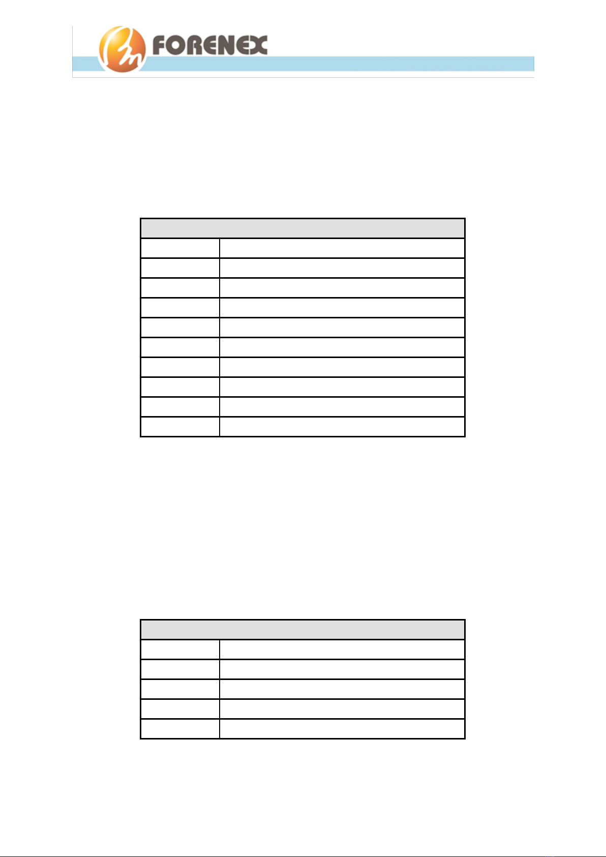
1-4. I/O Connector Summary
External I/O (On board side):
Power Jack (J4),(W4)
Micro SD Socket (J1)
USB 3.0 Type-A Port (J2)
USB 2.0 Type-A Port (J3)
HDMI® Port (J5)
Gigabit Ethernet Port w/ PoE+ (J6)
Internal I/O
Image File Update Jumper (JP1)
RTC Battery Backup CONN (W1)
Power Switch, Header (H15)
Power LED CONN (W7)
USB host2.0, MEMS signals Combo CONN (W10)
Grove-I2C,SPI,ADC,GPIOs Combo CONN (W15)
Optic Fiber Light-Bar CONN (W14)
eDP Interface (ZIF2)
LCD Panel Power Selection, Header (H2)
LCD Backlight Control CONN (W2)
PCAP Touch CONN (W3)
4-wire UART CONN (W17)
RS232 Debug CONN (W20)
Reset, Wi-Fi LED, Buzzer Combo CONN (W19)
PoE+ Power Extract CONN (W12)
HUB Extended Ports, CONNs (W8, W9, W18)
Audio Codec Interface, Header (H10)
Mini-PCIe Slot (J9) for AP12356, 802.11 a/b/g/n/ac (2T2R)+BT(V4.1 LE) module
------Provides below are optional items ------
IR Receiver Connector, Wafer (IR1)
MIPI-CSI/DSI Interface (W13)
`
-10-
MBE71
User
Manual
1-5. I/O Connector Placement
Component Side
Solder Side

`
-11-
MBE71
User
Manual
2. Peripherals Port Description
2-1. Power Jack (J4、W4)
Carries external power input.
If necessary, also provides extra DC/DC convert board with the wide range (9V to
36V) input voltage and a steady 12V output.
Pin Assignment(J4、W4):
2-2. Power Switch, Header (H15)
Shorts the Pin 1&2 of the H15, to power up MBE71 mainboard.
The Pin 3 & 4 of the H15 reserved.
2-3. RTC Battery Backup Connector (W1)
Connect to the non-rechargeable coin battery.
Pin Assignment:
Connector: (Power Barrel Jack6.3mm/ Tip2.0mm/ 90°)
Pin number(J4)
Pin number(W4)
Description
Sleeve
Pin1
GND
Tip
Pin2
DC12V
Connector: (Header 2x2 pin/ 2.0mm/ 180°)
Pin number
Status
Description
Pin 1-2
Open
Power off
Close
Power on
Pin 3-4
Leave Open
For factory use only
Connector: (wafer-2P/ 1.25mm/ 180°)
Pin number
Description
1
3.0V(+)
2
GND(-)
Open
Close
`
-12-
MBE71
User
Manual
2-4. IR Receiver Connector (IR1)
Connects an external IR-38.8Khz receiver module
Pin Assignment:
2-5. Power LED Connector (W7)
The green LED indicates the system’s power is plugged.
Pin Assignment:
2-6. Image File Update Jumper (JP1)
To open the JP1 before power-on that would make system to enter Image-File-
Update mode at power re-plug-in. After that, close the JP1 and beginning update
Image File from the USB port (J2).
Connector: (wafer-3P/ 1.25mm/ 180°)
Pin number
Description
1
IR Signal input(1k ohm of Series resistor inside)
2
GND
3
3.3V supply
Connector: (wafer-3P/ 1.25mm/ 180°)
Pin number
Description
1
Green Light
2
GND
3
Reserved for Red Light
JP1 Open
JP1 Close
`
-13-
MBE71
User
Manual
2-7. USB 3.0 Type-A Port (J2)
The dedicated USB port to in charge of updating the Image File while the MBE71
board being enter update mode. Refer to Section 2-6.
Under Linux OS environment, the J2 is regarded as an USB3.0 host. And gives
complete hot plug capability and complies with USB xHCI, Rev. 3.x (USB 3.1 Gen 1).
Under Android OS environment, the J2 can be set to host or device mode. The
detail refer to Section 3-1. Android Programming Guide.
Pin Assignment:
2-8. USB 2.0 Type-A Port (J3)
The MBE71 provides one USB 2.0 host port on board side that gives complete hot
plug capability and complies with USB UHCI, Rev. 2.0.
Pin Assignment:
Connector: (USB 3.0 Type-A )
Pin number
Description
Pin number
Description
1
VBUS
6
SSRX+
2
D-
7
GND
3
D+
8
SSTX-
4
GND
9
SSTX+
5
SSRX-
Connector: (USB Type A )
Pin number
Description
1
VBUS1(+5V)
2
USB1 Data -
3
USB1 Data +
4
USB1_GND

`
-14-
MBE71
User
Manual
2-9. Gigabit Ethernet Port w/PoE+ (J6)
The integrated 8-pin Gigabit Ethernet port is using an 8 Position 8 Contact (8P8C)
receptacle connector (commonly referred to as RJ-45).
Supports IEEE802.3 at compliant (type2) PD.
The Gigabit Ethernet port (RJ-45 port) has two individual LED
indicators located on the front side to show
Active LED is blinking in green color means that
activity of data flow IN or OUT of the device.
Link LED is in Red color means devices is operating in speeds 10/100Mbps.
Link LED is in Green color means devices is operating in speeds 1000Mbps.
2-10. PoE+ Power Extract Connector (W12)
There are two modes of PoE, A and B. Mode A delivers power on the data pairs of
Pin1,2&3,6 of Gigabit Ethernet Port (J6). Mode B delivers power on the Pin4,5&7,8
of Gigabit Ethernet Port (J6).
2-11. Micro SD/SDHC Card Slot (J1)
Micro SD/SDHC card slot enable SD card capacity up to 256GB.
Providing as an extra-storage device. Prevent more frequent and larger data access
on eMMC memory makes its lifespan shorter.
2-12. 4-wire UART Connector (W17)
Connector: ( wafer-4P/ 2.0mm/ 180°)
Pin number
Description
Pin number
Description
1
V+ (Mode A)
2
V- (Mode A)
3
V+ (Mode B)
4
V- (Mode B)
Connector: ( wafer-8P/ 1.0mm/ 180°)
Pin number
Description
Pin number
Description
1
DC3.3V/60mA-Out
2
GND
3
UART-3.3V-RTS
4
UART-3.3V-CTS
5
UART-3.3V-TX(SOUT)
6
UART-3.3V-RX(SIN)
Act
100M/Giga

`
-15-
MBE71
User
Manual
2-13. eDP Interface (ZIF2)
Supports eDP 1.3(2.7Gbps per lane). 4 Lane with connector A1253WR-S-40P is
defaulted in factory.
Supports 2 Lane, Res. up to1920x1200p@60fps with connector A1253WR-S-30P.
Supports 4 Lane, Res. up to2560x1600p@60fpswith connector A1253WR-S-40P.
Pin Assignment: (*The blue signs reserved for future use)
Connector: (TFP584-30P/40P, 0.5mm, 90
°
)
Pin number
Description
Pin number
Description
1
NC
21
BL_GND
2
GND
22
BL_EN_H
3
Lane1_N
23
BL_PWM_DIM
4
Lane1_P
24
NC/Lane2_N
5
GND
25
NC/Lane2_P
6
Lane0_N
26
BL_VLED_12V
7
Lane0_P
27
BL_VLED_12V
8
GND
28
BL_VLED_12V
9
AUX_P
29
BL_VLED_12V
10
AUX_N
30
NC/Lane3_N
11
GND
31
NC/TP_USB_DM
12
LCD_VDD
32
NC/TP_USB_DP
13
LCD_VDD
33
GND
14
LCD_VDD
34
NC/TP_PWR
15
GND
35
NC/TP_PWR
16
GND
36
NC/Lane3_P
17
HPD
37
NC/TP_SCL
18
BL_GND
38
NC/TP_SDA
19
BL_GND
39
NC/TP_INT
20
BL_GND
40
NC/TP_RST

`
-16-
MBE71
User
Manual
2-14. LCD Panel Power Selection (H2)
Provides 3.3V to LCD_VDD Provides 5V to LCD_VDD
2-15. LCD Backlight Control Connector (W2)
The voltage of BL_VDD is same as DC_IN, due to the power source of BL_VDD is
passed from DC-in Jack (J4) or (W4) directly.
Pin Assignment:
2-16. PCAP Touch Interface (W3)
USB interface is defaulted touch port in factory; it can change to I2C interface
before ordering.
Pin Assignment:
Connector: (Wafer-6p/ 1.25mm/ 90
°
)
Pin number
Description
1
BL_VDD(12V) (default)/ 5V (option)
2
BL_VDD(12V)
3
GND
4
GND
5
Backlight_EN (active high), logical high level(3.3V)
6
Backlight_PWM (300Hz), logical high level(3.3V)
Connector: ( Wafer-6p/ 1.25mm/ 90
°
)
Pin number
Description
1
GND
2
Power supply DC-5V
3
USB_DP (default)/ SCL (option), logical high level(3.3V)
4
USB_DM (default)/ SDA (option), logical high level(3.3V)
5
INT, logical high level (3.3V)
6
Reset, logical high level(3.3V)

`
-17-
MBE71
User
Manual
2-17. HDMI® 2.0 Port (J5)
The HDMI port uses an HDMI Type-A receptacle connector. It allows connecting the
digital video devices which utilize a high definition video signal without a HDCP.
Supports HDMI® V2.0, Res. up to 4Kx2K(30-bit/pixel) @60fps, HDCP1.4 /2.2
Pin Assignment:
2-18. Reset, wifi LEDs, Buzzer Combo Connector (W19)
Connector: (19-pin HDMI Type A Receptacle,4.45 mm×13.9 mm)
Pin
Description
Pin
Description
1
TMDA_Data2+
2
Data2_GND
3
TMDA_Data2-
4
TMDA_Data1+
5
Data1_GND
6
TMDA_Data1-
7
TMDA_Data0+
8
Data0_GND
9
TMDA_Data0-
10
TMDA_CLK+
11
CLK_GND
12
TMDA_CLK-
13
NC
14
NC
15
DDC-SCL, logical high level(5V)
16
DDC-SDA, logical high level(5V)
17
CEC GND
18
Power 5V supply
19
Hot Plug Detect
Connector: ( A1001WV-S-8P/ 1.0mm/ 180°)
Pin number
Description
Pin number
Description
1
DC3.3V/25mA-Out
2
GND
3
Wifi LED-Out, Low active
4
BT LED-Out, Low active
5
Reset-In, Low active
6
GND
7
Buzzer-
8
Buzzer+
`
-18-
MBE71
User
Manual
2-19. RS232 Debug Connector (W20)
The debug port supports TX/RX with RS232 level and only use for debug purpose.
Pin Assignment:
2-20. Grove-I2C,SPI,ADC,GPIOs Connector (W15)
Supports Non-isolated GPIOs: GPI x4, GPO x4
ADC (Analog to Digital Channel_0 & 1), the Max. Input Voltage =1.8V, Res. 10bit,
tCLK=75ns, conversion time= 13tCLK, setup time=0.5tCLK.
Pin Assignment:
2-21. Optic Fiber Light-Bar Connector (W14)
Connector: ( wafer-3P/ 1.25mm/ 180°)
Pin number
Description
1
Debug-RS232-RX(SIN)
2
Debug-RS232-TX(SOUT)
3
COM_GND
Connector: (A1001WV-S-2x10P/ 1.0mm/ 180°)
Pin
Description
Pin
Description
1
DIN0, logical high level(3.3V)
2
DOUT0, logical high level(3.3V)
3
DIN1, logical high level(3.3V)
4
DOUT1, logical high level(3.3V)
5
DIN2, logical high level(3.3V)
6
DOUT2, logical high level(3.3V)
7
DIN3, logical high level(3.3V)
8
DOUT3, logical high level(3.3V)
9
GND
10
3.3V
11
SPI-3.3V-TXD
12
3.3V
13
SPI-3.3V-RXD
14
I2C4-3.3V-SDA
15
SPI-3.3V-CS
16
I2C4-3.3V-SCL
17
SPI-3.3V-CLK
18
ADC1-IN-1.8V
19
GND
20
ADC0-IN-1.8V
Connector: ( A1001WV-S-6P/ 1.0mm/ 180°)
Pin number
Description
Pin number
Description
1
Red, Low active
2
Green, Low active
3
Blue, Low active
4
White, Low active
5
GND
6
5V/500mA
`
-19-
MBE71
User
Manual
2-22. USB host2.0, MEMS signals Combo Connector (W10)
The connector (W10) can be either used as an extra USB 2.0 individually.
Or use for a LTE 4G modem module application.
Or use for a USB-MEMS application.
Pin Assignment:
2-23. HUB Extended Ports (W8, W9, W18)
The Wafer (W8) is designed to extend one more USB port.
The Wafer (W18) is designed to extend second USB port.
The Wafer (W9) is designed to either extend third USB port or as USB-touch panel
interface.
The all of three extended USB ports give complete hot plug capability and complies
with USB UHCI, Rev. 2.0.
The Pin Assignment (W8),(W9)(W18):
Connector: ( Wafer 1x9/ 1.25mm/ 90°)
Pin number
Description
1
LIGHT_INT_L (3.3V), Low active
2
GPIO(3.3V) Reserved
3
COMP_INT_L(3.3V), Low active
4
GSENSOR_INT_L(3.3V), Low active
5
GYR_INT_L(3.3V), Low active
6
USB_GND
7*
USB Data +
8
USB Data -
9
VBUS(+5V)
Connector: ( Wafer 1x4/ 1.25mm/ 90°)
Pin number
Description
1
VBUS3(+5V)
2
USB3 Data -
3
USB3 Data +
4
USB3_GND
`
-20-
MBE71
User
Manual
2-24. Audio Codec Interface (H10)
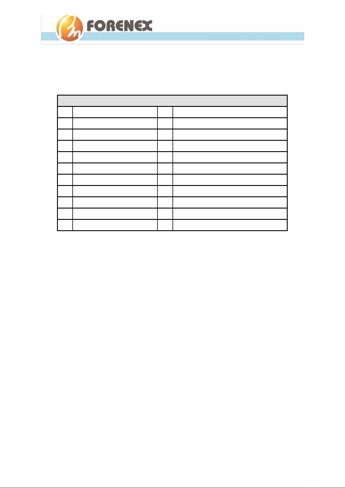
Supports speaker amplifiers 1.5W per channel into 8Ω or 2W per channel into 4Ω.
Pin Assignment:
Connector: (Header 2x10 pin/ 2.0mm/ 180°)
Pin
Description
Pin
Description
1
GND
2
HP_R
3
MIC_IN
4
HP_L
5
HP_GND
6
HP Plug-in detection, (3.3V)high active
7
SPK_R-
8
SPK_R+
9
SPK_L-
10
SPK_L+
11
GND
12
GND
13
Stereo_MIC_R /(LINE_IN_R)
14
Stereo_MIC_L /(LINE_IN_L)
15
LINE_OUT_L
16
LINE_OUT_R
17
Reserved for SPDIF_GND
18
GND
19
Reserved for SPDIF_VCC
20
Reserved for SPDIF_TX
This manual suits for next models
1
Table of contents


