ECS Electronics P4VXAD Rev.3.1 User manual

i
Preface
Copyright
This publication, including all photographs, illustrations and software, is protected un-
der international copyright laws, with all rights reserved. Neither this manual, nor any
of the material contained herein, may be reproduced without writtenconsent ofthe au-
thor.
Version 3.1a
Disclaimer
The information in this document is subject to change without notice. The manufac-
turer makes no representations or warranties with respect to the contents hereof and
specifically disclaim any implied warranties of merchantability or fitness for any par-
ticular purpose. The manufacturer reserves the right to revise this publication and to
make changes from time to time in the content hereof without obligation of the manu-
facturer to notify any person of such revision or changes.
Trademark Recognition
Microsoft, MS-DOS and Windows are registered trademarks of Microsoft Corp.
MMX, Pentium, Pentium-II, Pentium-III, Celeron are registered trademarks of Intel
Corporation.
Other product names used in this manual are the properties of their respective owners
and are acknowledged.
Federal Communications Commission (FCC)
This equipment has been tested and found to comply with the limits for a Class B digi-
tal device, pursuant to Part 15 of the FCC Rules. These limits are designed to provide
reasonable protection against harmful interference in a residential installation. This
equipment generates, uses, and can radiate radio frequency energy and, if not in-
stalled and used in accordance with the instructions, may cause harmful interference
to radio communications. However, there is no guarantee that interference will not oc-
cur in a particular installation. If this equipment does cause harmful interference to
radio or television reception, which can be determined by turning the equipment off
and on, the user is encouraged to try to correct the interference by one or more of the
following measures:
−Reorient or relocate the receiving antenna.
−Increase the separation between the equipment and the receiver.
−Connect the equipment onto an outlet on a circuit different from that to which
the receiver is connected.
−Consult the dealer or an experienced radio/TV technician for help.
Shielded interconnect cables and a shielded AC power cable must be employed with
this equipment to ensure compliance with the pertinent RF emission limits governing
this device. Changes or modifications not expressly approved by the system's manu-
facturer could void the user's authority to operate the equipment.

ii
Declaration of Conformity
This device complies with part 15 of the FCC rules. Operation is subject to the follow-
ing conditions:
−This device may not cause harmful interference, and
−This device must accept any interference received, including interference
that may cause undesired operation.
Canadian Department of Communications
This class B digital apparatus meets all requirements of the Canadian Interference-
causing Equipment Regulations.
Cet appareil numérique de la classe B respecte toutes les exigences du Réglement
sur le matériel brouilieur du Canada.
About the Manual
The manual consists of the following:
Chapter 1
Introducing the Mainboard Describes features of the mainboard,
and provides a shipping checklist.
Go to ⇒page 1
Chapter 2
Installing the MainboardDescribes installation of mainboard
components.
Go to ⇒page 7
Chapter 3
Using BIOS Provides information on using the BIOS
Setup Utility.
Go to ⇒page 28
Chapter 4
Using the Mainboard Software Describes the mainboard software.
Go to ⇒page 53

iii
T
TA
AB
BL
LE
E
O
OF
F
C
CO
ON
NT
TE
EN
NT
TS
S
Preface i
Features and Packing List Translations 錯誤! 尚未定義書籤。
CHAPTER 1 1
Introducing the Mainboard 1
Introduction............................................................................................................1
Checklist.................................................................................................................1
Standard Items ...................................................................................................1
Features..................................................................................................................2
Choosing a Computer Case................................................................................4
Mainboard Components.......................................................................................5
CHAPTER 2 7
Installing the Mainboard 7
Safety Precautions................................................................................................7
Quick Guide...........................................................................................................7
Installing the Mainboard in a Case.....................................................................8
Checking Jumper Settings...................................................................................8
Setting Jumpers .................................................................................................8
Checking Jumper Settings.................................................................................9
Jumper Settings.................................................................................................9
Connecting Case Components.........................................................................11
The Panel Connectors......................................................................................12
Installing Hardware.............................................................................................13
Installing the Processor...................................................................................13
InstallingMemoryModules............................................................................16
Installing a Hard Disk Drive/CD-ROM ..........................................................17
Installing a Floppy Diskette Drive ..................................................................19
InstallingAdd-on Cards..................................................................................19
Connecting Optional Devices..........................................................................21
ConnectingI/ODevices.....................................................................................26
External Connector Color Coding...................................................................27
CHAPTER 3 28
Using BIOS 28
About the Setup Utility........................................................................................28
The Standard Configuration............................................................................28
Entering the Setup Utility................................................................................29
Updating the BIOS..........................................................................................29
Using BIOS..........................................................................................................30
Standard CMOS Features................................................................................31
Advanced BIOS Setup Option........................................................................33

iv
Advanced Chipset Features Option.................................................................35
IntegratedPeripheralsOption..........................................................................40
Power Management Setup Option...................................................................44
PNP/PCI Configuration Option.......................................................................48
PC Health Status Option..................................................................................50
Frequency/Voltage Control..............................................................................50
LoadFail-Safe Defaults Option......................................................................51
Load Optimized Defaults Option....................................................................51
Set Password Option.......................................................................................52
Save & Exit Setup Option...............................................................................52
Exit Without Saving........................................................................................52
CHAPTER 4 53
Using the Mainboard Software 53
About the Software CD-ROM............................................................................53
Auto-installing under Windows 98....................................................................53
Running Setup.................................................................................................54
Manual Installation..............................................................................................56
Utility Software Reference.................................................................................56

1
C
Ch
ha
ap
pt
te
er
r
1
1
Introducing the Mainboard
I
In
nt
tr
ro
od
du
uc
ct
ti
io
on
n
Congratulations on purchasing the P4VXAD mainboard. The P4VXAD main-
board is an ATX mainboard that uses a 4-layer printed circuit board and
measures 305 mm x 244 mm. The mainboard features a Socket 478 that ac-
commodates Intel Pentium 4 processors supporting front side bus (FSB)
speeds of 400/533 MHz.
The P4VXAD incorporates the VIA VT8753A (P4X266A) Northbridge and
VT8233A (or VT8233) Southbridge chipsets which supports the AC 97 audio
codec, which combines support for DDR (Double Data Rate) SDRAM up to 3
GB.
Note: SDRAM provides 800 MBps or 1 GBps data transfer depending on
whether the bus is 100MHz or 133MHz. Double Data Rate SDRAM
(DDR SDRAM) doubles the rate to 1.6 GBps and 2.1 GBps. DDR
SDRAM uses additional power and ground lines and requires 184-pin
DIMM modules rather than the 168-pin DIMMs used by SDRAM.
C
Ch
he
ec
ck
kl
li
is
st
t
Compare the mainboard’s package contents with the following checklist:
Standard Items
•One mainboard
•One diskette drive ribbon cable
•One IDE drive ribbon cable
•One retention module
•Software support CD
•This user’s manual

2
F
Fe
ea
at
tu
ur
re
es
s
Processor The P4VXAD mainboard includes a mPGA Socket 478 that
has the following features:
•Supports up to a 400/533 MHz front side bus (FSB)
•Accommodates Intel Pentium 4 processors
Chipset The chipset on P4VXAD includes the VT8753A Northbridge and
VT8233A Southbridge which are based on an innovative and
scalable architecture with proven reliability and performance. A
few of the chipset’s advanced features are:
•An advanced V-Link memory controller architecture that
provides the bandwidth and performance necessary for
even the most demanding Internet and 3D graphics
•Support for a 4xAGP interface providing vivid 3D graphics
and video performance
•An ATA 133 interface on the VT8233A chipset, which
helps boost system performance by providing a high-
speed connection to ATA 133 Hard Disk Drives, deliver-
ing maximum sustained data transfer rates of 133 MB/sec
Additional features include support for four USB ports, an AC
97 link for audio and modem, hardware monitoring, and
ACPI/OnNow power management.
Note: This mainboard incorporates either VT8233A or
VT8233 Southbridge chipset.
Memory The mainboard accommodates three 184 pin, 2.5V DDR DIMM
sockets with a total capacity of 3 GB (registered), 1.5 GB (un-
buffered).
VGA The P4VXAD includes a 4xAGP slot that provides four times
the bandwidth of the original AGP specification. AGP technol-
ogy provides a direct connection between the graphics sub-
system and memory so that the graphics do not have to com-
pete for processor time with other devices on the PCI bus.
AC’ 97 Audio
Codec The AC’97 Audio codec is compliant with the AC’ 97 2.2 speci-
fication, and supports 18-bit ADC (Analog Digital Converter)
and DAC (Digital Analog Converter) resolution as well as 18-bit
stereo full-duplex codec with independent and variable sam-
pling rates. Further features include support for four analog
line-level stereo inputs.
USB USB 1.1
The VT8233A (which support four USB ports) or VT8233
(which support six USB ports) Southbridge chipset features the
USB 1.1 specification.
However, if the mainboard comes with VIA VT6202, then the
mainboard supports the USB 2.0 specification.
USB 2.0 (optional)
The VIA VT6202 PCI USB 2.0 Controller is compliant with
Universal Serial Bus Specification Revision 2.0.
The USB 2.0 supports data transfer rates up to 480Mb/sec for
high-speed devices and specifies a microframe that will be
1/8th of a 1msec frame. This allows the USB 2.0 devices to

3
1/8th of a 1msec frame. This allows the USB 2.0 devices to
have small buffers even at high data rates.
The USB 1.1 connectors and other full speed cables can sup-
port the higher speed of USB 2.0 without any changes.
The chipset has the following advanced USB features:
•Compliant with Enhanced Host Controller Interface
(EHCI) Specification Revision 0.95 and Universal Host
Controller Interface (UHCI) Specification Revision 1.1
•PCI multi-function device consists of two UHCI Host Control-
lers for full/low-speed signaling and one EHCI Host
Controller core for high-speed signaling
•Supports PCI-Bus Power Management Interface Specifi-
cation release 1.1
•Legacy support for all downstream facing ports
Expansion
Options The mainboard comes with the following expansion options:
•Five 32-bit PCI slots
•One 4xAGP slot
•A Communications Network Riser (CNR) slot (AC97 inter-
face only)
•Two IDE connectors which support four IDE channels and
a floppy disk drive interface
•IDE RAID 1, 0 supported by Promise PDC20265R con-
troller (optional)
The P4VXAD are capable of Ultra DMA bus mastering with
transfer rates of 33/66/100/133 MB/sec.
Note: If the mainboard incorporates the VT8233A
Southbridge chipset, the Ultra DMA bus master-
ing can support up to 133 MB/sec transfer rate.
For VT8233 Southbridge chipset, the transfer rate
can support up to 100MB/sec only.
Promise 20265
(optional) •Supports Ultra ATA100 drives and backward compatible
with Ultra ATA66/33 & EIDE drives (identical drives rec-
ommended)
•Supports IDE RAID 1(mirroring) or 0 (striping)
•Supports UDMA 5/4/3/2/1/0, DMA 2/1/0, PIO 4/3/2/1/0
modes
•Two independent IDE channels support up to four
UDMA/100/66/33 or EIDE drives
Integrated I/O The mainboard has a full set of I/O ports and connectors:
•Two PS/2 ports for mouse and keyboard
•Two serial port
•One parallel port
•One MIDI/game port
•Four USB ports (two backpanel ports, onboard USB
headers providing two extra ports)
•Audio jacks for microphone, line-in and line-out

4
BIOS
Firmware This mainboard uses Award BIOS that enables users to con-
figure many system features including the following:
•Power management
•CPU and memory timing
•Modem wake up alarms
The firmware can also be used to set parameters for different
processor clock speeds.
C
Ch
ho
oo
os
si
in
ng
g
a
a
C
Co
om
mp
pu
ut
te
er
r
C
Ca
as
se
e
There are many types of computer cases on the market. The mainboard com-
plies with the specifications for the ATX system case. Some features on the
mainboard are implemented by cabling connectors on the mainboard to indi-
cators and switches on the system case. Ensure that your case supports all
the features required. The mainboard can support one floppy diskette drive
and four enhanced IDE drives. Ensure that your case has sufficient power and
space for all the drives that you intend to install.
Most cases have a choice of I/O templates in the rear panel. Make sure that
the I/O template in the case matches the I/O ports installed on the rear edge
of the mainboard.
This mainboard has an ATX form factor of 305 x 244 mm. Choose a case that
accommodates this form factor.
5
M
Ma
ai
in
nb
bo
oa
ar
rd
d
C
Co
om
mp
po
on
ne
en
nt
ts
s
6
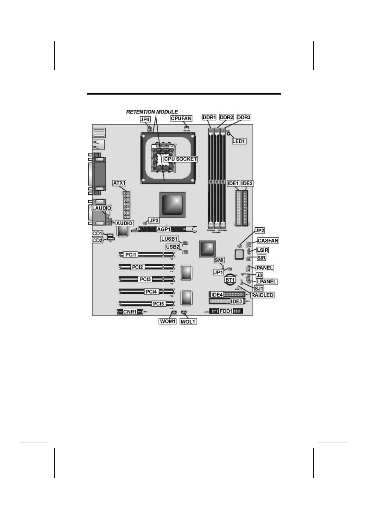
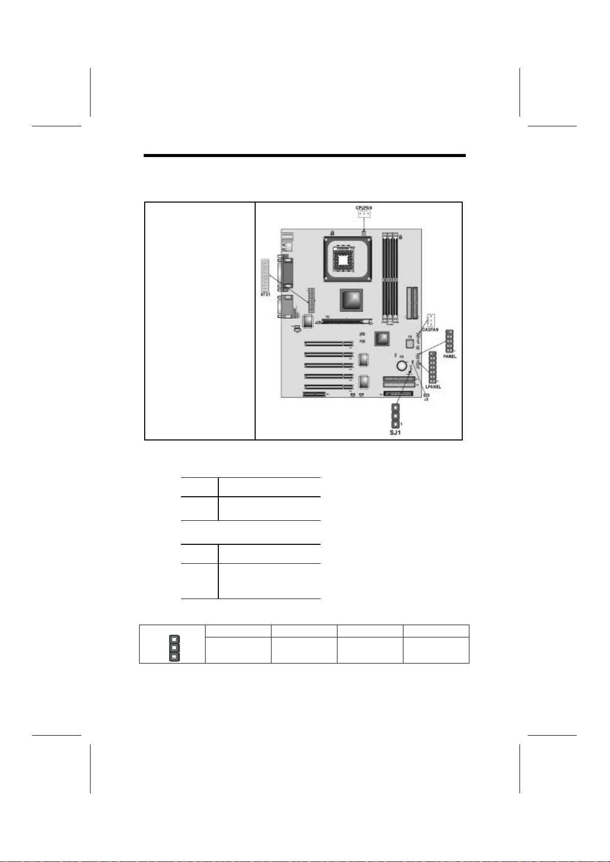
Table of Mainboard Components
Label Component
AGP1 Accelerated Graphics Port
ATX1 Power connector
AUDIO Mic/speaker-out connector
BT1 Three volt realtime clock battery
CASFAN Auxiliary case cooling fan
CD1 Primary CD-in connector (Sony)
CD2 Secondary CD-in connector (Panasonic)
CNR1 Communications Networking Riser slot
CPU SOCKET CPU Socket (mPGA478)
CPUFAN Cooling fan for CPU
DDRDIMM1 ~ DDRDIMM3 Three 184-pin DDR DIMM sockets
FDD1 Floppy disk drive connector
IDE 1 Primary IDE channel
IDE 2 Secondary IDE channel
IDE3 Third IDE channel for ATA 66/100
IDE4 Fourth IDE channel for ATA 66/100
J3 Single-color LED header
JP1 Clear CMOS jumper
JP2 BIOS protect jumper
JP3 CPU frequency select jumper
JP4 CPU voltage adjustment jumper
LAUDIO Mic/speaker-out connector 2
LED1 LED 2.5 VSB for DDR SDRAM (red)
LPANEL Front Panel Connector 2
LSIR Serial infrared cable header 2
LUSB1 Connector for front panel USB ports
PANEL Panel connector for case switches and LEDs
PCI1 ~ PCI5 Five 32-bit add-on card slots
RAIDLED IDE3/IDE4 array controller activeLED
SIR Serial infrared cable header
SJ1 Single-color LED header
SMI External System Management Interrupt header
USB2 Connector for front panel USB ports
WOL1 Wake On LAN wakeup connector
WOM1 Wake On Modem wakeup connector
Note: LED1 is usually connected to a light that indicates that the computer is
powered on. Do not install hardware or disconnect power cables while the
LED is on.
This concludes Chapter 1. The next chapter explains how to install the main-
board.

7
C
Ch
ha
ap
pt
te
er
r
2
2
Installing the Mainboard
S
Sa
af
fe
et
ty
y
P
Pr
re
ec
ca
au
ut
ti
io
on
ns
s
Follow these safety precautions when installing the mainboard:
•Wear a grounding strap attached to a grounded device to avoid
damage from static electricity.
•Discharge static electricity by touching the metal case of a safely
grounded object before working on the mainboard.
•Leave components in the static-proof bags they came in.
•Hold all circuit boards by the edges. Do not bend circuit boards.
Q
Qu
ui
ic
ck
k
G
Gu
ui
id
de
e
This Quick Guide suggests the steps you can take to assemble your system
with the mainboards.
The following table provides a reference for installing specific components:
Locating Mainboard Components Go to page 5
Installing the Mainboard in a Case Go to page 8
Setting Jumpers Go to page 8
Installing Case Components Go to page 11
Installing the CPU Go to page 13
Installing Memory Go to page 16
Installing a HDD and CD-ROM Drive Go to page 17
Installing a FDD Go to page 19
Installing Add-on Cards Go to page 19
Connecting Options Go to page 21
Connecting Peripheral (I/O) Devices Go to page 26
8
I
In
ns
st
ta
al
ll
li
in
ng
g
t
th
he
e
M
Ma
ai
in
nb
bo
oa
ar
rd
d
i
in
n
a
a
C
Ca
as
se
e
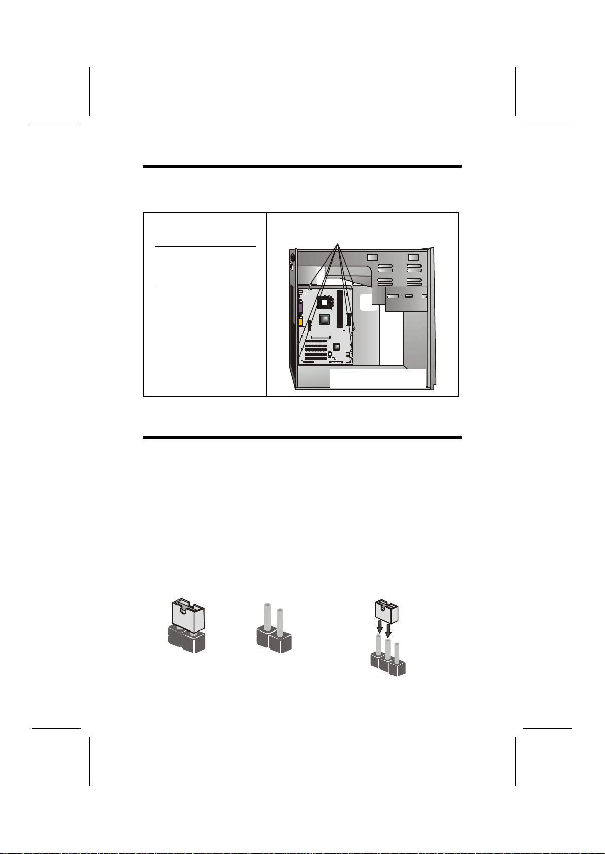
Refer to the following illustration and instructions for installing the mainboard
in a case:
This illustration shows an ex-
ample of a mainboard being
installed in a tower-type case:
Note: Do not overtighten
the screws as this
can stress the main-
board.
Most system cases have
mounting brackets installed in
the case, which correspond to
the holes in the mainboard.
Place the mainboard over the
mounting brackets and secure
the mainboard onto the mount-
ing brackets with screws.
2. Secure the mainboard with
screwswhereappropriate.
1. Place the mainboard
over the mounting brackets.
Ensure that your case has an I/O template that supports the I/O ports and
expansion slots on your mainboard.
C
Ch
he
ec
ck
ki
in
ng
g
J
Ju
um
mp
pe
er
r
S
Se
et
tt
ti
in
ng
gs
s
This section explains how to set jumpers for correct configuration of the main-
board.
Setting Jumpers
Use the mainboard jumpers to set system configuration options. Jumpers with
more than one pin are numbered. When setting the jumpers, ensure that the
jumper caps are placed on the correct pins.
The illustrations below show a 2-pin jumper.
When the jumper cap is placed on both pins,
the jumper is SHORT. If you remove the
jumper cap, or place the jumper cap on just
one pin, the jumper is OPEN.
This illustration shows a 3-pin
jumper. Pins 1 and 2 are SHORT.
ShortOpen 123

9
Checking Jumper Settings
The following illustration shows the location of the mainboard jumpers. Pin 1 is
labeled.
Jumper Settings
Jumper Type Description Setting (default)
JP1 3 pin Clear CMOS
jumper 1-2: Normal
2-3: Clear CMOS JP1
1
JP2 3 pin BIOS flash pro-
tection jumper 1-2: Unprotected
2-3: Protected
JP2
1
JP3 3 pin CPU Frequency
select jumper 1-2: Auto
2-3: 133 MHz JP3
1
JP4 9-pin CPU voltage
adjustment
jumper
1-2, 4-5, 7-8: Default
setting
See table on following
page for settings.
JP4
1
JP1 -This jumper enables you to reset BIOS. Follow these instructions:
1. Turn the system off.
2. Short pins 2 and 3 on JP1.
3. Return the jumper to the normal setting.
10
4. Turn the system on. The BIOS is returned to the de-
fault settings.
JP2 -This jumper is use to protect the BIOS from being unintentionally flashed.
JP3 -This jumper enables to set the CPU frequency.
JP4 -The CPU voltage is defined according to the VID table. VID4 and VID 3
are derived from the CPU only and cannot be changed. While VID0 ~ VID2
can be changed manually by setting the jumper 4 to adjust the CPU voltage.
However, this is not recommended. If you want to overclock, you might need
to increase the CPUvoltage.
•Auto –Set the CPU voltage according to its default setting.
Short pin numbers 1-2, 4-5, 7-8.
•Manual –Set the CPU voltage manually. Open all pins of jumper
4 and set the pin as follow: Where VID0 ~ VID2 are pin num-
bers 2-3, 5-6, 8-9 respectivelyof jumper 4. Thus, VID0 ~ VID2
will be equal to “0” by shorting pin numbers 2-3, 5-6, 8-9.
VID4 and VID3 depend on the CPU.
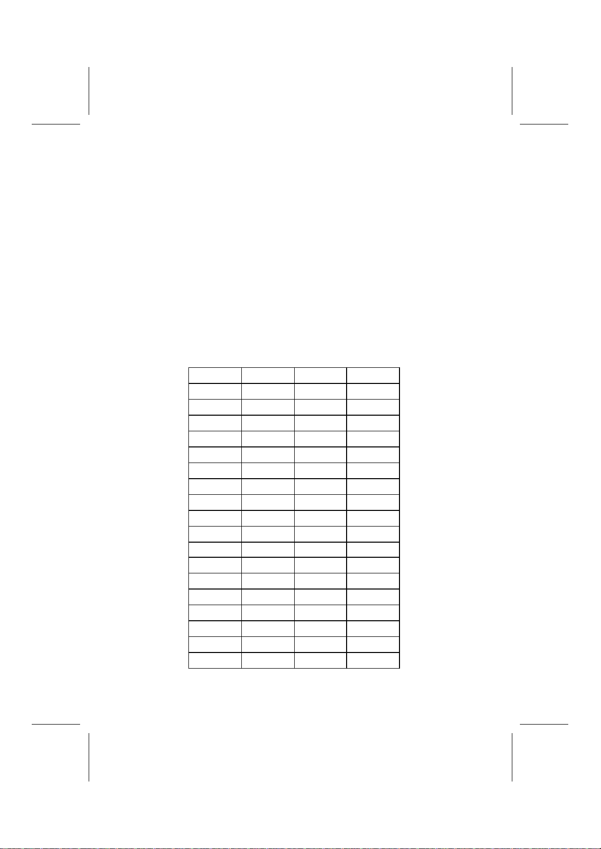
VID [4:0] Vcore (V) VID [4:0] Vcore (V)
00000 1.850 10000 1.450
00001 1.825 10001 1.425
00010 1.800 10010 1.400
00011 1.775 10011 1.375
00100 1.750 10100 1.350
00101 1.725 10101 1.325
00110 1.700 10110 1.300
00111 1.675 10111 1.275
01000 1.650 11000 1.250
01001 1.625 11001 1.225
01010 1.600 11010 1.200
01001 1.625 11001 1.225
01010 1.600 11010 1.200
01011 1.575 11011 1.175
01100 1.550 11100 1.150
01101 1.525 11101 1.125
01110 1.500 11110 1.100
01111 1.475 11111 No CPU
11
C
Co
on
nn
ne
ec
ct
ti
in
ng
g
C
Ca
as
se
e
C
Co
om
mp
po
on
ne
en
nt
ts
s
After you have installed the mainboard into a case, you can begin connecting
the mainboard components. Refer to the following:
1. Connect the case
power supply
connector to ATX1.
2. Connect the CPU
cooling fan cable to
CPUFAN.
3. Connect the case
cooling fan connector
to CASFAN.
4. Connect the case
LED cable to J3 or
SJ1.
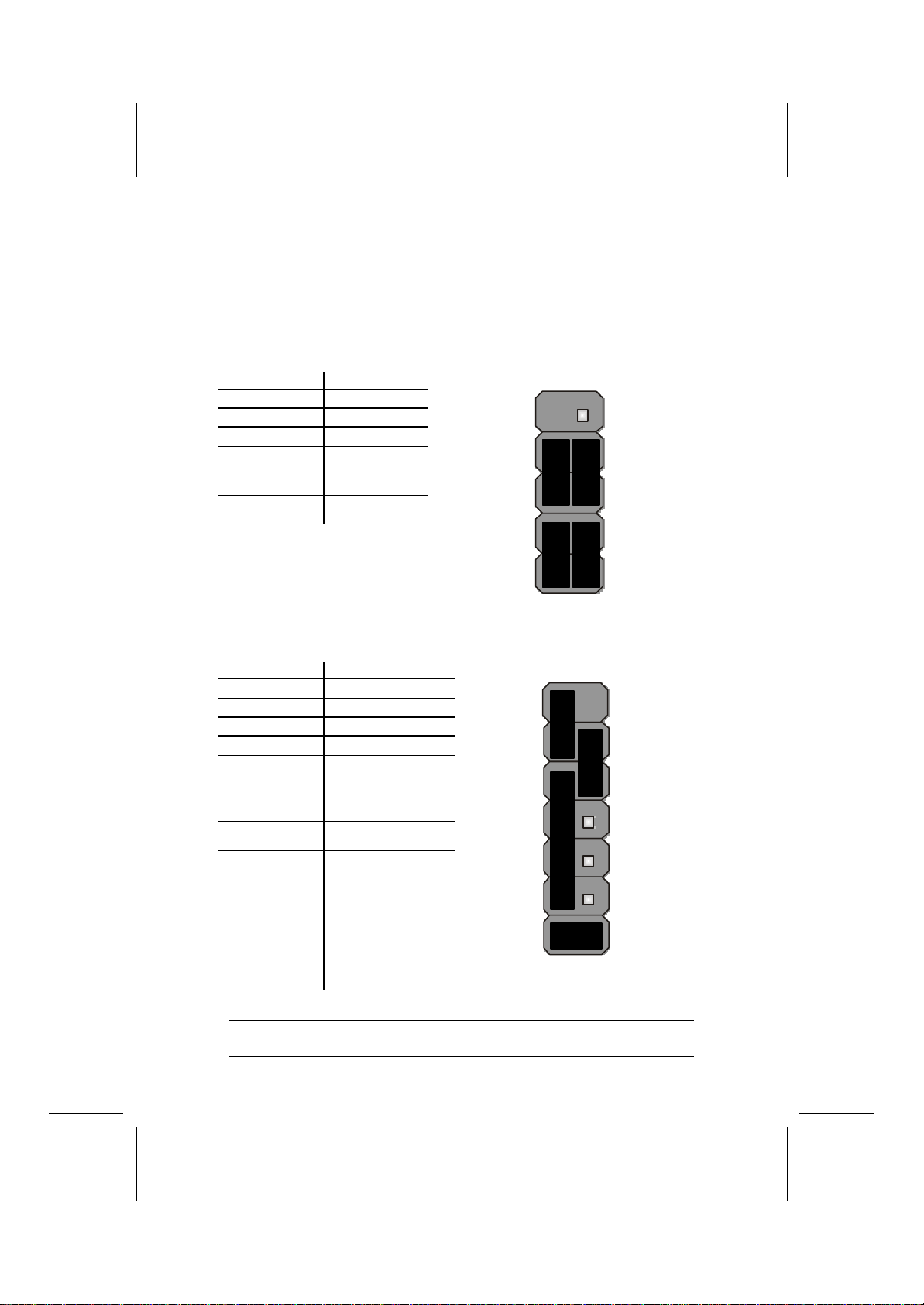
J3: Single color LED
Pin Signal Name
1
2LED +
Ground
SJ1: Single color LED header
Pin Signal Name
1
2
3
SUSLED-G
SUSLED-G
Ground
ACPI LED function:
S0 S1 S3 S4/S5
SJ1
1
Light Blinking Blinking Dark
12
The Panel Connectors
The panel connector (PANEL and LPANEL) provides a standard set of switch
and LED connectors commonly found on ATX or micro-ATX cases. The
LPANEL is specially designed for OEM customers that comply with the OEM
specifications. Refer to the table below for information:
PANEL
Device Pins
Empty 10
N/C 9
Power ON/OFF 6, 8
Reset Switch 5, 7
Green LED
Indicator 2, 4
HDD LED +1, -3
HDD LED
(Pins 1, 3)
2 1
Reset Switch
(Pins 5, 7)
Power Switch
(Pins 6, 8)
Green LED
(Pins 2, 4)
Empty
(Pin 10)
10 9
N/C
(Pin 9)
LPANEL
Device Pins
Reset Switch 12, 14
Case Speaker 4, 6, 8, 10
Power Switch 9, 11
Power LED +7
Green Power
LED -5
Yellow Power
LED -3
HDD LED +1, -2
HDD LED
(Pins 1, 2)
2 1
Reset Switch
(Pins 12, 14)
Case Speaker
(Pins 4, 6, 8, 10)
Yellow Power LED
(Pin 3)
Empty
(Pin 13)
14 13
Power Switch
(Pin 9, 11)
Green Power LED
(Pin 5)
Power LED
(Pin 7)
Note:The plus sign (+) indicates a pin which must be connected to a positive
voltage.

13
I
In
ns
st
ta
al
ll
li
in
ng
g
H
Ha
ar
rd
dw
wa
ar
re
e
Installing the Processor
Caution: When installing a CPU heatsink and cooling fan make sure that
you DO NOT scratch the mainboard or any of the surface-mount resistors
with the clip of the cooling fan. If the clip of the cooling fan scrapes
across the mainboard, you may cause serious damage to the mainboard
or its components.
On most mainboards, there are small surface-mount resistors near the
processor socket, which may be damaged if the cooling fan is carelessly
installed.
Avoid using cooling fans with sharp edges on the fan casing and the
clips. Also, install the cooling fan in a well-lit work area so that you can
clearly see the mainboard and processor socket.
Before installing the Processor
This mainboard automatically determines the CPU clock frequency and sys-
tem bus frequency for the processor. You may be able to change these
settings by making changes to jumpers on the mainboard, or changing the
settings in the system Setup Utility. We strongly recommend that you do not
overclock processors or other components to run faster than their rated speed.
Warning: Overclocking components can adversely affect the reliabilityof
the system and introduce errors into your system. Overclocking can per-
manently damage the mainboard by generating excess heat in
components that are run beyond the rated limits.
This mainboard has a Socket 478 processor socket. When choosing a proc-
essor, consider the performance requirements of the system. Performance is
based on the processor design, the clock speed and system bus frequency of
the processor, and the quantity of internal cache memory and external cache
memory.

14
CPU Installation Procedure
The following illustration shows CPU installation components:
Note: The pin-1 corner is marked with an arrow
Follow these instructions to install the CPU:
1. Install and secure the Retention Module on the mainboard.
2. Pull the CPU socket locking
lever away from the socket
to unhook it and raise the
locking lever to the upright
position.
3. Match the corner on the CPU marked with an arrow with pin-1 on the CPU
socket (the corner with the pinhole noticeably missing). Insert the processor
into the socket. Do not use force.
4. Lower the heatsink over the CPU.
5. Lower the CPU cooling fan onto the heatsink.
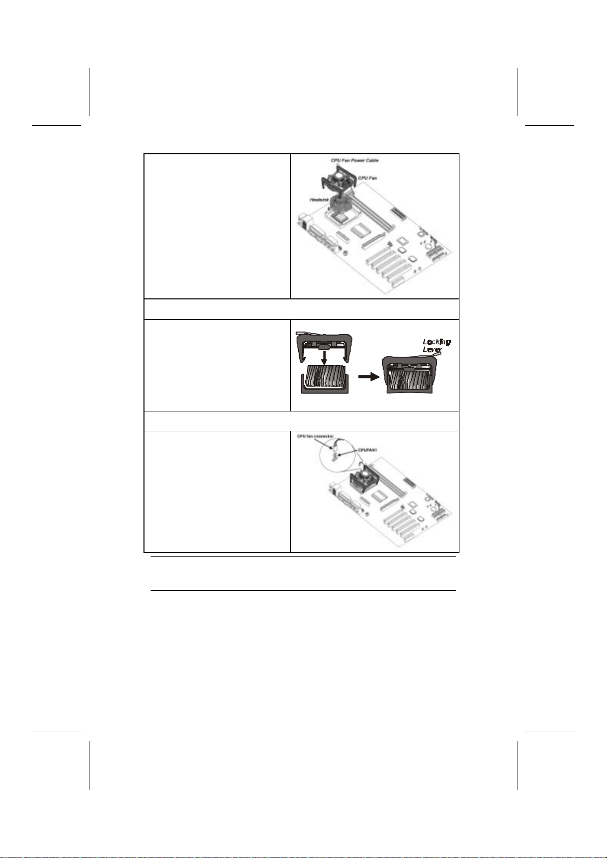
15
6. Apply thermal grease to the top
of the CPU.
7. Swing the locking lever down and hook it under the latch on the edge of the
socket.
8. Snap the four retention legs of
the cooling fan into place Cooling Fan
Retention Module
Heatsink
9. Swing both lock levers on top of the cooling fan to their opposite sides to se-
cure the cooling fan on top of the heatsink.
10. Connect the CPU Cooling Fan
power cable to the CPUFAN1
connector.
Note:CPU fan and heatsink installation procedures may vary with the type of
CPU fan/heatsink supplied. The form and size of fan/heatsink may also
vary.

16
Installing Memory Modules
This mainboard accommodates 184-pin 2.5V unbuffered Double Data Rate
(DDR) SDRAM memory modules. The memory chips must be standard or
registered SDRAM (Synchronous Dynamic Random Access Memory).
The memory bus can run at 100 MHz or 133 MHz. If your processor operates
over a 100 MHz system bus, you can install DDR200 or DDR266 memory
modules that operate over a 100 MHz or 133 MHz memory bus.
Installation Procedure
The mainboard accommodates three
memory modules. You must install at
least one module in any of the three
slots. Each module can be installed
with up to 1 GB of memory; total
memory capacity is 3 GB.
Refer to the following to install the memory modules.
1. Push the latches on each side of the DIMM slot down.
2. Align the memory module with the slot. The DIMM slots are keyed with
notches and the DIMMs are keyed with cutouts so that they can only be
installed correctly.
3. Check that the cutouts on the
DIMM module edge connector
match the notches in the
DIMM slot:
4. Install the DIMM module into
the slot and press it firmly
down until it seatscorrectly.
The slot latches are levered
upwards and latch on to the
edges of the DIMM.
5. Install any remaining DIMM
modules.
Cutout
Notch
Latch
Latch
Table of contents
Other ECS Electronics Motherboard manuals

ECS Electronics
ECS Electronics P6ISA-II User manual

ECS Electronics
ECS Electronics L7VMM User manual

ECS Electronics
ECS Electronics L4VXA User manual

ECS Electronics
ECS Electronics 648FX-A User manual

ECS Electronics
ECS Electronics L4IBAE User manual

ECS Electronics
ECS Electronics L7VTM User manual
 User manual")
ECS Electronics
ECS Electronics 661FX-M REV:1.0(B) User manual

ECS Electronics
ECS Electronics P6IEAT User manual

ECS Electronics
ECS Electronics L7VMM3 1.0 User manual

ECS Electronics
ECS Electronics M847 Series User manual


